
Mask at frequency domain and method for preparing the same and exposing system using the same
a frequency domain and mask technology, applied in the field of mask at frequency domain and a mask preparation method and an exposing system using the same, can solve the problems of interfering with the circuit layout of the wafer, and achieve the effect of simplifying the architecture, and optimizing the depth of focus
Patent Information
- Authority / Receiving Office
- US · United States
- Patent Type
- Patents(United States)
- Current Assignee / Owner
- Publication Date
- 2009-06-02
Smart Images
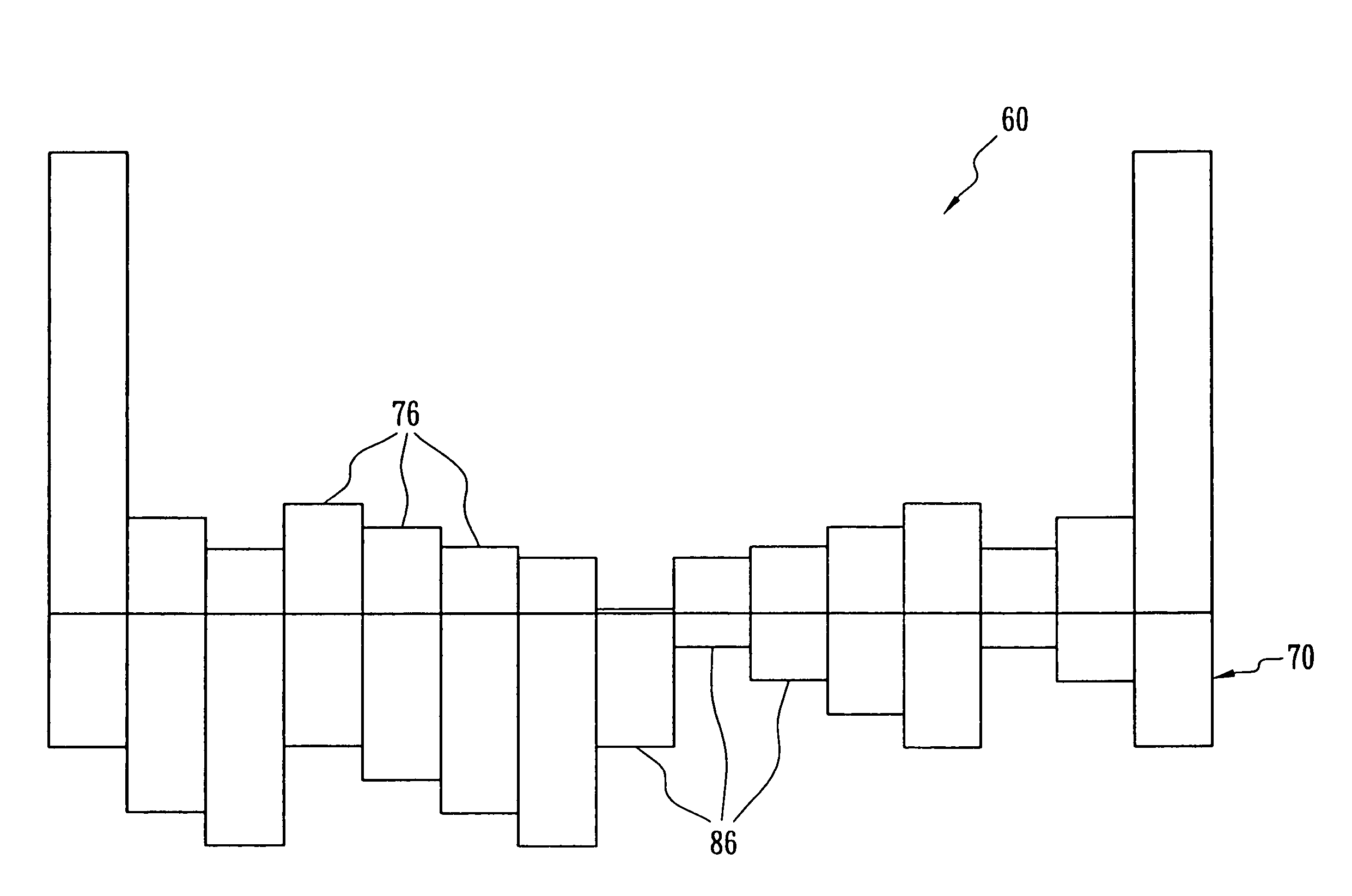
Figure 1 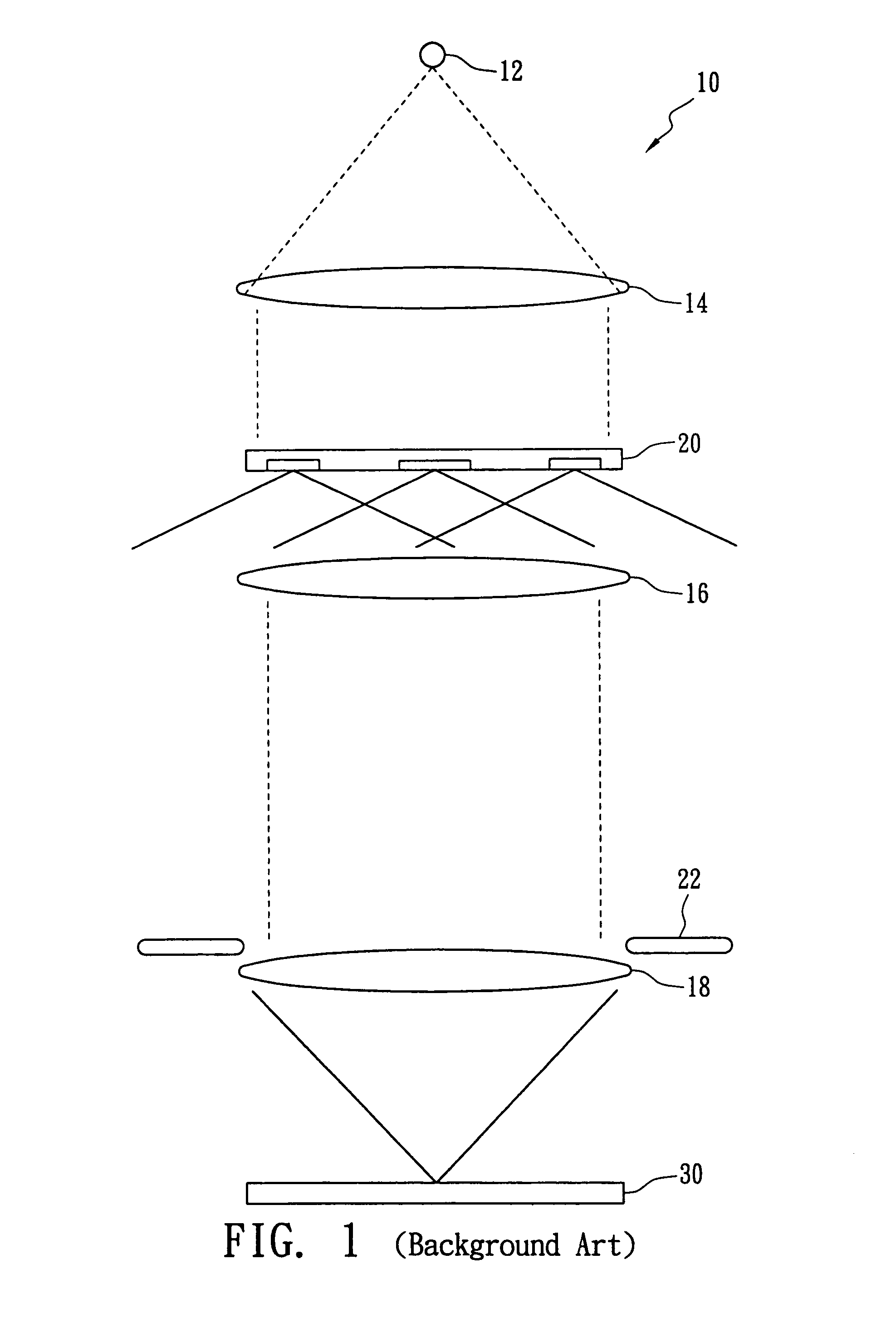
Figure 2 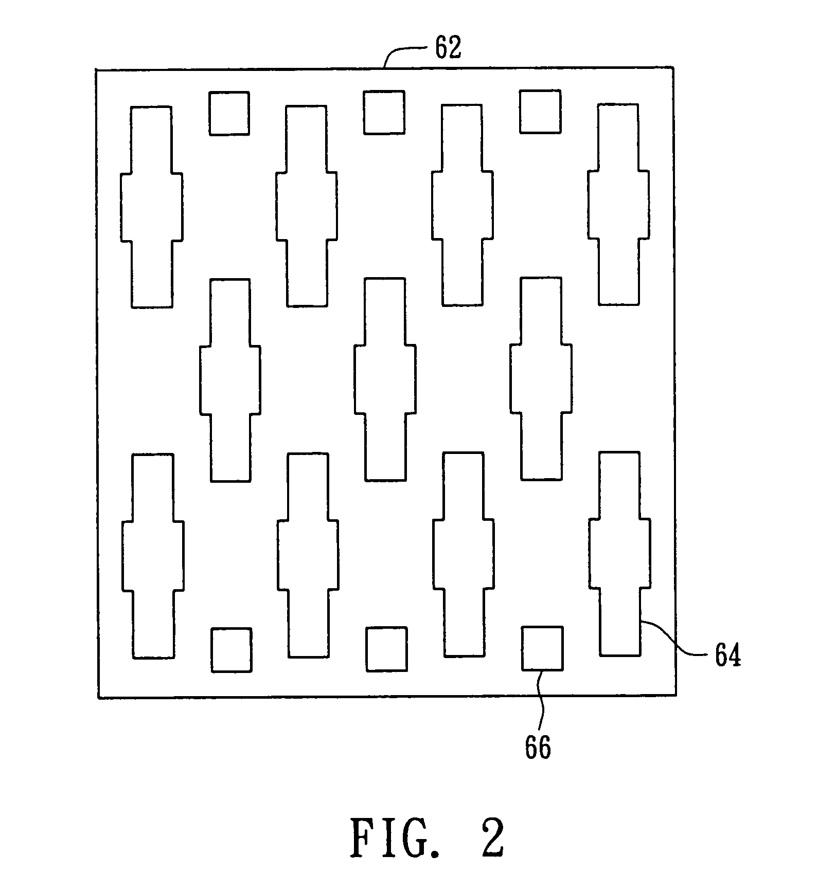
Figure 3
Abstract
Description
BACKGROUND OF THE INVENTION
[0001] (A) Field of the Invention
[0002] The present invention relates to a mask at frequency domain and a method for preparing the same and an exposing system using the same, and more particularly, to a mask at frequency domain, which has a plurality of amplitude patterns and a plurality of phase patterns generated from a circuit layout by Fourier transform process, and a method for preparing the same and an exposing system using the same.
[0003] (B) Description of the Related Art
[0004] FIG. 1 and FIG. 2 illustrate an exposing system 10 according to the prior art. From top to bottom, the exposing system 10 comprises an off-axis illumination (OAI) light source 12, a first lens 14, a mask 20, a second lens 16, a shielding plate 22, a third lens 18, and a wafer 30. The mask 20 includes a circuit layout 62 having two patterns 64 and 66, which are similar to the patterns to be formed on the wafer 30. Particularly, the difference between the patterns to be formed on ...
Examples
Embodiment Construction
[0015]FIG. 3 to FIG. 6 illustrate a method for preparing a mask 60 at frequency domain according to one embodiment of the present invention. First, a coordinate system such as the Cartesian coordinate system is overlaid onto a circuit layout 62 having a plurality of patterns 64 and 66, and the transparency of the circuit layout 62 on coordinate points of the coordinate system is calculated. The transparency is “1” if the coordinate point is inside the patterns 64 and 66, while the transparency is “0” if the coordinate point is outside the patterns 64 and 66. Subsequently, a Fast Fourier Transform (FFT) process is performed to generate an amplitude layout 72 and a phase layout 82 from the transparency distribution of the circuit layout 62, as shown in FIG. 4(a) and FIG. 4(b), respectively.
[0016]The amplitude layout 72 includes a plurality of first regions 74 having an amplitude value and the phase layout 82 includes a plurality of second regions 84 having a phase value. Preferably, t...