
Analog to digital converter having a non-linear ramp voltage
Patent Information
- Authority / Receiving Office
- US · United States
- Current Assignee / Owner
- Publication Date
- 2009-11-03
- Estimated Expiration
- Not applicable · inactive patent
Smart Images
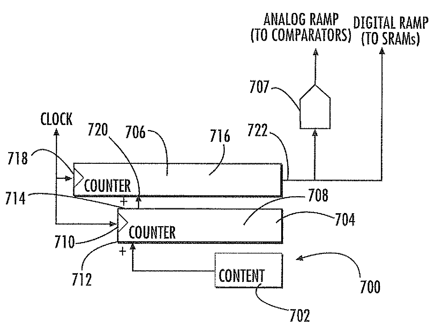
Figure 1 
Figure 2 
Figure 3
Abstract
Description
FIELD OF THE INVENTION
[0001] The invention relates to an analog to digital converter (ADC) having a non-linear ramp voltage for use in an image sensor. More particularly, but not exclusively, the invention relates to an ADC having a smooth non-linear ramp voltage for use in a complementary metal oxide semiconductor (CMOS) based image sensor.BACKGROUND OF THE INVENTION
[0002] There are two types of commonly used image sensors, Charge Coupled Devices (CCDs) and (CMOS) sensors. Both CCD and CMOS image sensors convert photons into electrons via the interaction of photons with a semiconductor, typically silicon.
[0003] CCD sensors transfer charge within the silicon using electric fields and require high charge transfer efficiency (CTE), close to 100%. Consequently, the manufacturing of CCD sensor is tailored to maximize or increase the CTE associated with the device. This involves dopant implantations that result in the substrate being unsuitable for high performance transistor manufacture.[0...
Examples
Embodiment Construction
[0044]Referring now to FIG. 7, a non-linear, typically quadratic digital ramp generator 700 comprises a memory device 702, an incremental counter 704, a ramp counter 706, and a DAC 707. In a preferred embodiment, the counters 704, 706 are shift registers. The incremental counter 704 comprises a processor 708, a clock input 710, an additive input 712 and an output 714.
[0045]The ramp counter 706 comprises a processor 716, a clock input 718, an incremental input 720 and an output 722. The incremental counter 704 and the ramp counter 706 receive a clock signal from the same clock (not shown) at their respective clock inputs 710, 718. Receipt of the clock signal triggers the processor 716 of the ramp counter 706 to output a ramp code RAMP, currently stored at the ramp counter 706, to a DAC and a data storage device via the output 722.
[0046]Typically, the ramp counter will have an initial code of zero, although non-zero initial codes are possible. Receipt of the clock signal triggers the ...