
Pre-aligned metrology system and modules
a metrology system and module technology, applied in the field of optical metrology, can solve the problems of further complications, challenge for sem to meet the metrology request, etc., and achieve the effect of improving the reliability and availability of the ims
Patent Information
- Authority / Receiving Office
- US · United States
- Patent Type
- Patents(United States)
- Current Assignee / Owner
- Publication Date
- 2011-05-10
- Estimated Expiration
- Not applicable · inactive patent
Smart Images
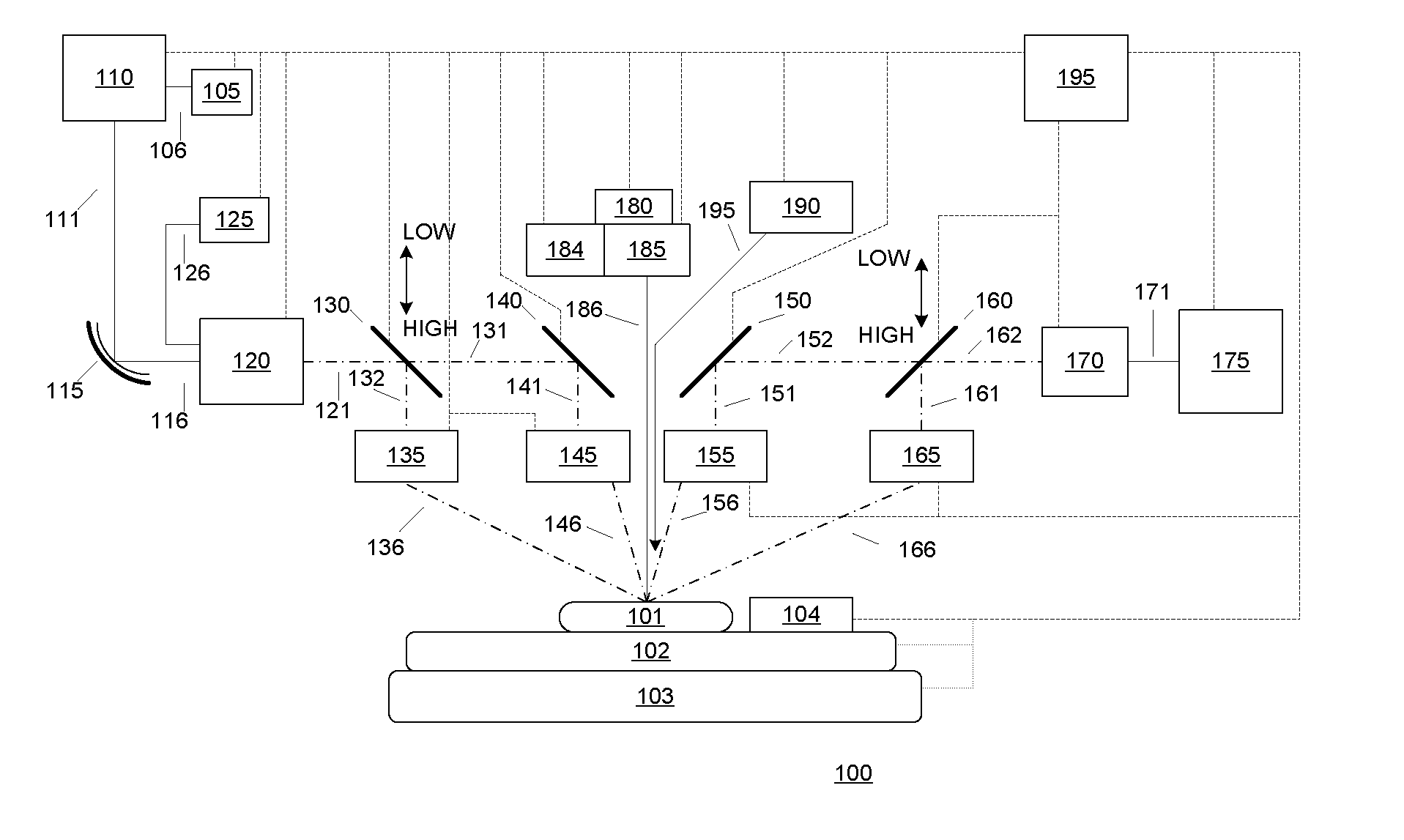
Figure 1 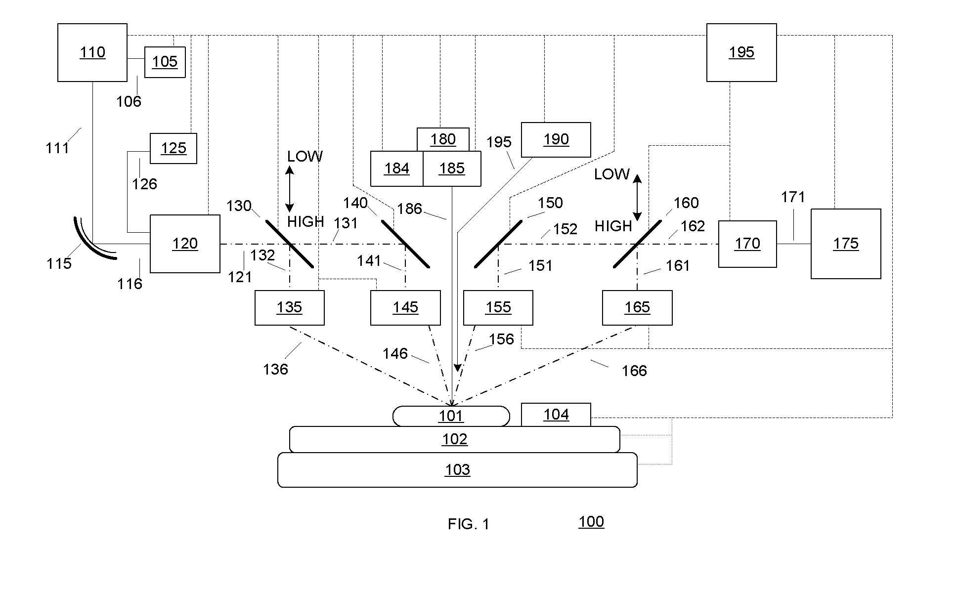
Figure 2 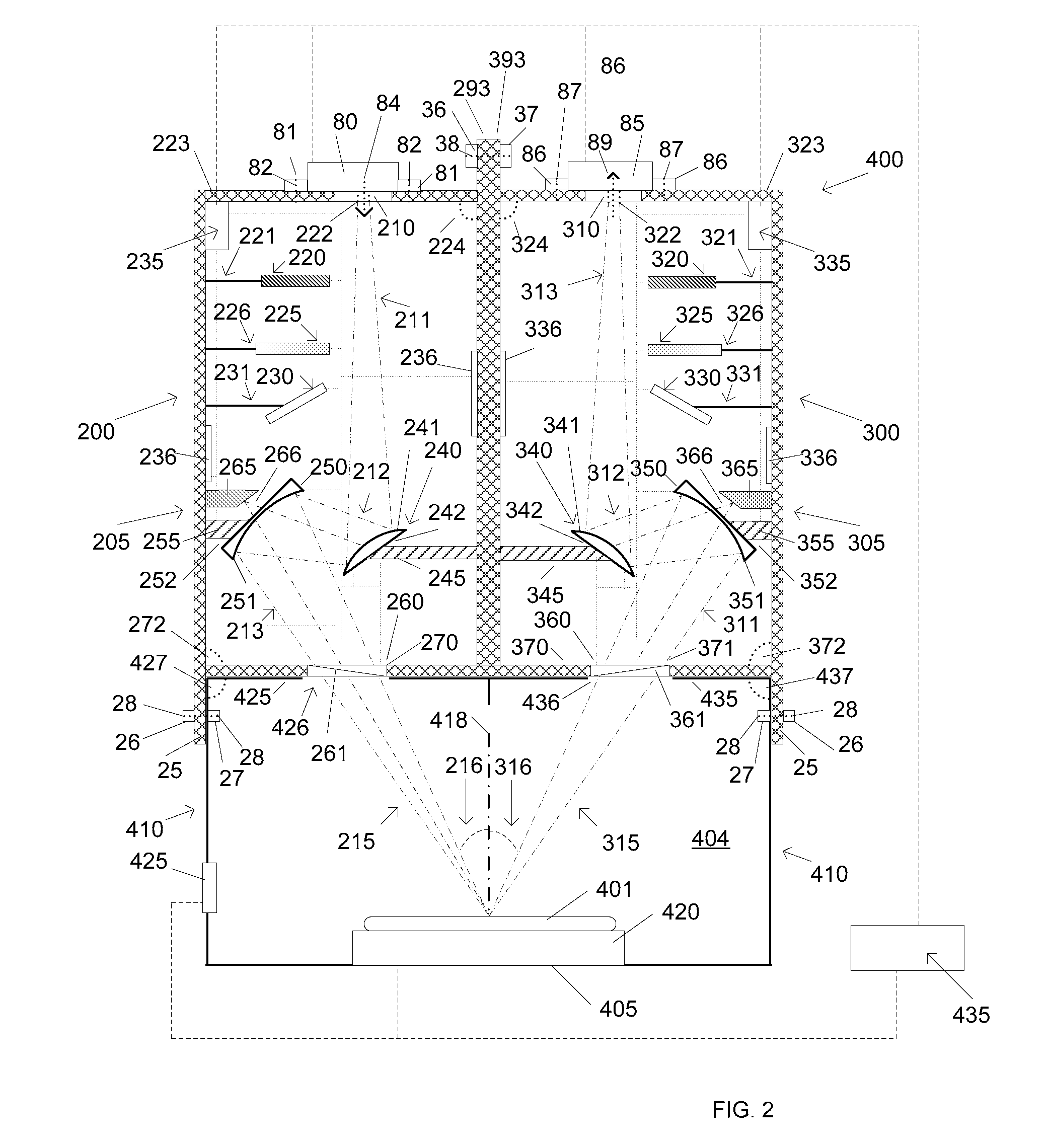
Figure 3
Abstract
Description
BACKGROUND OF THE INVENTION
[0001] 1. Field of the Invention
[0002] The present invention relates to optical metrology, and more particularly to improving the optical metrology process using a pre-aligned metrology system that includes pre-aligned metrology assemblies and pre-aligned metrology modules.
[0003] 2. Description of the Related Art
[0004] In the manufacture of integrated circuits, very thin lines or holes down to 10 nm or sometimes smaller are patterned into photoresist and then transferred using an etching process into a layer of material below on a silicon wafer. It is extremely important to inspect and control the width and profile (also known as critical dimensions or CDs) of these lines or holes. Traditionally the inspection of CDs that are smaller than the wavelength of visible light has been done using large and expensive scanning electron microscopes (SEM). As the structures patterned get smaller and smaller, the measurement precision and accuracy becomes much higher, and...
Examples
Embodiment Construction
[0015]Reliability, availability, and performance are the most important parameters for semiconductor equipments in a modern fabrication environment. Many semiconductor manufacturers use optical metrology systems for thin-film and optical CD measurements that include stand-alone tools, and use off-line applications for process monitoring. As the semiconductor roadmap goes to smaller and smaller nodes, the tightened tolerances associated with the smaller structures become more challenging to obtain and verify using semiconductor process control applications. Thus, integrated metrology tools are required to meeting measurement time and accuracy on the smaller structures made on the wafer. In addition, the measured data from the integrated metrology sensor (IMS) can be used either to optimize the process tools that are being used to create the structures on the wafer, or to adjust the process tool conditions that are being used to further process the wafer. When the metrology tool is in...