
Defect review apparatus and method for correcting coordinate misalignment using two light sources
a technology of coordinate misalignment and defect detection, applied in the field of defect detection techniques, can solve the problems of hardly likely capture of defects, inaccurate defect coordinate acquired from inspection apparatus, and decrease in yield rate, so as to improve the throughput and reliability of sem observation
Patent Information
- Authority / Receiving Office
- US · United States
- Patent Type
- Patents(United States)
- Current Assignee / Owner
- Publication Date
- 2017-09-19
Smart Images
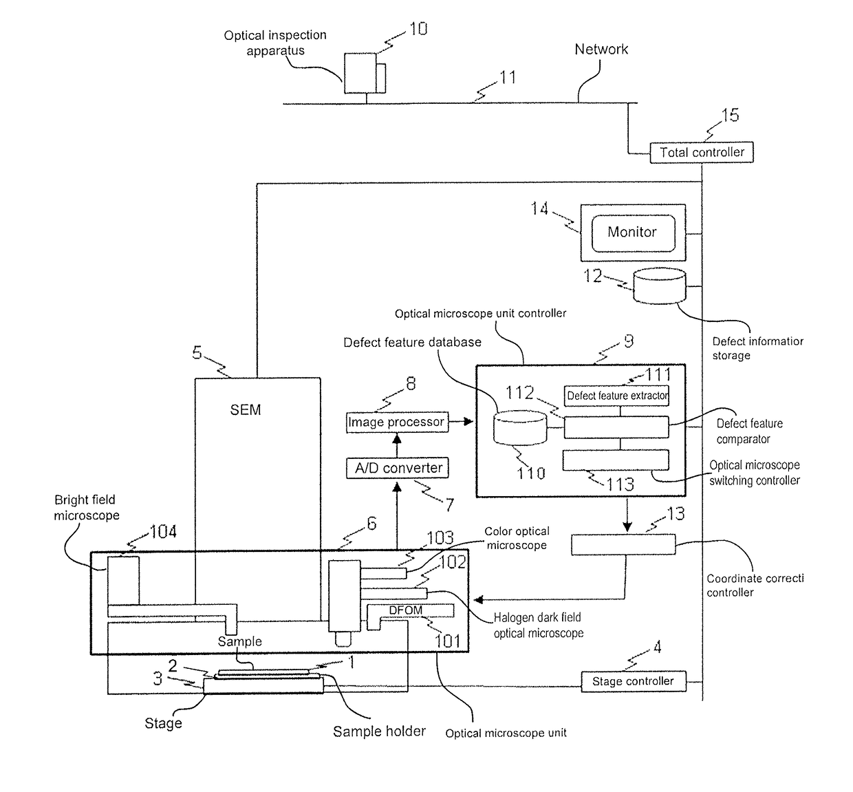
Figure 1 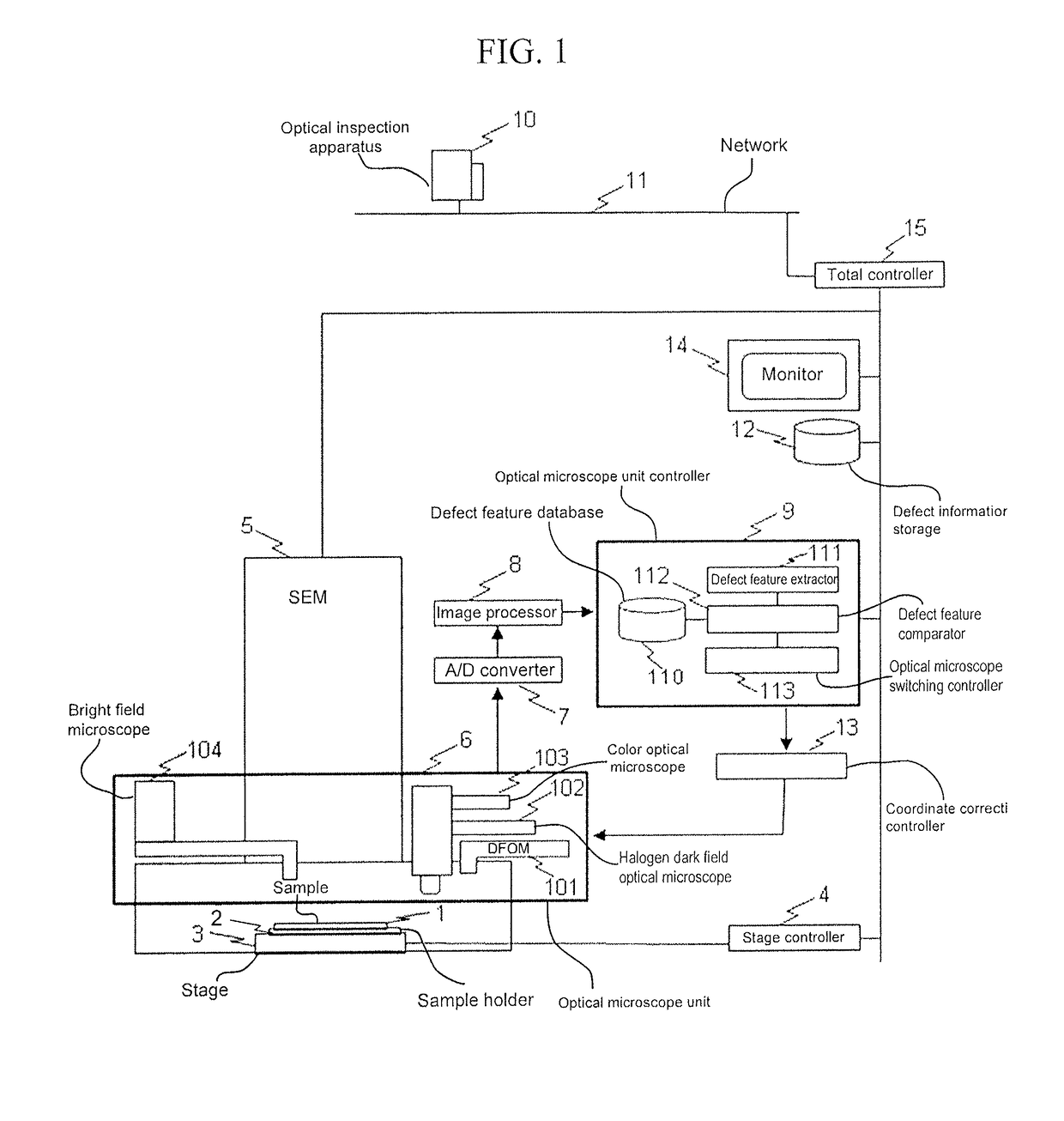
Figure 2 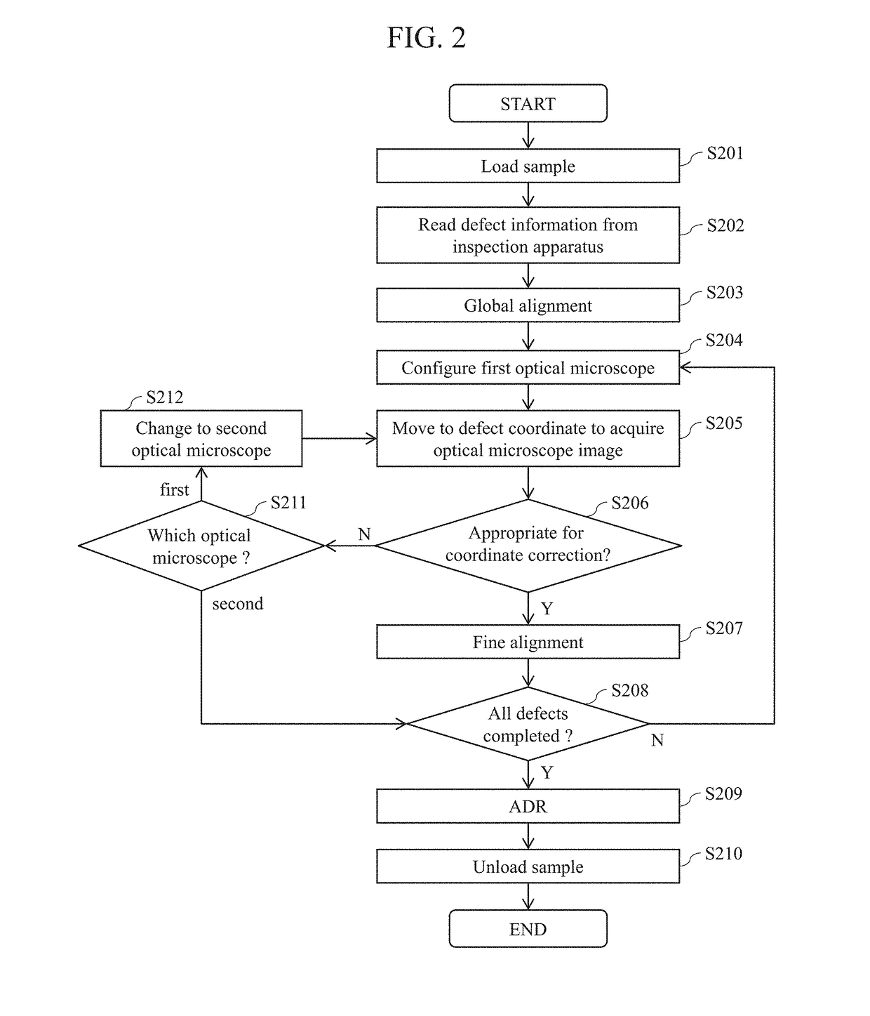
Figure 3
Abstract
Description
CLAIM OF PRIORITY
[0001] The present application claims priority from Japanese patent application JP 2014-079544 filed on Apr. 8, 2014, the content of which is hereby incorporated by reference into this application.BACKGROUND
[0002] Technical Field
[0003] The present invention relates to a defect review techniques for observing defects on samples detected by inspection devices to acquire detailed information of the observed defects.
[0004] Background Art
[0005] In manufacturing processes for such as semiconductor devices, processes such as film formation, lithographic exposure, or etching are repeated to form micro-circuit patterns on semiconductor samples via hundreds of processes (hereinafter, semiconductor samples are referred to as samples). In these manufacturing processes, decrease in yield rate may be caused by foreign particles generated on the sample due to errors or improper maintenances of process manufacturing devices or to mismatch in manufacturing conditions, or may be caused by...
Examples
embodiment 1
[0049]As discussed thus far, if it is impossible to observe the defect using the DFOM 101, the defect review apparatus according to the embodiment 1 checks the defect size on the basis of the defect information, and switches the DFOM 101 into the halogen bright field optical microscope 104 if the defect is a huge defect. Accordingly, even in cases where the inspection apparatus 10 observes huge defects which coordinate is difficult to be precisely acquired, the halogen bright field optical microscope 104 acquires precise coordinates and the coordinate correction controller 13 may correct the coordinate misalignment according to the precisely acquired coordinates.
[0050]It can be assumed that only the DFOM 101 may be used as another method for performing fine alignment with respect to huge defects and a search-around functionality may be used. In other words, the field of view is rotationally changed until the defect is found to search the defect, thereby acquiring the correct coordin...
embodiment 2
[0062]As discussed thus far, if it is impossible to observe the defect using the DFOM 101, the defect review apparatus according to the embodiment 2 compares the defect feature with the features stored in the defect feature DB 110 in advance. If those features match with each other, the DFOM 101 is switched into the halogen dark field optical microscope 102 or into the color optical microscope 103. Accordingly, even in cases where the inspection apparatus 10 observes tailing defects which coordinate may be positioned at wrong coordinate, the halogen dark field optical microscope 102 or the color optical microscope 103 may position the correct coordinate and the coordinate correction controller 13 may correct the coordinate misalignment according to the precisely positioned coordinates.
[0063]It can be assumed that the type of optical microscope may not be changed and only the image processing may be used to avoid positional misalignment as another method for performing fine alignment...