

Magnesium Yttrium Alloy Biomedical Modified Alloy: Advanced Compositions, Processing Strategies, And Clinical Applications
JUL 16, 20259 MIN READ
Generate Your Research Report Instantly with AI Agent
PatSnap Eureka helps you evaluate technical feasibility & market potential.
Chiplet Communication Evolution and Objectives
Chiplet communication has evolved significantly over the past decade, driven by the increasing demand for high-performance computing and the limitations of traditional monolithic chip designs. The evolution of chiplet communication protocols reflects the industry's shift towards modular and scalable chip architectures, enabling more efficient and cost-effective semiconductor manufacturing processes.
Initially, chiplet communication relied on simple point-to-point interfaces, which were limited in bandwidth and scalability. As the need for higher data transfer rates and more complex chip designs grew, the industry developed more sophisticated protocols. This led to the emergence of advanced interconnect technologies such as Intel's Embedded Multi-die Interconnect Bridge (EMIB) and AMD's Infinity Fabric.
The primary objectives of chiplet communication protocols are to facilitate seamless integration of multiple dies within a single package, maximize data transfer rates, minimize latency, and ensure power efficiency. These protocols aim to provide a standardized approach to inter-die communication, allowing for greater flexibility in chip design and manufacturing.
One of the key milestones in chiplet communication was the introduction of the Advanced Interface Bus (AIB) by Intel in 2017. AIB provided a standardized interface for chiplet-to-chiplet communication, enabling higher bandwidth and lower power consumption compared to previous solutions. This development paved the way for more widespread adoption of chiplet-based designs across the industry.
In recent years, the focus has shifted towards developing open standards for chiplet communication. The Universal Chiplet Interconnect Express (UCIe) consortium, formed in 2022, aims to create a unified standard for die-to-die interconnects. This initiative represents a significant step towards interoperability and ecosystem development in the chiplet space.
The evolution of chiplet communication protocols has also been influenced by advancements in packaging technologies. The development of 2.5D and 3D packaging solutions has enabled closer integration of chiplets, reducing communication distances and improving overall system performance. This has led to the need for protocols that can support ultra-short reach (USR) communication with extremely low latency and high bandwidth.
Looking ahead, the objectives for future chiplet communication protocols include achieving even higher data rates, further reducing power consumption, and supporting more complex multi-chiplet configurations. There is also a growing emphasis on developing protocols that can facilitate heterogeneous integration, allowing for the seamless combination of chiplets manufactured using different process nodes or by different vendors.
Market Demand Analysis for Chiplet Technology
The chiplet technology market is experiencing significant growth, driven by the increasing demand for high-performance computing solutions across various industries. As traditional monolithic chip designs reach their physical limits, chiplets offer a scalable and cost-effective alternative, enabling the integration of multiple specialized components on a single package. This approach allows for improved performance, reduced power consumption, and enhanced flexibility in chip design.
The market demand for chiplet technology is particularly strong in data centers, cloud computing, artificial intelligence, and edge computing applications. These sectors require increasingly powerful and efficient processors to handle complex workloads and massive data processing tasks. Chiplets provide a solution by allowing the combination of different process nodes and specialized functions, optimizing performance and cost.
In the consumer electronics market, chiplets are gaining traction in smartphones, tablets, and other mobile devices. The technology enables manufacturers to create more powerful and energy-efficient devices while maintaining compact form factors. This trend is expected to accelerate as 5G networks become more widespread, driving demand for advanced mobile processors.
The automotive industry is another key driver of chiplet technology adoption. As vehicles become more connected and autonomous, there is a growing need for sophisticated computing systems that can handle complex sensor data processing, real-time decision-making, and advanced driver assistance features. Chiplets offer a flexible and scalable solution to meet these evolving requirements.
The market for chiplet technology is also expanding in the industrial and healthcare sectors. In industrial applications, chiplets enable the development of more efficient and intelligent control systems for manufacturing processes and robotics. In healthcare, chiplets support the creation of advanced medical imaging equipment, wearable devices, and diagnostic tools that require high-performance computing capabilities in compact form factors.
As the demand for chiplet technology grows, the market is witnessing increased investment in research and development from major semiconductor companies and startups alike. This has led to rapid advancements in chiplet design, packaging, and integration techniques. The development of standardized interfaces and communication protocols for chiplets is further accelerating market adoption by enabling interoperability between different vendors' components.
The chiplet market is expected to see substantial growth in the coming years, with analysts projecting a compound annual growth rate (CAGR) in the double digits. This growth is driven by the technology's ability to address the increasing complexity and performance requirements of modern computing systems while offering improved cost-effectiveness and design flexibility compared to traditional monolithic chip architectures.
Current Challenges in Chiplet Interconnect
As chiplet technology continues to advance, several significant challenges have emerged in the realm of chiplet interconnect. One of the primary issues is the need for high-bandwidth, low-latency communication between chiplets. Traditional interconnect technologies struggle to meet the increasing demands of data transfer rates required for complex multi-chiplet systems. This challenge is further compounded by the need to maintain signal integrity over short distances while minimizing power consumption.
Another critical challenge lies in the standardization of chiplet interfaces. The lack of widely adopted industry standards for chiplet communication protocols hinders interoperability and limits the potential for mix-and-match chiplet designs from different vendors. This fragmentation in the ecosystem creates barriers to entry for smaller players and slows down overall innovation in the field.
Thermal management presents yet another hurdle in chiplet interconnect design. As chiplets are packed more densely and communicate at higher frequencies, heat dissipation becomes a significant concern. Effective thermal solutions must be developed to ensure reliable operation and prevent performance degradation due to thermal throttling.
The challenge of die-to-die alignment and bonding accuracy also cannot be overlooked. As the number of interconnects between chiplets increases, the precision required for aligning and bonding these components becomes more critical. Even slight misalignments can lead to connection failures or degraded performance, impacting the overall system reliability.
Power delivery and distribution across multiple chiplets pose another set of challenges. Ensuring consistent and adequate power supply to each chiplet while managing voltage drops and current fluctuations requires sophisticated power delivery network designs. This becomes increasingly complex as the number of chiplets in a system grows.
Testing and validation of chiplet-based systems present unique challenges compared to monolithic designs. Developing effective test methodologies for individual chiplets as well as the integrated system is crucial for ensuring quality and reliability. This includes addressing issues such as known-good-die testing and system-level debugging in multi-chiplet environments.
Lastly, the challenge of cost-effective packaging solutions for chiplet-based designs remains significant. Advanced packaging technologies that can accommodate high-density interconnects while maintaining manufacturability and yield are essential for the widespread adoption of chiplet architectures. Balancing performance requirements with cost considerations continues to be a key focus area for researchers and industry professionals in the chiplet ecosystem.
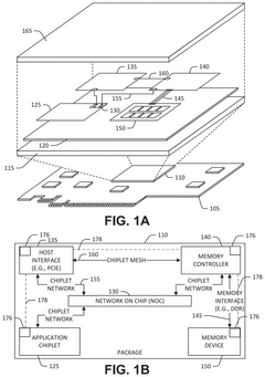
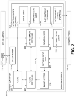
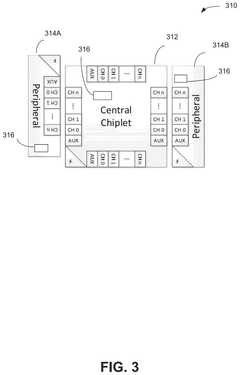
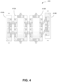
Existing Chiplet Communication Protocols
01 Inter-chiplet communication protocols
Various protocols are developed for efficient communication between chiplets in multi-chip systems. These protocols define standards for data transfer, addressing, and synchronization between different chiplets, enabling high-speed and low-latency communication within the system.- Inter-chiplet communication protocols: Various protocols are developed for efficient communication between chiplets in multi-chip systems. These protocols define standards for data transfer, addressing, and synchronization between different chiplets, enabling high-speed and low-latency communication within the system.
- Network-on-Chip (NoC) for chiplet interconnection: Network-on-Chip architectures are utilized to facilitate communication between chiplets. NoC provides a scalable and flexible interconnect solution, allowing for efficient data routing and reduced latency in complex multi-chiplet designs.
- Packaging technologies for chiplet integration: Advanced packaging technologies are developed to integrate multiple chiplets into a single package. These technologies focus on improving thermal management, signal integrity, and power delivery while enabling high-bandwidth communication between chiplets.
- Standardization of chiplet interfaces: Efforts are made to standardize chiplet interfaces and protocols to ensure interoperability between chiplets from different manufacturers. This standardization aims to create a more open and flexible ecosystem for chiplet-based designs.
- Power management in chiplet communication: Techniques are developed to optimize power consumption in chiplet communication. These include dynamic voltage and frequency scaling, power gating, and adaptive link management to improve energy efficiency in multi-chiplet systems.
02 Network-on-Chip (NoC) for chiplet interconnection
Network-on-Chip architectures are implemented to facilitate communication between chiplets. NoC provides a scalable and flexible interconnect solution, allowing for efficient data routing and reduced latency in multi-chiplet systems.Expand Specific Solutions03 Packaging technologies for chiplet integration
Advanced packaging technologies are developed to integrate multiple chiplets into a single package. These technologies focus on improving signal integrity, thermal management, and power delivery between chiplets, enhancing overall system performance.Expand Specific Solutions04 Standardization of chiplet interfaces
Efforts are made to standardize chiplet interfaces, allowing for interoperability between chiplets from different manufacturers. These standards define common protocols, electrical specifications, and physical interfaces to facilitate seamless integration of diverse chiplets.Expand Specific Solutions05 Power management and optimization in chiplet communication
Techniques are developed to optimize power consumption in chiplet communication. These include adaptive power gating, dynamic voltage and frequency scaling, and intelligent routing algorithms to minimize energy usage while maintaining high performance in multi-chiplet systems.Expand Specific Solutions
Key Players in Chiplet Ecosystem
The chiplet communication protocols market is in a growth phase, driven by increasing demand for high-performance computing and data-intensive applications. The market size is expanding rapidly, with major players like Intel, TSMC, and Micron Technology investing heavily in chiplet technology. The technical maturity varies, with some established protocols and others still in development. Companies like Huawei, Qualcomm, and AMD are actively researching and implementing chiplet designs, while newer entrants like Rebellions Inc. are focusing on AI-specific chiplet solutions. The competitive landscape is dynamic, with both semiconductor giants and specialized startups vying for market share in this emerging field.
Huawei Technologies Co., Ltd.
Technical Solution: Huawei has developed the Kirin System-in-Package (SiP) technology for chiplet integration in their mobile processors. This approach uses a combination of 2.5D and 3D packaging techniques to integrate multiple chiplets into a single package[7]. Huawei's chiplet communication protocol focuses on high-bandwidth, low-latency connections between the main SoC and auxiliary chiplets, such as AI accelerators or modems. The company has also been working on advanced packaging technologies like fan-out wafer-level packaging (FOWLP) to improve chiplet integration and communication[8]. These technologies enable data rates of up to 6 Gbps between chiplets while maintaining power efficiency.
Strengths: Optimized for mobile applications, high integration density, and improved power efficiency. Weaknesses: Potential geopolitical challenges and limited adoption outside of Huawei's ecosystem.
QUALCOMM, Inc.
Technical Solution: Qualcomm has developed the High-Speed Low-Power (HSLP) interface for chiplet communication. HSLP is designed to provide high-bandwidth, low-latency connections between chiplets while maintaining low power consumption. The protocol supports data rates up to 100 Gbps per link[5]. Qualcomm has also introduced their own implementation of the Universal Chiplet Interconnect Express (UCIe) standard, which aims to provide a unified interface for chiplet communication across different vendors[6]. UCIe supports both die-to-die and package-to-package interconnects, with data rates ranging from 16 GT/s to 32 GT/s in its first version.
Strengths: High-speed data transfer, low power consumption, and support for industry standards. Weaknesses: Potential interoperability challenges with other vendors' implementations.
Innovative Interconnect Technologies
Method for configuring multiple input-output channels
PatentPendingUS20250118343A1
Innovation
- The implementation of a chiplet protocol interface (CPI) network, which includes a packet-based network with virtual channels, enables flexible and high-speed interaction between chiplets. This network uses a credit-based flow control technique and includes elements to minimize latency and energy consumption in ultra-short reach chiplet interconnects.
Chiplet-to-chiplet protocol switch
PatentWO2025006403A1
Innovation
- A bonded structure comprising a carrier with a protocol switch die that converts communication signals from one protocol to another, directly bonded to chiplets without intervening adhesives, utilizing processing circuitry to detect and convert between various communication protocols based on factors like architecture, data rate, and voltage levels, ensuring seamless communication between chiplets.

Standardization Efforts in Chiplet Industry
The chiplet industry has recognized the critical need for standardization to ensure interoperability and foster innovation. Several key organizations and initiatives have emerged to address this challenge, driving the development of common protocols and interfaces for chiplet-based systems.
One of the most prominent efforts is the Universal Chiplet Interconnect Express (UCIe) consortium, formed in 2022. UCIe aims to establish an open industry standard for die-to-die interconnects, enabling seamless integration of chiplets from different vendors. The consortium includes major players such as Intel, AMD, Arm, TSMC, and Samsung, highlighting the industry-wide commitment to standardization.
Another significant initiative is the Open Compute Project (OCP), which has established the Open Domain-Specific Architecture (ODSA) workgroup. The ODSA focuses on developing open architectures and specifications for chiplet-based systems, including the Bunch of Wires (BoW) interface and the OpenHBI (Open High-Bandwidth Interface) specification.
The JEDEC Solid State Technology Association has also been active in chiplet standardization efforts. They have formed the JC70 Committee on Wide I/O Memories, which is working on standards for high-bandwidth memory interfaces that are crucial for chiplet-based designs.
In addition to these industry consortia, government-backed initiatives are also contributing to standardization efforts. For example, the DARPA CHIPS (Common Heterogeneous Integration and IP Reuse Strategies) program in the United States aims to develop modular chip designs and standardized interfaces for military and commercial applications.
The IEEE has also recognized the importance of chiplet standardization and has initiated the P3047 working group. This group is developing standards for 2.5D and 3D die-to-die interfaces, which are essential for chiplet integration.
These standardization efforts are crucial for the widespread adoption of chiplet technology. They aim to create a common language for chiplet communication, enabling designers to mix and match chiplets from different vendors and fabrication processes. This interoperability is expected to accelerate innovation, reduce costs, and improve time-to-market for complex semiconductor systems.
As these standards mature, we can expect to see increased collaboration between chipmakers, foundries, and system integrators. The development of standardized chiplet interfaces will likely lead to the emergence of a more diverse and competitive chiplet ecosystem, benefiting both manufacturers and end-users of advanced computing systems.
Performance Benchmarking of Protocols
Performance benchmarking is a critical aspect of evaluating chiplet communication protocols. It provides quantitative data on the efficiency, speed, and reliability of different protocols, enabling designers to make informed decisions when selecting the most suitable solution for their specific applications.
One of the primary metrics used in benchmarking chiplet communication protocols is bandwidth. This measure indicates the amount of data that can be transferred between chiplets in a given time frame. High-bandwidth protocols are essential for applications requiring rapid data exchange, such as high-performance computing and artificial intelligence. Latency is another crucial factor, representing the delay between data transmission and reception. Low-latency protocols are particularly important in real-time applications and systems where rapid response times are critical.
Power efficiency is an increasingly important consideration in chiplet communication protocol benchmarking. As the demand for more powerful and compact devices grows, protocols that can deliver high performance while minimizing energy consumption become increasingly valuable. Benchmarking typically includes measurements of power consumption under various workloads and operating conditions.
Scalability is another key aspect of protocol performance. Benchmarks often evaluate how well a protocol performs as the number of chiplets in a system increases. This is particularly relevant for large-scale systems and future-proofing designs. Additionally, error rates and reliability metrics are crucial in assessing the robustness of communication protocols, especially in environments prone to interference or in mission-critical applications.
Interoperability is an often-overlooked but essential aspect of protocol benchmarking. As chiplet-based designs often involve components from multiple vendors, the ability of a protocol to function seamlessly across different chiplets and systems is vital. Benchmarks may include tests of compatibility and performance consistency across various chiplet configurations and manufacturers.
To ensure comprehensive and fair comparisons, benchmarking typically involves standardized test suites and methodologies. These may include synthetic workloads designed to stress specific aspects of the protocol, as well as real-world application scenarios. The results are often presented in the form of comparative charts, graphs, and detailed performance analyses, allowing designers to easily compare different protocols across multiple dimensions.
It's important to note that the relevance of specific benchmarks can vary depending on the intended application. For instance, a protocol that excels in high-bandwidth scenarios may not be the best choice for an application prioritizing low power consumption. Therefore, a holistic approach to interpreting benchmark results is crucial, considering the specific requirements and constraints of the target application.
Unlock deeper insights with PatSnap Eureka Quick Research — get a full tech report to explore trends and direct your research. Try now!
Generate Your Research Report Instantly with AI Agent
Supercharge your innovation with PatSnap Eureka AI Agent Platform!