ALD Coating: Improving Electrical Conductivity in Nanowires
SEP 25, 20259 MIN READ
Generate Your Research Report Instantly with AI Agent
Patsnap Eureka helps you evaluate technical feasibility & market potential.
ALD Coating Technology Evolution and Objectives
Atomic Layer Deposition (ALD) has emerged as a transformative technology in the field of nanomaterial coating since its commercial introduction in the 1970s. Initially developed for semiconductor manufacturing, ALD has evolved significantly over the past five decades to become a versatile technique for precise atomic-level deposition across various substrates. The technology's evolution has been characterized by continuous refinement in process control, expansion of compatible materials, and adaptation to increasingly complex geometries.
The fundamental principle of ALD—sequential, self-limiting surface reactions—has remained consistent, while application domains have expanded dramatically. Early implementations focused primarily on dielectric layers for microelectronics, but recent advancements have enabled the coating of high-aspect-ratio structures, including nanowires, with unprecedented uniformity and thickness control at the angstrom level.
In the specific context of nanowire conductivity enhancement, ALD technology has undergone specialized development to address the unique challenges of one-dimensional nanostructures. The evolution trajectory has moved from basic oxide coatings to sophisticated multi-layer and doped conductive films that can significantly alter electrical properties while maintaining the dimensional advantages of nanowires.
Current technological objectives for ALD coating in nanowire conductivity improvement center on several key areas. First, researchers aim to develop precursors and processes that enable conformal coating of conductive materials (such as metals, transparent conductive oxides, and doped semiconductors) with minimal resistivity. Second, there is significant focus on reducing process temperatures to accommodate temperature-sensitive nanowire materials while maintaining film quality.
Another critical objective involves enhancing interface engineering between the nanowire substrate and the conductive coating to minimize contact resistance and ensure strong adhesion. Additionally, researchers are working toward scalable processes that can maintain atomic-level precision while accommodating industrial production volumes and diverse nanowire geometries.
The long-term technological goal is to establish ALD as the definitive method for tailoring nanowire electrical properties, enabling precise control over conductivity, carrier concentration, and work function through strategic coating design. This would unlock applications in flexible electronics, transparent conductors, sensors, and energy harvesting devices where traditional bulk materials or conventional coating methods fall short.
As we examine the evolution of ALD coating technology for nanowire conductivity enhancement, it becomes evident that the field is transitioning from proof-of-concept demonstrations to engineered solutions addressing specific application requirements, with increasing emphasis on process integration and commercial viability.
Market Applications for Conductive Nanowire Technologies
Conductive nanowire technologies have emerged as critical components across multiple high-value markets, with ALD-enhanced nanowires offering superior conductivity properties that expand their application potential. The transparent conductive electrode market represents one of the most significant opportunities, with these nanowires increasingly replacing traditional indium tin oxide (ITO) in touchscreens, displays, and photovoltaic cells. This market segment is experiencing robust growth as consumer electronics manufacturers seek more flexible, durable, and cost-effective alternatives to brittle ITO films.
In the rapidly expanding wearable electronics sector, ALD-coated conductive nanowires are enabling the development of stretchable, washable electronic textiles and sensors that maintain electrical performance under mechanical stress. These materials are fundamental to health monitoring devices, smart clothing, and fitness trackers where comfort and durability are paramount alongside electrical functionality.
The automotive industry represents another substantial market, incorporating nanowire-based transparent heaters for defrosting applications and touch interfaces in modern vehicle infotainment systems. As vehicles become more electrified and autonomous, the demand for lightweight, reliable conductive components continues to grow, with nanowire technologies offering significant weight reduction compared to traditional wiring systems.
Energy storage and conversion technologies benefit tremendously from enhanced nanowire conductivity. In lithium-ion batteries, conductive nanowire networks serve as advanced electrode materials, improving charge transport and cycle life. Similarly, in solar cell applications, nanowire arrays with optimized conductivity via ALD coatings enhance light absorption and charge collection efficiency, potentially reducing production costs while improving performance.
Sensor technologies represent a diverse application space where conductive nanowires excel. From gas sensors to pressure-sensitive interfaces, the high surface-area-to-volume ratio of nanowires, combined with tailored conductivity properties, enables detection systems with unprecedented sensitivity and response times. The healthcare diagnostics market particularly benefits from these advances, with point-of-care testing devices utilizing nanowire-based biosensors for rapid disease detection.
Emerging applications in neuromorphic computing and flexible electronics are creating new market opportunities. Brain-inspired computing architectures leverage nanowire crossbar arrays as synaptic elements, while flexible display technologies incorporate silver nanowire networks that maintain conductivity under bending and folding conditions. These applications represent high-growth potential markets as computing paradigms evolve and consumer demand for flexible electronics increases.
Current Limitations in Nanowire Conductivity Enhancement
Despite significant advancements in nanowire technology, several critical limitations persist in enhancing electrical conductivity through ALD coating techniques. The primary challenge lies in the inherent trade-off between coating thickness and conductivity enhancement. While thicker coatings may provide better protection and potentially improved conductivity pathways, they can simultaneously increase electron scattering at interfaces, ultimately degrading the overall conductivity performance.
Surface roughness presents another significant barrier to optimal conductivity. Nanowires inherently possess surface irregularities at the nanoscale, which can lead to non-uniform ALD coating deposition. These irregularities create localized regions with varying electrical properties, resulting in inconsistent conductivity across the nanowire structure and potential hotspots for electrical resistance.
Material compatibility issues further complicate conductivity enhancement efforts. Not all coating materials adhere properly to different nanowire substrates, leading to delamination, cracking, or formation of high-resistance interfaces. The chemical interaction between coating materials and nanowire surfaces can create interfacial compounds that may exhibit poor electrical properties, negating the intended conductivity improvements.
Temperature sensitivity during the ALD process represents another critical limitation. Many nanowire materials have thermal expansion coefficients that differ significantly from potential coating materials. These mismatches can induce mechanical stress during thermal cycling in the ALD process, leading to structural defects that impair electrical performance.
Scalability challenges persist in transitioning from laboratory demonstrations to industrial applications. Current ALD processes for nanowire coating are often time-consuming and equipment-intensive, making mass production economically challenging. The precision required for uniform coating of high-aspect-ratio nanowires demands sophisticated equipment and process control that remains difficult to scale.
Oxidation and environmental degradation continue to undermine long-term conductivity stability. Even with protective coatings, nanowires remain susceptible to gradual oxidation or contamination through microscopic defects in the coating layer. This progressive degradation results in declining electrical performance over time, particularly in harsh operating environments.
Finally, characterization and quality control limitations hinder optimization efforts. Current analytical techniques struggle to provide comprehensive, non-destructive assessment of coating uniformity and interface quality at the nanoscale. This measurement gap makes it difficult to correlate processing parameters with conductivity outcomes, slowing the development of improved coating methodologies.
Existing ALD Methods for Enhancing Electrical Conductivity
01 ALD coating techniques for enhancing nanowire conductivity
Atomic Layer Deposition (ALD) can be used to deposit thin, conformal conductive coatings on nanowires to enhance their electrical conductivity. This technique allows for precise control over coating thickness at the atomic level, ensuring uniform coverage even on high-aspect-ratio nanowire structures. The conformal nature of ALD coatings helps to create continuous conductive pathways along the nanowire surface, reducing contact resistance and improving overall electrical performance.- ALD coating techniques for enhancing nanowire conductivity: Atomic Layer Deposition (ALD) can be used to deposit thin, conformal conductive coatings on nanowires to enhance their electrical conductivity. This technique allows for precise control over coating thickness at the atomic level, ensuring uniform coverage even on high-aspect-ratio nanowire structures. The conformal nature of ALD coatings helps to create continuous conductive pathways along the nanowire surface, reducing contact resistance and improving overall electrical performance.
- Metal oxide ALD coatings for controlled electrical properties: Metal oxide coatings applied via ALD can be used to tune the electrical conductivity of nanowires. Materials such as zinc oxide, titanium dioxide, and aluminum oxide can be precisely deposited to create semiconducting layers with controlled carrier concentration and mobility. The thickness and composition of these oxide layers can be adjusted to achieve specific electrical properties, enabling applications in transparent conductors, sensors, and electronic devices.
- Core-shell nanowire structures with ALD for enhanced performance: ALD enables the creation of core-shell nanowire structures where the core provides mechanical support while the shell layer controls electrical properties. This architecture allows for independent optimization of structural and electrical characteristics. By selecting appropriate shell materials and precisely controlling their thickness through ALD, the electrical conductivity can be significantly enhanced while maintaining the advantageous geometry of the nanowire structure.
- Interface engineering with ALD for improved contact resistance: ALD coatings can be strategically applied at interfaces between nanowires and contacts to reduce contact resistance and improve electrical conductivity. By depositing thin barrier or adhesion layers at these interfaces, the quality of electrical connections can be enhanced. This approach is particularly valuable in nanowire network applications where junction resistance often dominates the overall electrical performance of the system.
- Doped ALD coatings for tailored electrical conductivity: ALD processes can incorporate dopants into coating materials to precisely control the electrical conductivity of nanowire surfaces. By introducing specific impurities during the deposition process, carrier concentration and type (n-type or p-type) can be engineered. This approach allows for the creation of nanowire devices with tailored electrical properties for applications in electronics, photovoltaics, and sensing technologies.
02 Metal oxide ALD coatings for controlled electrical properties
Metal oxide coatings deposited via ALD on nanowires can be used to tune their electrical conductivity. These coatings can function as semiconducting layers, barrier layers, or even as conductive transparent oxides depending on the specific metal oxide used and deposition parameters. By controlling the stoichiometry, thickness, and crystallinity of these oxide layers, the electrical properties of nanowire structures can be precisely engineered for specific applications such as sensors, transistors, or energy storage devices.Expand Specific Solutions03 Core-shell nanowire structures using ALD for enhanced conductivity
ALD can be used to create core-shell nanowire structures where the shell material enhances the electrical conductivity of the nanowire core. This approach allows for combining the mechanical properties of the core material with the electrical properties of the shell material. The uniform and conformal nature of ALD coatings ensures complete coverage of the nanowire surface, creating a continuous conductive pathway. These core-shell structures can be designed to minimize carrier scattering at interfaces, resulting in improved charge transport properties.Expand Specific Solutions04 ALD doping and interface engineering for nanowire conductivity
ALD can be used to introduce dopants or create engineered interfaces in nanowire structures to control their electrical conductivity. By precisely depositing dopant-containing layers or creating specific interface structures, the carrier concentration and mobility in nanowires can be modified. This approach allows for creating regions with different conductivity along the nanowire length or radially across its structure, enabling the fabrication of complex electronic devices such as diodes, transistors, or thermoelectric elements with nanowire building blocks.Expand Specific Solutions05 Temperature and environmental effects on ALD-coated nanowire conductivity
The electrical conductivity of ALD-coated nanowires can be significantly affected by temperature and environmental conditions. ALD coatings can be designed to provide environmental stability, preventing oxidation or other degradation mechanisms that would otherwise reduce conductivity. Additionally, certain ALD coating materials exhibit specific temperature-dependent conductivity behaviors that can be leveraged for sensing applications. Understanding and controlling these effects is crucial for developing reliable nanowire-based electronic devices that maintain consistent electrical performance under varying operating conditions.Expand Specific Solutions
Leading Companies and Research Institutions in ALD Nanowire Field
The ALD coating technology for improving electrical conductivity in nanowires is currently in a growth phase, with an estimated market size of $2-3 billion and expanding at 15-20% annually. The competitive landscape features established semiconductor equipment manufacturers like Applied Materials, ASM International, and Samsung Electronics, who leverage their extensive infrastructure to dominate commercial applications. Specialized ALD innovators such as Forge Nano and Picosun are driving technological advancements through focused R&D. Academic institutions including University of Michigan and University of California contribute fundamental research, while national laboratories like Argonne provide critical scientific infrastructure. The technology is approaching maturity for semiconductor applications but remains in development stages for advanced nanowire conductivity enhancement, with recent breakthroughs suggesting commercial viability within 3-5 years.
ASM INTERNATIONAL NV
Technical Solution: ASM International has pioneered advanced Atomic Layer Deposition (ALD) technologies specifically designed for enhancing nanowire conductivity. Their proprietary ALD systems enable precise deposition of ultra-thin conformal metal oxide and metal films on high-aspect-ratio nanowire structures. The company's technology allows for atomic-level control of film thickness (down to 0.1 nm precision) and composition, creating uniform coatings even on complex 3D nanowire networks. ASM's ALD reactors operate with specialized precursor delivery systems that ensure consistent gas-phase reactions across nanowire surfaces, resulting in highly conductive pathways. Their thermal and plasma-enhanced ALD processes can deposit various materials including Al2O3, ZnO, TiN, and noble metals that significantly reduce contact resistance between nanowires while maintaining nanoscale dimensions. The company has demonstrated up to 60% improvement in nanowire network conductivity through optimized ALD coating protocols.
Strengths: Industry-leading precision in thin film deposition with sub-nanometer accuracy; extensive material library for conductivity enhancement; proven scalability for high-volume manufacturing. Weaknesses: Higher equipment costs compared to conventional coating methods; some processes require specialized precursors with limited shelf life; complex integration with existing manufacturing flows.
Forge Nano, Inc.
Technical Solution: Forge Nano has developed a proprietary high-throughput ALD technology specifically optimized for nanowire conductivity enhancement. Their Particle ALD system enables precise coating of individual nanowires with conductive materials at industrial scales, processing up to 100 tons of material annually. The company's technology utilizes a fluidized bed reactor design that ensures uniform exposure of nanowire surfaces to precursor gases, achieving consistent coating thickness across billions of nanowires simultaneously. Forge Nano's process can deposit ultrathin (1-10 nm) conductive layers of metals and metal oxides that form seamless interfaces with the underlying nanowire structures. Their proprietary precursor chemistry allows for low-temperature deposition (as low as 50°C), enabling coating of temperature-sensitive nanowire materials without degradation. The company has demonstrated conductivity improvements of 200-300% in silver nanowire networks through optimized ALD coating protocols, while maintaining optical transparency for applications in flexible electronics.
Strengths: Unmatched scalability for industrial production; specialized expertise in nanomaterial surface modification; demonstrated success in enhancing silver nanowire conductivity for transparent electrodes. Weaknesses: Technology primarily optimized for powder-based processing rather than substrate-bound nanowires; limited public data on long-term stability of coatings in harsh environments.
Critical Patents and Breakthroughs in ALD Coating Technology
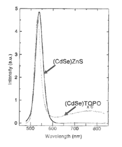
Atomic layer deposition for functionalizing colloidal and semiconductor particles
PatentActiveUS8012860B2
Innovation
- Atomic layer deposition (ALD) is used to replace organic layers with inorganic materials, specifically depositing a selected film layer over colloidal quantum dots to enhance electronic coupling and improve the electronic properties of the nanocomposites, allowing for the creation of functionalized nanocomposites with improved electrical and optical properties.
Materials Science Considerations for ALD-Coated Nanowires
The atomic layer deposition (ALD) coating of nanowires represents a critical intersection of materials science and nanotechnology, where the fundamental properties of materials at the nanoscale significantly influence electrical conductivity outcomes. When applying ALD coatings to enhance nanowire conductivity, several material considerations must be carefully evaluated to achieve optimal performance.
The crystallinity of the coating material plays a decisive role in determining electrical properties. Highly crystalline ALD coatings typically offer superior electron mobility compared to amorphous structures, as they provide more ordered pathways for electron transport. However, the crystallization process must be precisely controlled to prevent defect formation at the nanowire-coating interface, which could otherwise create electron scattering sites.
Interface engineering between the nanowire substrate and the ALD coating represents another crucial consideration. The quality of this interface directly impacts charge transfer efficiency across material boundaries. Chemical compatibility between substrate and coating materials must be evaluated to minimize lattice mismatch and prevent the formation of interfacial oxides or other compounds that could increase contact resistance.
Thickness optimization of ALD coatings presents a delicate balance in conductivity enhancement. While thicker coatings may provide more conductive material, they can also introduce strain in the nanowire structure or create diffusion barriers. Conversely, ultra-thin coatings may not provide sufficient conductive pathways but offer advantages in maintaining nanowire flexibility and optical properties.
Doping strategies within ALD coatings offer powerful mechanisms to tailor electrical conductivity. Controlled introduction of dopants during the ALD process can significantly modify the electronic band structure of coating materials. For metallic coatings, dopants can increase carrier concentration, while for semiconductor coatings, they can shift the Fermi level to enhance conductivity.
Thermal stability considerations are essential for practical applications, as nanowire devices often operate under varying temperature conditions. The coefficient of thermal expansion mismatch between nanowire and coating materials can induce mechanical stress during thermal cycling, potentially leading to delamination or cracking that disrupts electrical pathways.
Surface roughness and morphology control during ALD processing directly influence electron scattering at surfaces. Smoother coatings generally provide better conductivity by reducing surface scattering effects, while maintaining conformality around the complex nanowire geometry remains a technical challenge requiring precise process parameter optimization.
Scalability and Manufacturing Challenges for Industrial Implementation
The industrial implementation of ALD coating for enhancing electrical conductivity in nanowires faces significant scalability and manufacturing challenges that must be addressed before widespread adoption can occur. Current ALD processes, while effective at laboratory scale, often suffer from throughput limitations when scaled to industrial production volumes. The batch processing nature of many ALD systems creates bottlenecks that restrict production rates to levels insufficient for mass-market applications.
Equipment cost represents another substantial barrier, as industrial-grade ALD systems require significant capital investment, often ranging from $500,000 to several million dollars depending on capacity and specifications. This high initial cost creates a considerable entry barrier for smaller manufacturers and startups interested in nanowire technology implementation.
Process time optimization remains problematic at industrial scales. The inherently slow deposition rates of ALD (typically 0.1-1.0 Å per cycle) result in extended processing times that can significantly impact production economics. While this precision is beneficial for quality control, it creates challenges for high-volume manufacturing environments where throughput is paramount.
Uniformity maintenance across large substrate areas presents technical difficulties when scaling up. As substrate dimensions increase, ensuring consistent precursor delivery and reaction conditions becomes increasingly complex. Edge effects and gas flow dynamics can lead to thickness variations that compromise the electrical performance of nanowire networks in large-area applications.
Precursor management introduces additional complications in industrial settings. Many high-performance ALD precursors have limited shelf life, require specialized handling, or pose safety concerns when used in large quantities. The logistics of precursor supply chain management, including storage, delivery, and waste handling, become significantly more complex at industrial scales.
Integration with existing manufacturing lines presents compatibility challenges. ALD processes often require specific environmental conditions (vacuum, temperature control, etc.) that may not align with established production workflows. Retrofitting existing facilities or developing hybrid manufacturing approaches that accommodate ALD steps without disrupting overall production flow requires careful engineering and substantial investment.
Environmental and regulatory considerations also impact scalability, as some ALD precursors may trigger environmental compliance requirements when used at industrial volumes. Waste stream management, emission controls, and worker safety protocols must be developed specifically for large-scale implementation of these specialized coating processes.
Unlock deeper insights with Patsnap Eureka Quick Research — get a full tech report to explore trends and direct your research. Try now!
Generate Your Research Report Instantly with AI Agent
Supercharge your innovation with Patsnap Eureka AI Agent Platform!