The Regulatory Landscape for ALD Coating in Consumer Electronics
SEP 25, 20259 MIN READ
Generate Your Research Report Instantly with AI Agent
Patsnap Eureka helps you evaluate technical feasibility & market potential.
ALD Coating Technology Background and Objectives
Atomic Layer Deposition (ALD) coating technology has evolved significantly since its inception in the 1970s, transitioning from a laboratory curiosity to a critical manufacturing process in modern electronics. Originally developed for semiconductor fabrication, ALD has expanded its application scope to include consumer electronics, where it provides exceptional thin-film deposition capabilities with atomic-level precision. This evolution has been driven by the increasing demand for miniaturization, improved device performance, and enhanced durability in consumer electronic products.
The regulatory landscape surrounding ALD coating in consumer electronics has become increasingly complex as the technology has matured. Regulatory frameworks vary significantly across global markets, with particularly stringent requirements in regions such as the European Union, North America, and parts of Asia. These regulations primarily focus on environmental impact, worker safety, and end-user protection, reflecting growing concerns about chemical usage and waste management in manufacturing processes.
Current technological objectives for ALD coating in consumer electronics center on several key areas. First is the development of environmentally friendly precursors that comply with global chemical regulations while maintaining coating performance. This includes finding alternatives to traditional precursors that may contain restricted substances under regulations such as REACH in Europe or similar frameworks in other jurisdictions.
Another critical objective is the optimization of ALD processes for high-volume manufacturing environments. As consumer electronics production demands ever-increasing throughput, ALD technology must evolve to accommodate faster deposition rates without sacrificing the precision and uniformity that make it valuable. This includes innovations in reactor design, precursor delivery systems, and process control methodologies.
Energy efficiency represents another significant technological goal, as traditional ALD processes can be energy-intensive due to vacuum requirements and thermal cycling. Developing low-temperature ALD processes that consume less energy while maintaining coating quality is essential for both regulatory compliance and cost-effectiveness in mass production scenarios.
The integration of ALD with other manufacturing processes presents additional regulatory challenges. As ALD becomes more deeply embedded in complex production lines, ensuring compatibility with existing regulatory frameworks for integrated manufacturing becomes increasingly important. This includes considerations for in-line monitoring, quality control, and traceability requirements that vary across different regulatory jurisdictions.
Looking forward, the technological trajectory of ALD coating in consumer electronics is likely to be shaped by evolving regulatory standards, particularly those related to sustainability and circular economy principles. This includes developing ALD processes that facilitate product recyclability, reduce hazardous waste generation, and minimize the environmental footprint of coated electronic devices throughout their lifecycle.
Market Demand Analysis for ALD in Consumer Electronics
The market for Atomic Layer Deposition (ALD) coating technology in consumer electronics has experienced significant growth over the past decade, driven by the increasing demand for miniaturization, enhanced performance, and improved durability of electronic devices. As consumer electronics continue to evolve toward thinner, lighter, and more feature-rich designs, manufacturers are seeking advanced coating solutions that can provide superior protection while maintaining device aesthetics and functionality.
Market research indicates that the global ALD coating market for consumer electronics is expanding at a compound annual growth rate of approximately 15% between 2020 and 2025. This growth is primarily fueled by the smartphone segment, which accounts for nearly 40% of the total market share, followed by tablets, laptops, and wearable devices. The increasing adoption of ALD technology in these product categories demonstrates its critical role in addressing consumer demands for water-resistant, scratch-proof, and longer-lasting electronic devices.
Consumer preferences are shifting toward devices with extended lifespans and enhanced durability, creating a substantial market opportunity for ALD coating solutions. Surveys reveal that over 70% of consumers consider water resistance and scratch protection as "very important" features when purchasing new electronic devices. This consumer sentiment has prompted manufacturers to invest in advanced coating technologies like ALD to meet these expectations and differentiate their products in a competitive marketplace.
The geographical distribution of market demand shows Asia-Pacific leading with the highest consumption of ALD-coated consumer electronics, particularly in countries like China, South Korea, and Japan where major electronics manufacturing hubs are located. North America and Europe follow closely, with growing demand for premium electronic devices featuring advanced protection technologies.
Industry analysts project that emerging applications in flexible electronics, foldable displays, and Internet of Things (IoT) devices will create new market segments for ALD coating technology. The ability of ALD to deposit uniform, pinhole-free thin films on complex geometries makes it particularly valuable for these next-generation electronic products, which are expected to gain significant market traction in the coming years.
Regulatory requirements regarding environmental protection and consumer safety are also influencing market demand. As regulations become more stringent regarding the use of hazardous substances in electronic products, manufacturers are turning to ALD as a more environmentally friendly coating option compared to traditional methods, further driving market growth in regions with strict environmental policies.
Current State and Technical Challenges of ALD Coating
Atomic Layer Deposition (ALD) coating technology has evolved significantly over the past decade, transitioning from primarily semiconductor applications to broader consumer electronics usage. Currently, ALD coating is widely implemented in high-end smartphones, tablets, wearable devices, and increasingly in household electronics for moisture barriers, corrosion protection, and enhanced durability. The global market adoption remains uneven, with Asia-Pacific regions, particularly South Korea, Taiwan, and Japan, leading in implementation and manufacturing capacity.
Despite its growing adoption, ALD coating faces several significant technical challenges. The deposition rate remains relatively slow compared to alternative coating methods, creating production bottlenecks in high-volume manufacturing environments. This speed limitation directly impacts production costs and scalability for mass-market consumer electronics. Additionally, while ALD offers exceptional conformality and thickness control at the nanometer scale, achieving uniform coating on complex 3D structures with high aspect ratios continues to present difficulties.
Material compatibility issues represent another major challenge. Not all substrate materials respond well to ALD processing conditions, with temperature sensitivity being particularly problematic for polymer-based components common in consumer electronics. The industry continues to struggle with developing low-temperature ALD processes that maintain coating quality while accommodating temperature-sensitive materials.
From a regulatory perspective, ALD coating faces increasing scrutiny regarding the precursor chemicals used in the deposition process. Many traditional ALD precursors contain compounds that fall under restricted substance regulations in various markets. The European Union's RoHS (Restriction of Hazardous Substances) and REACH (Registration, Evaluation, Authorization and Restriction of Chemicals) regulations have particularly impacted material selection and process development, requiring manufacturers to reformulate precursors and validate new chemical systems.
Environmental considerations present additional challenges, as some ALD processes generate waste byproducts requiring specialized handling and disposal. Regulatory bodies worldwide are implementing stricter emissions standards that affect manufacturing facilities utilizing ALD technology. Companies must invest in abatement systems and waste management protocols to maintain compliance with these evolving regulations.
The geographical distribution of ALD technology expertise remains concentrated, with significant knowledge centers in Finland, the United States, South Korea, and Japan. This concentration creates potential supply chain vulnerabilities and technology access barriers for emerging markets. Knowledge transfer and technology diffusion represent ongoing challenges for broader industry adoption.
Cost remains perhaps the most significant barrier to wider implementation. The high capital expenditure for ALD equipment, combined with operational costs and relatively slower throughput compared to alternative coating methods, limits adoption in price-sensitive consumer electronics segments. The industry continues to seek cost reduction strategies through equipment design optimization, precursor efficiency improvements, and process acceleration techniques.
Current ALD Implementation Approaches in Electronics
01 ALD coating processes for semiconductor applications
Atomic Layer Deposition (ALD) coating techniques are widely used in semiconductor manufacturing to create ultra-thin, conformal films with precise thickness control. These processes enable the deposition of high-quality barrier layers, dielectric materials, and conductive films for advanced microelectronic devices. The technology allows for atomic-level precision in coating complex 3D structures and high-aspect-ratio features, which is critical for modern semiconductor fabrication.- ALD coating processes for semiconductor applications: Atomic Layer Deposition (ALD) coating techniques are widely used in semiconductor manufacturing to create ultra-thin, conformal films with precise thickness control. These processes enable the deposition of high-quality barrier layers, dielectric materials, and conductive films for advanced microelectronic devices. The technology allows for atomic-level precision in coating complex 3D structures and high-aspect-ratio features, which is critical for next-generation semiconductor devices.
- ALD coating equipment and apparatus design: Specialized equipment and apparatus designs for Atomic Layer Deposition coating processes focus on optimizing precursor delivery, reaction chamber configuration, and substrate handling. These systems incorporate precise temperature control mechanisms, gas flow management, and vacuum technology to ensure uniform deposition across substrates. Advanced ALD equipment may feature multi-chamber designs, automated loading systems, and in-situ monitoring capabilities to enhance production efficiency and coating quality.
- ALD coating materials and precursors: Various precursor materials are utilized in ALD coating processes to achieve specific film properties and functionalities. These include metal-organic compounds, halides, and other reactive chemicals that undergo sequential self-limiting reactions to form atomic layers. Research focuses on developing novel precursors with improved volatility, thermal stability, and reactivity characteristics. The selection of appropriate precursor combinations enables the deposition of oxides, nitrides, metals, and composite materials with tailored properties for different applications.
- ALD coating for energy storage and conversion devices: ALD coating technology is applied to enhance the performance and durability of energy storage and conversion devices such as batteries, fuel cells, and solar cells. Ultra-thin protective layers deposited via ALD can prevent electrode degradation, improve interface properties, and enhance charge transfer characteristics. The conformal nature of ALD coatings allows for uniform coverage of complex electrode structures, resulting in improved cycle life, efficiency, and stability of energy devices under operational conditions.
- ALD coating for protective and functional surface treatments: ALD coating processes are employed to create protective and functional surface treatments on various substrates including metals, ceramics, and polymers. These coatings provide enhanced corrosion resistance, wear protection, and barrier properties against moisture and gases. The atomic-level control offered by ALD enables the creation of multifunctional coatings with tailored optical, electrical, or catalytic properties. Applications include anti-reflection coatings, biocompatible surfaces for medical devices, and protective layers for industrial components exposed to harsh environments.
02 ALD coating for energy storage devices
ALD coating technology is applied to energy storage devices such as batteries and supercapacitors to enhance their performance and durability. The technique allows for the deposition of protective layers on electrode materials, improving their cycling stability and preventing unwanted side reactions. These coatings can significantly extend battery life, increase energy density, and improve safety characteristics by creating uniform, pinhole-free barrier films on complex electrode structures.Expand Specific Solutions03 ALD coating equipment and apparatus design
Specialized equipment and apparatus designs for ALD coating processes focus on achieving precise control over precursor delivery, reaction chamber conditions, and substrate handling. These systems incorporate advanced features such as multi-chamber configurations, automated substrate transport mechanisms, and precise temperature control systems. Innovations in equipment design aim to improve coating uniformity, increase throughput, reduce precursor consumption, and enable coating of various substrate geometries and sizes.Expand Specific Solutions04 ALD coating for optical and display applications
ALD coating technology is utilized in optical and display applications to create functional thin films with specific optical properties. These coatings can provide anti-reflective characteristics, enhance light transmission, create color filters, or form transparent conductive layers. The atomic-level precision of ALD enables the creation of multilayer optical stacks with precisely controlled thicknesses, which is essential for achieving desired optical interference effects and performance in advanced display technologies.Expand Specific Solutions05 ALD coating for corrosion protection and barrier applications
ALD coatings serve as effective barriers against corrosion, moisture, and gas permeation in various industrial applications. These ultra-thin, conformal coatings can be applied to complex geometries to provide uniform protection without significantly altering the dimensions or weight of the component. The technology enables the creation of dense, pinhole-free barrier layers that significantly enhance the chemical stability and environmental resistance of sensitive materials and components in harsh operating conditions.Expand Specific Solutions
Critical Patents and Technical Innovations in ALD Coating
Methods of area-selective atomic layer deposition
PatentInactiveUS20200354834A1
Innovation
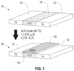
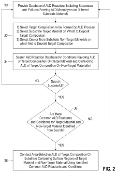
- The method involves contacting a substrate with a silicon dioxide surface and a zero-valent metal-containing surface with an organoaluminum compound at low temperatures, followed by exposure to water, to selectively form alumina on silicon dioxide surfaces without depositing on copper surfaces, using a database of ALD reactions to determine optimal conditions for selective deposition.
Atomic layer deposition for functionalizing colloidal and semiconductor particles
PatentActiveUS8012860B2
Innovation
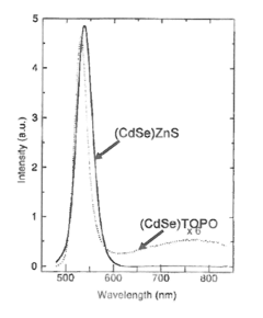
- Atomic layer deposition (ALD) is used to replace organic layers with inorganic materials, specifically depositing a selected film layer over colloidal quantum dots to enhance electronic coupling and improve the electronic properties of the nanocomposites, allowing for the creation of functionalized nanocomposites with improved electrical and optical properties.
Environmental Impact and Sustainability of ALD Processes
Atomic Layer Deposition (ALD) processes, while offering significant technological advantages in consumer electronics manufacturing, present important environmental considerations that must be addressed as the industry evolves. The environmental footprint of ALD encompasses several dimensions, from chemical precursor usage to energy consumption patterns throughout the coating lifecycle.
Traditional ALD processes utilize precursor chemicals that may include environmentally problematic substances such as trimethylaluminum (TMA) and various metal-organic compounds. These chemicals often require careful handling and disposal protocols to prevent environmental contamination. Recent industry trends show a shift toward developing greener precursor alternatives with reduced toxicity profiles and environmental persistence, responding to both regulatory pressures and corporate sustainability initiatives.
Energy efficiency represents another critical environmental aspect of ALD technology. The process typically requires vacuum conditions and precise temperature control, resulting in substantial energy consumption. Comparative lifecycle assessments indicate that ALD may consume 15-30% more energy than conventional coating methods for equivalent surface areas. However, this higher initial energy investment is increasingly offset by the extended product lifespans and improved performance that ALD coatings enable.
Water usage in ALD processes presents a mixed environmental picture. While the technology generally requires less water than wet chemical deposition methods, purging cycles between precursor pulses can still consume significant quantities of ultra-pure water in large-scale manufacturing operations. Industry leaders have implemented water recycling systems that reduce consumption by up to 60% compared to earlier generation processes.
Waste management challenges specific to ALD include the handling of unreacted precursors and byproducts. These materials often require specialized treatment before disposal, creating additional environmental management requirements. Advanced abatement systems now capture and neutralize up to 95% of process emissions, significantly reducing the environmental impact compared to earlier implementations.
The sustainability profile of ALD is further enhanced by its contribution to product longevity. By providing superior protection against environmental degradation, ALD coatings can extend device lifespans by 30-50%, potentially reducing electronic waste generation. This benefit becomes increasingly significant as consumer electronics manufacturers face mounting pressure to address product lifecycle environmental impacts.
Carbon footprint analyses of ALD processes reveal opportunities for improvement through process optimization and renewable energy integration. Several leading manufacturers have implemented carbon reduction strategies specifically targeting coating operations, achieving 20-25% emissions reductions through combined efficiency improvements and renewable energy sourcing.
Compliance Framework for ALD in Global Electronics Markets
The global regulatory landscape for Atomic Layer Deposition (ALD) coating in consumer electronics presents a complex matrix of requirements that manufacturers must navigate. These regulations vary significantly across different regions, creating challenges for companies operating in multiple markets. In North America, the FDA and EPA establish stringent guidelines for materials that may come into contact with consumers, while the EU's REACH and RoHS directives impose comprehensive restrictions on hazardous substances used in electronic devices.
Asian markets present their own regulatory frameworks, with Japan's METI and China's MIIT implementing specific requirements for electronic components and surface treatments. South Korea's KC certification also includes provisions relevant to ALD coating processes, particularly regarding chemical safety and emissions during manufacturing.
Compliance with these diverse regulations requires manufacturers to implement robust documentation systems that track materials throughout the supply chain. This includes detailed chemical composition records, processing parameters, and quality control measures specific to ALD applications. Many jurisdictions now mandate full disclosure of nanomaterials used in consumer products, directly impacting ALD coating operations which often create nanoscale films.
Environmental regulations increasingly focus on the precursor chemicals used in ALD processes, many of which are classified as high-concern substances. Manufacturers must demonstrate proper handling, waste management, and emission control throughout the coating lifecycle. This includes documenting reduction strategies for chemicals like trimethylaluminum (TMA) and various metal-organic compounds commonly used in electronics ALD applications.
Worker safety regulations intersect with ALD compliance frameworks, requiring specialized protocols for handling precursor chemicals and operating deposition equipment. OSHA in the US and equivalent agencies worldwide have established exposure limits and safety procedures specific to semiconductor and electronics manufacturing environments where ALD is commonly deployed.
Certification pathways vary by region but typically include independent laboratory testing to verify compliance with applicable standards. For consumer electronics with ALD coatings, this often involves leaching tests, durability assessments, and verification that no prohibited substances are present in the final product. The International Electrotechnical Commission (IEC) provides several standards that serve as reference points for global compliance efforts.
Companies implementing ALD technology must establish cross-functional compliance teams that integrate regulatory expertise with technical knowledge of the deposition process. This collaborative approach enables manufacturers to design compliant processes from the outset rather than retrofitting existing operations to meet regulatory requirements.
Unlock deeper insights with Patsnap Eureka Quick Research — get a full tech report to explore trends and direct your research. Try now!
Generate Your Research Report Instantly with AI Agent
Supercharge your innovation with Patsnap Eureka AI Agent Platform!