Comparison of ALD Coating vs. CVD Coating in Nano-Fabrication
SEP 25, 20259 MIN READ
Generate Your Research Report Instantly with AI Agent
Patsnap Eureka helps you evaluate technical feasibility & market potential.
ALD and CVD Nano-Coating Evolution and Objectives
Atomic Layer Deposition (ALD) and Chemical Vapor Deposition (CVD) represent two cornerstone technologies in the evolution of nano-fabrication processes. Tracing back to the 1960s, CVD emerged as a pioneering method for thin film deposition, while ALD's conceptual foundations were established in the 1970s under the initial name "Atomic Layer Epitaxy" by Finnish scientist Tuomo Suntola. The technological trajectory of these coating methodologies has been characterized by continuous refinement to meet increasingly stringent requirements for precision engineering at the nanoscale.
The evolution of ALD technology has been particularly remarkable, transitioning from specialized applications in electroluminescent displays to becoming an indispensable process in semiconductor manufacturing. This progression was catalyzed by the semiconductor industry's relentless pursuit of miniaturization, as articulated in Moore's Law, which necessitated coating technologies capable of atomic-level precision. CVD, meanwhile, evolved from conventional thermal processes to include plasma-enhanced variants (PECVD) and metal-organic precursor systems (MOCVD), expanding its versatility across diverse industrial applications.
Recent technological advancements have significantly enhanced both methodologies. ALD has benefited from innovations in precursor chemistry and reactor design, enabling lower processing temperatures and higher throughput—historically limiting factors for industrial adoption. Concurrently, CVD technology has advanced through improved process control systems and in-situ monitoring capabilities, allowing for more precise manipulation of film properties and composition.
The primary objective in comparing these technologies is to establish a comprehensive framework for evaluating their respective advantages in nano-fabrication contexts. This includes assessing conformality on high-aspect-ratio structures, thickness uniformity across large substrates, material quality metrics (density, impurity levels, crystallinity), and process integration considerations. Additionally, this analysis aims to identify application-specific optimization strategies that leverage the unique capabilities of each technology.
Looking forward, the technological roadmap for both ALD and CVD is increasingly focused on enabling emerging applications in flexible electronics, energy storage systems, and quantum computing. These applications present novel challenges that will drive further innovation in precursor chemistry, process integration, and equipment design. The ultimate goal is to develop a predictive understanding of how these coating technologies can be strategically deployed to enable next-generation nano-engineered materials and devices with unprecedented performance characteristics.
Market Demand Analysis for Nano-Fabrication Coatings
The global market for nano-fabrication coatings has experienced significant growth in recent years, driven by increasing demands across multiple industries including semiconductor manufacturing, medical devices, energy storage, and optical applications. The market value for advanced thin film deposition technologies reached approximately $12 billion in 2022, with projections indicating a compound annual growth rate of 8.7% through 2028.
Atomic Layer Deposition (ALD) and Chemical Vapor Deposition (CVD) technologies represent critical segments within this market. The ALD coating market specifically has shown accelerated growth at 15.3% annually, outpacing traditional CVD methods which maintain steady growth at 6.2%. This differential growth rate reflects the increasing technical requirements for precision coating at the nanoscale level.
The semiconductor industry remains the largest consumer of nano-fabrication coatings, accounting for 43% of the total market. The continuous miniaturization of electronic components, following Moore's Law, has created substantial demand for atomic-level precision in coating technologies. High-k dielectric materials deposited via ALD have become essential for advanced logic and memory devices, with the market for these applications growing at 17.8% annually.
Medical and biomedical applications represent the fastest-growing segment for nano-fabrication coatings, with a 22.4% annual growth rate. The demand is primarily driven by requirements for biocompatible coatings on implantable devices and precision drug delivery systems. ALD's ability to create ultra-thin, conformal coatings on complex geometries has positioned it as the preferred technology in this sector.
Energy storage and conversion applications, particularly in battery technology and solar cells, constitute another significant market segment. The demand for precise interface engineering in these applications has grown by 19.6% annually, with both ALD and CVD technologies competing for market share based on specific application requirements.
Regional analysis indicates that Asia-Pacific dominates the market with 58% share, led by manufacturing hubs in Taiwan, South Korea, and China. North America follows with 24% market share, with particularly strong demand in medical and aerospace applications. Europe accounts for 16% of the market, with significant research activities driving innovation in coating technologies.
Customer requirements are increasingly focused on achieving greater precision, uniformity, and lower defect rates in nano-scale coatings. Industry surveys indicate that 76% of end-users prioritize coating quality over processing speed, while 68% are actively seeking technologies that can reduce material consumption and environmental impact. This trend favors ALD technology in applications requiring atomic-level precision, while CVD maintains advantages in higher-throughput scenarios.
Current State and Technical Barriers in Nano-Coating Technologies
Nano-coating technologies have witnessed significant advancements in recent years, with Atomic Layer Deposition (ALD) and Chemical Vapor Deposition (CVD) emerging as dominant methodologies. Currently, these technologies face several technical challenges that limit their widespread industrial application despite their promising capabilities in creating uniform, conformal coatings at the nanoscale.
The global landscape of nano-coating technologies reveals regional disparities in development and implementation. North America and East Asia, particularly Japan and South Korea, lead in ALD technology advancement, while Europe demonstrates strength in specialized CVD applications. China has rapidly expanded its capabilities in both technologies but still lags in proprietary innovation for high-precision applications.
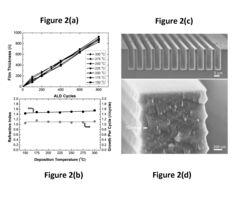
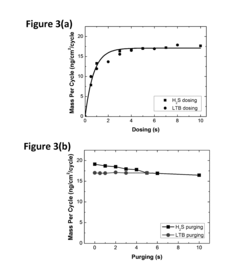
ALD coating technology currently excels in producing ultra-thin films with precise thickness control down to the angstrom level, achieving exceptional conformality even on complex 3D structures. However, it faces significant barriers including slow deposition rates (typically 0.1-0.2 nm/cycle), limiting industrial throughput and increasing production costs. Additionally, the limited availability of suitable precursors for certain materials restricts application diversity.
CVD coating, while offering faster deposition rates and broader material compatibility, struggles with achieving the same level of precision as ALD in thickness uniformity. Technical challenges include difficulty in controlling film composition in multi-component systems and higher process temperatures that can damage temperature-sensitive substrates. The complex reaction kinetics in CVD processes also create reproducibility issues in large-scale manufacturing environments.
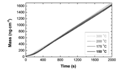
Both technologies face common challenges in scaling to larger substrate sizes while maintaining coating quality. Energy consumption remains high, particularly for CVD processes that typically operate at elevated temperatures (600-1000°C), whereas ALD generally requires lower temperatures (150-350°C) but longer processing times.
Integration challenges persist when incorporating these nano-coating technologies into existing manufacturing lines, requiring significant process optimization and equipment modifications. The semiconductor industry has made substantial progress in this integration, but other sectors like medical devices and energy storage face steeper adoption curves.
Material compatibility issues represent another significant barrier, especially when coating polymers or biological materials that cannot withstand vacuum conditions or elevated temperatures. Recent developments in plasma-enhanced variants of both technologies have partially addressed these limitations but introduced new complexities in process control.
Quality control and characterization of nano-coatings present ongoing challenges, as conventional metrology tools struggle to accurately measure properties of ultra-thin films, particularly on complex geometries. This limitation hampers process optimization and quality assurance in production environments.
The global landscape of nano-coating technologies reveals regional disparities in development and implementation. North America and East Asia, particularly Japan and South Korea, lead in ALD technology advancement, while Europe demonstrates strength in specialized CVD applications. China has rapidly expanded its capabilities in both technologies but still lags in proprietary innovation for high-precision applications.
ALD coating technology currently excels in producing ultra-thin films with precise thickness control down to the angstrom level, achieving exceptional conformality even on complex 3D structures. However, it faces significant barriers including slow deposition rates (typically 0.1-0.2 nm/cycle), limiting industrial throughput and increasing production costs. Additionally, the limited availability of suitable precursors for certain materials restricts application diversity.
CVD coating, while offering faster deposition rates and broader material compatibility, struggles with achieving the same level of precision as ALD in thickness uniformity. Technical challenges include difficulty in controlling film composition in multi-component systems and higher process temperatures that can damage temperature-sensitive substrates. The complex reaction kinetics in CVD processes also create reproducibility issues in large-scale manufacturing environments.
Both technologies face common challenges in scaling to larger substrate sizes while maintaining coating quality. Energy consumption remains high, particularly for CVD processes that typically operate at elevated temperatures (600-1000°C), whereas ALD generally requires lower temperatures (150-350°C) but longer processing times.
Integration challenges persist when incorporating these nano-coating technologies into existing manufacturing lines, requiring significant process optimization and equipment modifications. The semiconductor industry has made substantial progress in this integration, but other sectors like medical devices and energy storage face steeper adoption curves.
Material compatibility issues represent another significant barrier, especially when coating polymers or biological materials that cannot withstand vacuum conditions or elevated temperatures. Recent developments in plasma-enhanced variants of both technologies have partially addressed these limitations but introduced new complexities in process control.
Quality control and characterization of nano-coatings present ongoing challenges, as conventional metrology tools struggle to accurately measure properties of ultra-thin films, particularly on complex geometries. This limitation hampers process optimization and quality assurance in production environments.
Comparative Analysis of Current ALD and CVD Implementation Approaches
01 Comparison of ALD and CVD coating technologies
Atomic Layer Deposition (ALD) and Chemical Vapor Deposition (CVD) are two distinct thin film deposition techniques with different characteristics. ALD offers precise thickness control through self-limiting reactions that deposit one atomic layer at a time, resulting in highly conformal coatings even on complex geometries. CVD typically provides higher deposition rates but with less precise thickness control. The choice between these technologies depends on specific application requirements such as conformality needs, deposition rate, and film quality.- Comparison of ALD and CVD coating technologies: Atomic Layer Deposition (ALD) and Chemical Vapor Deposition (CVD) are both thin film deposition techniques used in semiconductor manufacturing and other applications. ALD offers precise thickness control through self-limiting surface reactions, depositing one atomic layer at a time, while CVD involves continuous chemical reactions at the substrate surface. ALD typically provides better conformality and uniformity for complex geometries, whereas CVD generally offers higher deposition rates. These technologies are often selected based on specific application requirements for film quality, deposition rate, and process temperature.
- Precursors and reaction mechanisms for ALD/CVD processes: The selection of precursors is critical in both ALD and CVD processes, determining film properties and process efficiency. For ALD, precursors must have high volatility, thermal stability, and reactivity with surface sites but not with themselves. Common precursors include metal-organic compounds, halides, and various reactive gases. The reaction mechanisms involve sequential, self-limiting surface reactions with purge steps between exposures. For CVD, precursors undergo gas-phase and surface reactions simultaneously, requiring careful control of temperature, pressure, and gas flow to achieve desired film properties and minimize defects.
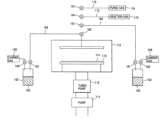
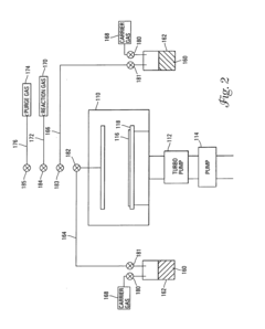
- Equipment and reactor designs for ALD/CVD processes: Specialized equipment and reactor designs are essential for effective ALD and CVD processes. ALD reactors typically feature rapid gas switching capabilities, uniform gas distribution systems, and precise temperature control. CVD reactors may include hot-wall or cold-wall designs, with various configurations such as horizontal, vertical, or barrel reactors. Advanced systems incorporate in-situ monitoring tools for real-time process control. Recent innovations include spatial ALD systems for higher throughput and hybrid ALD/CVD reactors that combine benefits of both techniques. Equipment design considerations include precursor delivery systems, vacuum components, and heating elements optimized for specific applications.
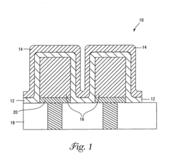
- Applications of ALD/CVD coatings in semiconductor manufacturing: ALD and CVD coatings play crucial roles in semiconductor manufacturing, particularly as device dimensions continue to shrink. These techniques are used to deposit high-k dielectric materials, diffusion barriers, gate electrodes, and interconnect structures. ALD is particularly valuable for ultra-thin conformal films in high-aspect-ratio structures like FinFETs, deep trenches, and 3D NAND memory. CVD processes are widely employed for depositing silicon dioxide, silicon nitride, and various metal films. Both technologies enable critical steps in advanced node fabrication, including front-end-of-line and back-end-of-line processes, contributing to improved device performance and reliability.
- Novel materials and emerging applications for ALD/CVD coatings: Research in ALD and CVD is expanding to novel materials and emerging applications beyond traditional semiconductor manufacturing. These include conformal coatings for energy storage devices like batteries and supercapacitors, protective layers for MEMS/NEMS devices, and functional films for optical applications. ALD enables precise deposition of nanolaminates and doped materials with tailored properties. Low-temperature ALD and CVD processes are being developed for temperature-sensitive substrates like polymers and biomaterials. Other emerging applications include catalysts, sensors, and quantum computing components, where atomic-level precision in film composition and thickness is critical for performance.
02 ALD precursors and reaction mechanisms
The effectiveness of ALD coating processes heavily depends on the selection of appropriate precursors and understanding their reaction mechanisms. Various metal-organic compounds, halides, and other reactive species are used as precursors in ALD. These precursors must have sufficient volatility, thermal stability, and reactivity to ensure complete surface reactions while preventing unwanted CVD-like growth. The sequential, self-limiting nature of ALD reactions enables precise control over film composition and properties, with each cycle typically consisting of precursor exposure, purge, reactant exposure, and another purge step.Expand Specific Solutions03 Equipment and apparatus for ALD and CVD processes
Specialized equipment and apparatus are essential for both ALD and CVD coating processes. These systems typically include precursor delivery systems, reaction chambers, temperature control mechanisms, and exhaust handling components. ALD systems require precise gas flow control and rapid switching capabilities to achieve the sequential exposure necessary for layer-by-layer growth. CVD equipment often focuses on optimizing gas flow dynamics and temperature uniformity across the substrate. Advanced systems may incorporate features such as plasma enhancement, hot-wall or cold-wall designs, and in-situ monitoring capabilities to improve coating quality and process control.Expand Specific Solutions04 Applications of ALD and CVD coatings in semiconductor manufacturing
ALD and CVD coating technologies play crucial roles in semiconductor manufacturing, particularly as device dimensions continue to shrink. ALD is especially valuable for depositing ultra-thin, conformal films for high-aspect-ratio structures like trenches and vias in advanced logic and memory devices. Applications include high-k dielectric layers, diffusion barriers, and metal electrodes. CVD processes are widely used for depositing thicker films such as interlayer dielectrics, passivation layers, and certain metal films. The selection between ALD and CVD depends on specific requirements for film thickness, conformality, throughput, and material properties in the semiconductor fabrication process.Expand Specific Solutions05 Novel materials and multi-layer structures by ALD and CVD
Advanced ALD and CVD techniques enable the deposition of novel materials and complex multi-layer structures with precisely controlled compositions and interfaces. These include nanolaminate structures, doped films, and mixed-phase materials with tailored properties. ALD's ability to deposit conformal films one atomic layer at a time makes it particularly suitable for creating sophisticated stacks with sharp interfaces. CVD processes can be optimized to deposit functional gradient materials and complex compounds. These capabilities are leveraged in applications ranging from optical coatings and protective barriers to energy storage materials and catalytic surfaces, where precise control over composition and structure is critical for performance.Expand Specific Solutions
Leading Companies and Research Institutions in Nano-Coating Industry
The ALD vs. CVD coating market in nano-fabrication is currently in a growth phase, with the global market expected to reach significant expansion due to increasing demand for precise thin film deposition technologies. ALD technology offers superior conformality and thickness control at atomic scale compared to traditional CVD, making it increasingly preferred for advanced applications. Leading players like Applied Materials, ASM International, and Tokyo Electron have established strong technological foundations in both methods, while companies such as Picosun and Beneq have specialized in ALD innovations. Taiwan Semiconductor Manufacturing Co. and IBM represent major end-users driving adoption. The competitive landscape shows established semiconductor equipment manufacturers expanding their portfolios while specialized ALD providers focus on niche applications, creating a dynamic market with ongoing technological advancement and increasing industrial adoption.
Applied Materials, Inc.
Technical Solution: Applied Materials has developed comprehensive solutions for both ALD and CVD technologies in nanofabrication. Their Endura® platform integrates ALD capabilities for ultra-thin conformal films with atomic-level precision. For high-volume manufacturing, Applied Materials' Producer® XP system offers advanced CVD processes with enhanced throughput. Their ALD technology achieves conformal coating on structures with aspect ratios exceeding 60:1, while maintaining thickness variation below 2%[2]. Applied Materials has pioneered selective deposition techniques that combine aspects of both ALD and CVD, allowing targeted material placement only where needed. Their systems enable the deposition of a wide range of materials including high-k dielectrics, metal gates, and diffusion barriers. The company's CVD technology delivers deposition rates up to 100 times faster than ALD, while their ALD solutions provide superior conformality for sub-10nm features. Applied Materials has also developed hybrid approaches that leverage the advantages of both technologies for specific applications.
Strengths: Comprehensive portfolio spanning both ALD and CVD technologies; high-volume manufacturing capability; advanced process control systems; extensive material library; integrated solutions for complex process flows. Weaknesses: Higher capital equipment costs; some processes require specialized precursors with limited suppliers; certain ALD applications face throughput challenges compared to traditional techniques.
Micron Technology, Inc.
Technical Solution: Micron Technology has implemented specialized ALD and CVD processes for advanced memory fabrication. Their approach to ALD focuses on high-k dielectric materials for DRAM capacitors and 3D NAND structures, achieving exceptional conformality in high-aspect-ratio features. Micron's ALD technology enables precise deposition of ultra-thin films (1-10nm) with thickness control at the sub-angstrom level, critical for maintaining electrical properties in scaled memory devices. For their 3D NAND technology, Micron employs ALD to create uniform dielectric layers in vertical channel structures with aspect ratios exceeding 40:1[3]. Their CVD processes are optimized for higher throughput deposition of thicker films where atomic-level precision is less critical. Micron has developed hybrid approaches that leverage ALD's conformality for critical interfaces while using CVD for bulk film growth, optimizing both performance and production efficiency. Their research indicates ALD processes achieve >95% step coverage in their most challenging structures, compared to 60-80% for optimized CVD processes.
Strengths: Highly optimized processes for memory-specific applications; excellent conformality in extreme aspect ratio structures; precise thickness control for critical electrical properties; integration expertise for complex 3D structures. Weaknesses: Processes highly specialized for memory applications; slower deposition rates for ALD compared to traditional techniques; higher cost per wafer for some applications; requires specialized precursor chemistry.
Critical Patents and Breakthroughs in Nano-Coating Technologies
Materials for solid state electrolytes and protective electrode coatings for lithium batteries
PatentActiveUS20150364747A1
Innovation
- Atomic Layer Deposition (ALD) is used to produce thin, conformal metal sulfide films for lithium-ion and lithium-sulfur batteries, enabling precise control over film thickness and composition, enhancing lithium ion and electronic conductivities, and infiltrating porous electrodes for improved performance.
Systems and methods for forming strontium-and/or barium-containing layers
PatentActiveUS20080210157A9
Innovation
- The use of Group IIA metal diorganoamide precursor compounds, Group VB metal precursor compounds, and optionally titanium precursor compounds in a multi-cycle atomic layer deposition process, with reaction gases like water vapor, to form metal-containing layers such as barium tantalates, strontium niobates, and mixed-metal oxides, which serve as dielectric layers, offering improved conformality and thickness control.
Environmental Impact and Sustainability of Nano-Coating Processes
The environmental impact of nano-coating processes has become increasingly significant as these technologies gain wider industrial adoption. ALD (Atomic Layer Deposition) and CVD (Chemical Vapor Deposition) processes differ substantially in their environmental footprints, with important implications for sustainability in advanced manufacturing.
ALD demonstrates notable environmental advantages through its precise material utilization. The self-limiting reaction mechanism ensures that precursors react only with surface sites, resulting in minimal waste generation compared to CVD processes. Studies indicate that ALD typically achieves 80-95% precursor utilization efficiency, whereas conventional CVD methods often operate at 20-40% efficiency. This difference translates directly to reduced chemical waste and lower environmental contamination potential.
Energy consumption represents another critical environmental factor. CVD processes generally require higher operating temperatures (often 600-900°C) and continuous gas flows, resulting in substantial energy demands. In contrast, ALD can operate at lower temperatures (typically 100-350°C for many applications) with pulsed precursor delivery, reducing overall energy requirements by 30-50% for comparable coating applications. This energy efficiency directly correlates to reduced carbon emissions when considering full lifecycle impacts.
Precursor chemistry also differentiates these technologies from a sustainability perspective. Traditional CVD often employs metal-organic compounds containing environmentally problematic elements like chlorine or fluorine. Modern ALD development has focused on creating more environmentally benign precursors, including water-based systems and non-halogenated compounds. However, both technologies still frequently utilize reactive gases that require careful handling and abatement systems.
Waste management infrastructure represents a significant sustainability challenge for both coating methods. CVD generates larger volumes of particulate waste and unreacted precursors requiring treatment, while ALD produces less waste but may involve more specialized compounds. Advanced facilities have implemented closed-loop recycling systems for precursor recovery, though these remain the exception rather than standard practice across the industry.
Regulatory frameworks increasingly influence adoption decisions, with stricter environmental standards favoring ALD's precision approach. The European Union's REACH regulations and similar global initiatives have accelerated research into greener precursor chemistries and more efficient delivery systems. Leading manufacturers have begun publishing sustainability metrics for their coating processes, creating market pressure for continuous environmental improvement.
Water usage presents another environmental consideration, with CVD typically requiring more extensive cooling systems and wet scrubbers for emissions control. ALD's lower operating temperatures and reduced waste streams generally translate to 40-60% lower water consumption across comparable applications, an increasingly important factor in water-stressed manufacturing regions.
Cost-Benefit Analysis of ALD vs. CVD in Industrial Applications
When evaluating the economic viability of ALD versus CVD technologies in industrial applications, initial equipment investment represents a significant consideration. ALD systems typically require higher capital expenditure than comparable CVD equipment, with high-throughput industrial ALD systems ranging from $500,000 to over $2 million. CVD systems generally cost between $300,000 and $1.5 million, depending on chamber size and process capabilities.
Operational costs present another critical dimension for comparison. ALD processes consume fewer precursor materials due to their self-limiting nature, potentially reducing material costs by 15-30% compared to CVD. However, ALD cycle times are considerably longer, resulting in lower throughput for high-volume manufacturing scenarios. This throughput limitation can increase the effective cost per coated component, particularly in mass production environments.
Energy consumption patterns differ significantly between these technologies. CVD typically operates at higher temperatures (600-1100°C) compared to ALD (150-350°C for most applications), resulting in 25-40% higher energy costs for CVD operations. This temperature differential also impacts substrate compatibility and potential thermal damage risks.
Maintenance requirements and system downtime create additional cost implications. ALD systems generally demonstrate longer mean-time-between-failures due to less aggressive deposition conditions and reduced thermal cycling stress. Industry data suggests ALD systems may require 15-20% less maintenance expenditure annually compared to equivalent CVD systems.
Film quality economics must be considered within specific application contexts. ALD's superior conformality and thickness control often translate to enhanced product performance and reliability, potentially justifying its higher processing costs through reduced failure rates and extended product lifespans. For applications requiring ultra-thin films (<10nm) with precise thickness control, ALD typically delivers a positive return on investment despite higher initial costs.
Scalability economics favor different technologies depending on production volume and coating requirements. CVD demonstrates better cost efficiency at very high volumes for thicker films (>100nm), while ALD becomes increasingly economical for nanoscale applications requiring precise atomic-level control. Recent advancements in spatial ALD have improved throughput by 3-5x compared to traditional ALD, narrowing this economic gap.
Regulatory compliance and environmental considerations also impact the total cost of ownership. ALD typically generates fewer waste byproducts and operates at lower temperatures, potentially reducing environmental compliance costs by 10-25% compared to traditional CVD processes in regions with stringent emissions regulations.
Unlock deeper insights with Patsnap Eureka Quick Research — get a full tech report to explore trends and direct your research. Try now!
Generate Your Research Report Instantly with AI Agent
Supercharge your innovation with Patsnap Eureka AI Agent Platform!