Study of ALD Coating Application in Thin Film Transistor Production
SEP 25, 20259 MIN READ
Generate Your Research Report Instantly with AI Agent
Patsnap Eureka helps you evaluate technical feasibility & market potential.
ALD Technology Evolution and Objectives
Atomic Layer Deposition (ALD) technology has evolved significantly since its inception in the 1970s, transforming from a niche laboratory technique to a critical manufacturing process in semiconductor and electronics industries. Initially developed as a variant of Chemical Vapor Deposition (CVD), ALD distinguished itself through its unique self-limiting surface reactions that enable atomic-level precision in thin film deposition. This characteristic has made ALD particularly valuable for creating ultra-thin, highly conformal coatings on complex three-dimensional structures.
The evolution of ALD technology has been closely tied to the miniaturization trends in electronics, particularly in transistor fabrication. As device dimensions have shrunk below 10nm, conventional deposition methods have reached their physical limitations, creating an opportunity for ALD to address critical challenges in thin film transistor (TFT) production. The technology's ability to deposit uniform layers with thickness control at the angstrom level has become increasingly essential for maintaining electrical performance in advanced semiconductor devices.
Recent advancements in ALD technology have focused on expanding material options beyond traditional metal oxides to include metals, nitrides, sulfides, and organic-inorganic hybrid materials. This material versatility has broadened ALD's application scope in TFT manufacturing, enabling the creation of novel device architectures and improved performance characteristics. Additionally, innovations in plasma-enhanced ALD (PEALD) and spatial ALD have addressed throughput limitations, making the technology more commercially viable for high-volume manufacturing environments.
The primary objective of ALD coating application in TFT production is to achieve precise control over critical thin film properties, including thickness uniformity, conformality, and interface quality. These factors directly influence transistor performance metrics such as carrier mobility, threshold voltage stability, and leakage current. By optimizing these parameters, ALD aims to enable the next generation of high-performance, energy-efficient display technologies and flexible electronics.
Another key objective is to develop low-temperature ALD processes compatible with temperature-sensitive substrates like polymers and organic materials. This capability is crucial for emerging applications in flexible displays, wearable electronics, and large-area electronics where traditional high-temperature deposition methods cannot be employed. Research efforts are increasingly focused on precursor chemistry and reactor design innovations that maintain film quality while reducing thermal budget requirements.
Looking forward, the technology roadmap for ALD in TFT production aims to address challenges related to throughput enhancement, cost reduction, and integration with other manufacturing processes. The industry is also exploring area-selective deposition capabilities to enable bottom-up patterning approaches that could potentially simplify process flows and reduce manufacturing steps. These evolutionary paths align with broader semiconductor industry trends toward more efficient, sustainable production methods for next-generation electronic devices.
TFT Market Demand Analysis
The global Thin Film Transistor (TFT) market has experienced substantial growth in recent years, driven primarily by the expanding display industry. As of 2023, the TFT market is valued at approximately 120 billion USD, with projections indicating a compound annual growth rate (CAGR) of 7.8% through 2028. This growth trajectory is underpinned by increasing consumer demand for high-resolution displays in smartphones, tablets, televisions, and emerging applications such as flexible displays and transparent electronics.
The demand for TFT technology is particularly strong in the consumer electronics sector, which accounts for over 60% of the total market share. Within this segment, smartphones and tablets represent the largest application areas, followed by televisions and computer monitors. The automotive industry has also emerged as a significant growth driver, with in-vehicle displays becoming increasingly sophisticated and prevalent.
Geographically, Asia-Pacific dominates the TFT market, accounting for approximately 70% of global production. This regional concentration is attributed to the presence of major display manufacturers in countries like South Korea, Japan, China, and Taiwan. North America and Europe follow as significant markets, primarily driven by high consumer purchasing power and technological innovation.
The integration of Atomic Layer Deposition (ALD) coating in TFT production has emerged as a critical factor in meeting evolving market demands. End-users increasingly require displays with higher resolution, improved energy efficiency, and enhanced durability. ALD technology addresses these requirements by enabling the deposition of ultra-thin, uniform, and defect-free films that significantly improve TFT performance characteristics.
Market research indicates that manufacturers capable of implementing advanced ALD coating processes can command premium pricing, with consumers willing to pay 15-20% more for devices featuring superior display quality. This price premium underscores the market's recognition of the value added by ALD technology in TFT production.
The COVID-19 pandemic initially disrupted supply chains but subsequently accelerated demand for displays across multiple sectors, particularly in remote work and education applications. This trend has continued post-pandemic, with hybrid work models sustaining demand for high-quality display technologies.
Looking forward, emerging applications in flexible electronics, transparent displays, and medical imaging are expected to create new market opportunities for ALD-enhanced TFTs. The healthcare sector, in particular, is projected to be a significant growth area, with advanced medical imaging systems requiring increasingly sophisticated display technologies.
ALD Coating Technical Challenges
Despite the significant advancements in Atomic Layer Deposition (ALD) technology for thin film transistor (TFT) production, several critical technical challenges persist that limit its widespread industrial adoption. The precise atomic-level control that makes ALD attractive also introduces complexity in process parameters that must be carefully optimized for each specific application in TFT manufacturing.
Temperature sensitivity represents a major challenge, as many TFT substrates (particularly those used in flexible electronics) cannot withstand the traditional ALD processing temperatures of 200-350°C. While low-temperature ALD processes have been developed, they often result in films with compromised quality, exhibiting higher impurity levels and reduced density, which directly impacts transistor performance metrics.
Precursor chemistry limitations also pose significant obstacles. The ideal ALD precursors must exhibit sufficient volatility, thermal stability, and reactivity while avoiding self-decomposition or etching of underlying layers. For high-k dielectric applications in TFTs, finding precursors that can deliver both excellent electrical properties and compatibility with existing manufacturing processes remains challenging.
Throughput constraints continue to be a bottleneck for industrial implementation. The inherently slow growth rate of ALD (typically 0.1-0.2 nm per cycle) means that achieving films of practical thickness (10-50 nm for TFT applications) requires extended processing times. This fundamentally limits production capacity and increases manufacturing costs, making ALD less competitive for high-volume TFT production.
Uniformity and conformality, while theoretically excellent in ALD, become problematic when scaling to large-area substrates required for display applications. Edge effects, gas flow dynamics, and precursor depletion across large substrates can lead to thickness variations that exceed the strict tolerances required for consistent TFT performance across display panels.
Interface engineering presents another significant challenge. The electrical properties of TFTs are highly dependent on the quality of interfaces between different functional layers. ALD processes must be carefully designed to minimize interfacial defects, prevent unwanted reactions with underlying materials, and ensure optimal band alignment for charge transport.
Integration with existing manufacturing infrastructure remains difficult. Many established TFT production lines are designed around other deposition techniques, and retrofitting ALD capabilities requires significant capital investment and process reengineering. The industry's reluctance to modify proven manufacturing workflows creates a substantial barrier to ALD adoption despite its technical advantages.
Current ALD Solutions for TFT
01 ALD coating processes for semiconductor applications
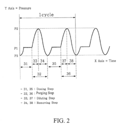
Atomic Layer Deposition (ALD) coating techniques are widely used in semiconductor manufacturing to create ultra-thin, conformal films with precise thickness control. These processes enable the deposition of high-quality barrier layers, dielectric materials, and conductive films for advanced microelectronic devices. The technology allows for atomic-level precision in coating complex 3D structures and high-aspect-ratio features, which is critical for next-generation semiconductor devices.- ALD coating processes for semiconductor applications: Atomic Layer Deposition (ALD) coating techniques are widely used in semiconductor manufacturing to create ultra-thin, conformal films with precise thickness control. These processes enable the deposition of high-quality barrier layers, dielectric materials, and conductive films for advanced microelectronic devices. The technology allows for atomic-level precision in coating complex 3D structures and high-aspect-ratio features, which is critical for next-generation semiconductor devices.
- ALD coating equipment and apparatus design: Specialized equipment and apparatus designs for Atomic Layer Deposition coating processes focus on optimizing precursor delivery, reaction chamber configuration, and substrate handling. These systems incorporate precise temperature control mechanisms, gas flow management, and vacuum technology to ensure uniform deposition across substrates. Innovations in ALD equipment design aim to improve throughput, reduce cycle times, and enable coating of larger or more complex substrates while maintaining the high-quality film characteristics inherent to ALD processes.
- ALD coating for energy storage and conversion devices: Atomic Layer Deposition coating technology is applied to energy storage and conversion devices such as batteries, fuel cells, and solar cells to enhance performance and durability. The ultra-thin, conformal coatings can protect electrode materials, improve interface properties, and create functional layers that enhance charge transfer or catalytic activity. These coatings help address challenges related to cycle life, efficiency, and stability in energy devices by providing precise control over surface chemistry and structure at the nanoscale.
- Novel materials and precursors for ALD coating: Development of novel materials and precursors for Atomic Layer Deposition enables the creation of coatings with enhanced properties and expanded functionality. Research focuses on precursor chemistry that allows deposition of complex oxides, nitrides, metals, and hybrid materials with specific electrical, optical, or mechanical characteristics. These innovations expand the application range of ALD technology and enable the creation of advanced functional coatings with precisely controlled composition, thickness, and structure.
- ALD coating for protective and barrier applications: Atomic Layer Deposition provides exceptional barrier and protective coatings for various substrates, including metals, polymers, and composites. These ultra-thin coatings offer protection against corrosion, oxidation, moisture, and chemical attack while maintaining the dimensional integrity of the underlying components. The conformal nature of ALD coatings ensures complete coverage of complex geometries and hard-to-reach surfaces, making them ideal for applications requiring high-performance environmental barriers with minimal thickness.
02 ALD coating for energy storage and conversion devices
ALD coating technology is applied to energy storage and conversion devices such as batteries, fuel cells, and solar cells to enhance performance and durability. The technique enables the deposition of protective layers, catalytic materials, and functional interfaces at the nanoscale. These coatings can improve electrode stability, prevent corrosion, enhance charge transfer, and extend the lifecycle of energy devices while maintaining their electrochemical performance.Expand Specific Solutions03 Equipment and apparatus for ALD coating processes
Specialized equipment and apparatus have been developed for implementing ALD coating processes across various industries. These systems include reaction chambers, gas delivery systems, temperature control mechanisms, and automation components designed to achieve precise layer-by-layer deposition. Advanced ALD equipment features innovations such as spatial ALD for higher throughput, multi-chamber configurations for complex coating sequences, and in-situ monitoring capabilities for quality control.Expand Specific Solutions04 ALD coating for corrosion and wear protection
ALD coatings provide exceptional corrosion and wear protection for various materials and components. The nanoscale protective layers created through ALD offer superior barrier properties against environmental degradation while maintaining the dimensional integrity of the coated parts. These coatings can be applied to complex geometries and internal surfaces that are difficult to reach with conventional coating methods, making them valuable for protecting critical components in harsh operating environments.Expand Specific Solutions05 Novel materials and precursors for ALD coating
Research and development in ALD coating technology has led to the creation of novel materials and precursors that expand the capabilities and applications of the process. These innovations include new metal-organic compounds, reactive gas combinations, and catalyst systems that enable the deposition of a wider range of materials with enhanced properties. Advanced precursor chemistry allows for lower deposition temperatures, faster reaction kinetics, and improved film quality in ALD processes.Expand Specific Solutions
Key ALD Patents for TFT Applications
Atomic layer deposition apparatus and atomic layer deposition method
PatentInactiveUS20100323125A1
Innovation
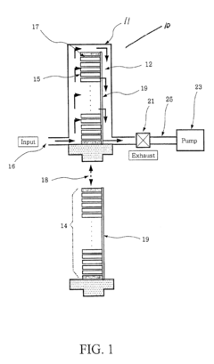
- The ALD apparatus separates the antenna array for plasma generation from the deposition chamber, using a connected auxiliary chamber to produce reactive gas radicals, which are then supplied to the deposition chamber, reducing particle generation and improving maintenance by avoiding complex configurations within the deposition container.
Method of forming a thin film using atomic layer deposition
PatentInactiveUS6828218B2
Innovation
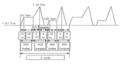
- A furnace-type ALD reactor with a single large-volume reaction space allows concurrent loading of multiple substrates and employs a method to dilute non-chemically adsorbed reactants, reducing purging time and increasing throughput by using an automatic wafer transfer mechanism.
Material Selection Strategies
Material selection is a critical factor in determining the performance and reliability of ALD (Atomic Layer Deposition) coatings in thin film transistor (TFT) production. The strategic approach to material selection must consider both the functional requirements of the TFT and the compatibility with the ALD process itself.
High-k dielectric materials have emerged as primary candidates for ALD coating in TFT applications, with aluminum oxide (Al2O3), hafnium oxide (HfO2), and zirconium oxide (ZrO2) demonstrating superior electrical properties. These materials offer excellent dielectric constants ranging from 9 for Al2O3 to approximately 25 for HfO2, enabling reduced leakage current while maintaining high capacitance in thin film structures.
The selection process must account for the interface quality between the semiconductor channel and the dielectric layer. Materials that form clean interfaces with minimal defect states are preferred, as interface traps significantly impact carrier mobility and threshold voltage stability. Silicon dioxide (SiO2) remains valuable as an interfacial layer due to its exceptional interface properties with silicon-based semiconductors, though it is often combined with high-k materials in a multilayer approach.
Thermal budget considerations play a crucial role in material selection, particularly for flexible electronics applications. Materials that can be deposited at lower temperatures (<200°C) without sacrificing film quality are increasingly important. Zinc oxide (ZnO) and titanium oxide (TiO2) have shown promise in this regard, enabling ALD processes compatible with temperature-sensitive substrates like polyethylene terephthalate (PET) or polyimide.
Precursor chemistry represents another vital aspect of material selection strategy. The ideal precursors should exhibit high volatility, thermal stability, and complete reactions with surface sites. Metal-organic compounds such as trimethylaluminum (TMA) for aluminum oxide and tetrakis(dimethylamido)hafnium (TDMAH) for hafnium oxide have become industry standards due to their favorable reaction kinetics and minimal impurity incorporation.
Emerging materials including ternary compounds (e.g., HfSiOx, AlTiOx) and doped oxides are gaining attention for their ability to fine-tune electrical properties. These engineered materials allow for precise control over band alignment, dielectric constant, and leakage current characteristics, enabling optimization for specific TFT applications ranging from high-performance computing to low-power flexible displays.
The long-term stability of selected materials must also be evaluated, particularly regarding resistance to moisture penetration and chemical degradation. Encapsulation strategies often incorporate multilayer approaches where materials are selected not only for their electrical properties but also for their barrier characteristics against environmental contaminants.
Scaling Considerations for Mass Production
Scaling ALD coating processes for mass production of thin film transistors (TFTs) presents several critical challenges that must be addressed to achieve commercial viability. The transition from laboratory-scale to industrial-scale production requires significant engineering adaptations to maintain the exceptional quality of ALD films while increasing throughput and reducing costs.
Throughput optimization represents the primary challenge in scaling ALD processes. Traditional ALD techniques operate in cycles that typically require 1-10 seconds per monolayer, resulting in extremely slow deposition rates compared to other thin film deposition methods. For mass production environments, spatial ALD configurations have emerged as promising solutions, enabling continuous rather than sequential processing. These systems can achieve deposition rates 10-100 times faster than conventional ALD while maintaining excellent film quality.
Equipment design considerations are equally important for industrial implementation. Roll-to-roll ALD systems have demonstrated particular promise for high-volume TFT production, especially for flexible electronics applications. These systems allow continuous processing of substrate materials through reaction zones, significantly enhancing production efficiency. Additionally, multi-wafer batch processing systems have been developed for silicon-based TFTs, enabling simultaneous coating of multiple substrates.
Cost factors must be carefully evaluated when scaling ALD processes. While ALD offers superior film quality and thickness control, the associated equipment costs and relatively slow processing speeds have historically limited widespread industrial adoption. Recent advancements in precursor chemistry have reduced material costs, and improved reactor designs have enhanced precursor utilization efficiency, making ALD increasingly economically viable for TFT production.
Quality control systems require sophisticated adaptation for high-volume manufacturing environments. In-line metrology tools capable of real-time film thickness and uniformity measurements are essential for maintaining process control. Advanced process control algorithms that can make real-time adjustments to maintain film quality across large substrate areas have been developed specifically for industrial ALD systems.
Integration with existing semiconductor manufacturing lines presents another scaling consideration. ALD equipment must be compatible with standard clean room environments and automation systems. Cluster tool configurations that combine ALD with other process steps (etching, annealing, etc.) have proven effective at minimizing handling and contamination risks while maximizing production efficiency.
Environmental and safety considerations also become more prominent at industrial scales. Precursor recovery systems and abatement technologies must be implemented to minimize waste and emissions. Water and energy consumption optimization becomes increasingly important as production volumes grow, driving development of more efficient heating and cooling systems for ALD reactors.
Unlock deeper insights with Patsnap Eureka Quick Research — get a full tech report to explore trends and direct your research. Try now!
Generate Your Research Report Instantly with AI Agent
Supercharge your innovation with Patsnap Eureka AI Agent Platform!