The Impact of ALD Coating on Dielectric Breakdown Strength
SEP 25, 202510 MIN READ
Generate Your Research Report Instantly with AI Agent
Patsnap Eureka helps you evaluate technical feasibility & market potential.
ALD Coating Technology Background and Objectives
Atomic Layer Deposition (ALD) technology has evolved significantly since its inception in the 1970s, transitioning from a laboratory curiosity to a critical manufacturing process in semiconductor fabrication. The technique's unique ability to deposit uniform, conformal thin films with precise thickness control at the atomic scale has positioned it as an essential technology across multiple industries. Initially developed for microelectronics applications, ALD has expanded its utility into energy storage, catalysis, and protective coatings, demonstrating remarkable versatility in addressing various material engineering challenges.
The evolution of ALD technology has been characterized by continuous improvements in precursor chemistry, reactor design, and process control systems. Early implementations were limited by slow deposition rates and a narrow range of compatible materials. However, recent advancements have dramatically expanded the portfolio of ALD-compatible materials to include oxides, nitrides, metals, and hybrid organic-inorganic compounds, significantly broadening its application potential.
In the context of dielectric breakdown strength enhancement, ALD coating represents a promising frontier. Dielectric breakdown—the catastrophic failure of an insulating material under electric field stress—remains a critical limitation in high-voltage applications, energy storage systems, and advanced electronics. Traditional approaches to improving breakdown strength have focused on material purity and processing conditions, but these methods are approaching their theoretical limits.
ALD technology offers a paradigm shift in addressing this challenge through the deposition of ultra-thin, defect-free barrier layers that can significantly enhance dielectric properties. The atomic-level control inherent to ALD enables the creation of engineered interfaces and nanolaminate structures that can effectively suppress electron avalanche processes—the primary mechanism behind dielectric breakdown.
The primary technical objectives in this domain include developing ALD processes capable of depositing high-quality dielectric films with superior breakdown strength, understanding the fundamental mechanisms by which ALD coatings enhance dielectric performance, and scaling these processes for industrial implementation. Additionally, there is significant interest in exploring novel material combinations and multilayer architectures that can push dielectric breakdown strength beyond current limitations.
Current research trends indicate a growing focus on high-k dielectric materials deposited via ALD for next-generation power electronics, electric vehicles, and renewable energy systems. The ability to precisely engineer interfaces at the nanoscale presents unprecedented opportunities for creating dielectric systems with exceptional performance characteristics, potentially enabling transformative advances in energy density, operational lifetime, and system reliability.
Market Demand Analysis for Enhanced Dielectric Materials
The global market for enhanced dielectric materials is experiencing significant growth, driven by the increasing demand for high-performance electronic components across multiple industries. The integration of Atomic Layer Deposition (ALD) coating technology to improve dielectric breakdown strength represents a critical advancement addressing these market needs. Current market analysis indicates that the power electronics sector alone is projected to reach $25 billion by 2025, with dielectric materials constituting a substantial segment of this market.
Industries such as renewable energy, electric vehicles, and advanced computing are primary drivers of demand for enhanced dielectric materials. The electric vehicle market, growing at approximately 24% annually, requires capacitors and insulators with superior breakdown strength to support high-voltage power systems. Similarly, the renewable energy sector's expansion necessitates more reliable power conversion equipment capable of handling higher voltages and operating in harsh environmental conditions.
Data center infrastructure represents another significant market segment, with global spending on data center systems reaching $208 billion in 2020. The demand for more efficient power distribution and management systems within these facilities creates substantial opportunities for ALD-coated dielectric materials that can withstand higher voltages while maintaining compact form factors.
Consumer electronics manufacturers are increasingly seeking miniaturized components with enhanced reliability, creating demand for dielectric materials with improved breakdown strength. This trend is particularly evident in smartphones, wearables, and IoT devices where space constraints are significant but performance expectations remain high.
Market research indicates that companies investing in enhanced dielectric materials can achieve competitive advantages through improved product reliability, extended service life, and reduced maintenance costs. End-users report willingness to pay premium prices for components with demonstrably superior dielectric properties, particularly in mission-critical applications where failure is not an option.
Regional analysis shows North America and Asia-Pacific leading market demand, with Europe following closely due to stringent energy efficiency regulations driving adoption of advanced power electronics. China's aggressive investment in electric vehicle infrastructure and renewable energy has created a particularly strong growth market for enhanced dielectric materials in the Asia-Pacific region.
Industry surveys reveal that manufacturers prioritize three key performance metrics when selecting dielectric materials: breakdown strength, temperature stability, and long-term reliability. ALD coating technology directly addresses these priorities by providing nanoscale precision in material deposition that significantly enhances dielectric breakdown strength while maintaining other critical performance parameters.
Current Status and Challenges in ALD Dielectric Coatings
Atomic Layer Deposition (ALD) has emerged as a pivotal technology for creating high-quality dielectric coatings with exceptional precision and conformality. Currently, ALD dielectric coatings are being extensively researched and implemented across various industries, particularly in semiconductor manufacturing, energy storage systems, and advanced electronics. The state-of-the-art ALD processes can achieve atomic-level control over film thickness and composition, enabling the creation of ultra-thin dielectric layers with superior breakdown strength characteristics.
Globally, research institutions and industry leaders have made significant advancements in ALD technology. North America and East Asia dominate the research landscape, with Europe also contributing substantially to innovation in this field. The geographical distribution of ALD expertise reflects the concentration of semiconductor and electronics manufacturing facilities, with notable research clusters in the United States, South Korea, Japan, and Taiwan.
Despite impressive progress, several critical challenges persist in ALD dielectric coating technology. One fundamental limitation is the relatively slow deposition rate, which impacts manufacturing throughput and economic viability for large-scale production. Typical ALD processes operate at rates of 0.1-1.0 nm per minute, significantly slower than alternative deposition methods. This speed constraint remains a major hurdle for broader industrial adoption.
Another significant challenge involves the complex relationship between processing parameters and dielectric breakdown strength. Researchers continue to grapple with optimizing temperature, precursor chemistry, and cycle timing to maximize breakdown strength while maintaining other desirable properties. The interdependence of these parameters creates a multidimensional optimization problem that requires sophisticated modeling and experimental approaches.
Material interface quality presents another persistent challenge. The breakdown strength of ALD dielectric coatings is heavily influenced by the quality of interfaces between the substrate and the coating, as well as between different layers in multi-layer structures. Controlling interfacial defects, preventing diffusion, and managing stress at these boundaries remain technically demanding.
Scalability issues also constrain wider implementation. While ALD excels in coating complex 3D structures with high aspect ratios, achieving uniform coating quality across large substrate areas or in high-volume manufacturing environments presents significant engineering challenges. Batch processing limitations and equipment design constraints further complicate industrial scaling efforts.
Environmental considerations pose additional challenges, as some traditional ALD precursors have high global warming potential or present safety hazards. The industry is actively seeking more environmentally benign alternatives that maintain or improve dielectric performance while reducing environmental impact.
Current Technical Solutions for Dielectric Breakdown Prevention
01 ALD coating materials for enhanced dielectric breakdown strength
Various materials deposited via Atomic Layer Deposition (ALD) can significantly improve dielectric breakdown strength. High-k materials such as aluminum oxide (Al2O3), hafnium oxide (HfO2), and zirconium oxide (ZrO2) are particularly effective due to their superior insulating properties. These materials can be precisely deposited in ultra-thin, conformal layers with excellent uniformity, which is critical for maintaining high breakdown strength across the entire coated surface.- ALD coating materials for enhanced dielectric breakdown strength: Various materials deposited via Atomic Layer Deposition (ALD) can significantly enhance dielectric breakdown strength. High-k dielectric materials such as aluminum oxide, hafnium oxide, and zirconium oxide are particularly effective. These materials create uniform, pinhole-free thin films that maintain excellent insulating properties even at reduced thicknesses, resulting in improved breakdown voltage performance for electronic components and capacitors.
- Multi-layer ALD structures for improved breakdown strength: Multilayer ALD structures consisting of alternating layers of different dielectric materials can significantly improve breakdown strength. These nanolaminate structures distribute the electric field more evenly and block defect propagation pathways. The interfaces between different materials act as barriers to electron movement, effectively increasing the overall breakdown voltage. This approach allows for customized dielectric properties by combining materials with complementary characteristics.
- Process parameters optimization for ALD dielectric coatings: Optimizing ALD process parameters is crucial for maximizing dielectric breakdown strength. Key parameters include deposition temperature, precursor pulse duration, purge time, and number of cycles. Lower deposition temperatures often result in denser films with fewer defects, while proper purge times prevent unwanted reactions that could introduce impurities. Post-deposition annealing in specific atmospheres can further enhance dielectric properties by reducing defects and improving film crystallinity.
- ALD coatings for power electronic applications: ALD coatings provide superior dielectric breakdown strength for power electronic applications such as capacitors, transistors, and integrated circuits. These thin film coatings enable miniaturization while maintaining or improving electrical performance. The precise thickness control and conformality of ALD make it particularly valuable for high-voltage applications where reliability is critical. The enhanced breakdown strength allows for operation at higher voltages or with thinner insulating layers, improving energy density in storage devices.
- Doping and interface engineering for ALD dielectric films: Doping ALD dielectric films with specific elements and engineering interfaces can significantly enhance breakdown strength. Introducing dopants like nitrogen, silicon, or rare earth elements can modify the band structure and trap density in the dielectric. Interface engineering techniques such as plasma treatment or insertion of buffer layers reduce interface states and charge trapping. These approaches minimize leakage current and electron injection, resulting in higher breakdown fields and improved reliability under electrical stress.
02 Multi-layer ALD structures for improved breakdown performance
Multilayered ALD structures consisting of alternating dielectric materials can significantly enhance breakdown strength compared to single-layer coatings. These nanolaminate structures distribute the electric field more effectively and provide multiple barriers against leakage current. The interfaces between different materials can act as traps for charge carriers, preventing them from gaining enough energy to cause dielectric breakdown. Optimizing the thickness ratio between layers is crucial for maximizing the overall breakdown strength.Expand Specific Solutions03 Process parameters affecting ALD coating breakdown strength
Critical ALD process parameters significantly impact the dielectric breakdown strength of the resulting coatings. These include deposition temperature, precursor pulse duration, purge time, and number of cycles. Lower deposition temperatures often result in fewer defects and impurities, while adequate purge times prevent unwanted CVD-like reactions that can introduce weaknesses. Post-deposition annealing in controlled atmospheres can further enhance breakdown strength by reducing defects and improving film crystallinity.Expand Specific Solutions04 Defect engineering in ALD dielectric films
Controlling and minimizing defects in ALD dielectric films is essential for maximizing breakdown strength. Techniques include precise control of oxygen vacancies, incorporation of dopants to passivate defect sites, and interface engineering to reduce trap states. Hydrogen or nitrogen incorporation during or after deposition can passivate dangling bonds that would otherwise act as weak points for electrical breakdown. Advanced characterization techniques such as conductive atomic force microscopy can identify nanoscale defects that affect breakdown performance.Expand Specific Solutions05 Applications of high-breakdown ALD coatings in electronic devices
ALD coatings with enhanced dielectric breakdown strength enable significant advancements in various electronic applications. In capacitors, these coatings allow for higher energy storage density and improved reliability under high electric fields. For semiconductor devices, they enable thinner gate dielectrics with reduced leakage current, supporting continued device scaling. In power electronics, high-breakdown ALD films provide superior insulation for high-voltage operation. These coatings are also finding applications in emerging technologies such as flexible electronics and energy storage devices where conventional insulation methods are inadequate.Expand Specific Solutions
Key Industry Players in ALD Coating Development
The ALD coating technology for enhancing dielectric breakdown strength is currently in a growth phase, with the market expanding rapidly due to increasing demand for high-performance electronic components. The global market size is estimated to reach several billion dollars by 2025, driven by applications in semiconductor manufacturing and energy storage. Technologically, industry leaders like Taiwan Semiconductor Manufacturing Co., Applied Materials, and Forge Nano have achieved significant maturity in ALD implementation, with companies such as Micron Technology and Samsung Electronics integrating these solutions into their advanced manufacturing processes. Emerging players like ALD NanoSolutions and SilcoTek are advancing specialized coating technologies, while research collaboration between established semiconductor manufacturers and equipment providers is accelerating innovation in dielectric performance enhancement.
Forge Nano, Inc.
Technical Solution: Forge Nano has developed a proprietary Atomic Armor™ technology platform that utilizes advanced ALD coating processes specifically optimized for enhancing dielectric breakdown strength. Their approach focuses on ultra-thin protective coatings (typically 2-20nm) that can be applied to various substrate materials including ceramics, polymers, and metal oxides used in energy storage and power electronics applications. Forge Nano's technology enables precise control over coating composition and thickness, creating defect-free barrier layers that significantly improve dielectric performance. Their proprietary spatial ALD process allows for high-throughput manufacturing while maintaining the quality benefits of traditional ALD. Independent testing has demonstrated that their ALD coatings can increase dielectric breakdown strength by 30-70% depending on the substrate material, while also improving long-term reliability under electrical stress conditions. The company has successfully implemented these coatings in commercial applications including lithium-ion battery components and high-voltage capacitors.
Strengths: Specialized expertise in high-volume ALD manufacturing; demonstrated commercial implementation across multiple industries; ability to coat complex geometries and porous materials with uniform layers. Weaknesses: More focused on energy storage applications than traditional semiconductor manufacturing; relatively newer entrant compared to established semiconductor equipment manufacturers; limited public data on long-term performance in extreme environments.
Applied Materials, Inc.
Technical Solution: Applied Materials has developed advanced ALD coating solutions specifically designed to enhance dielectric breakdown strength in semiconductor devices. Their Endura® platform incorporates precision ALD technology that enables conformal deposition of high-k dielectric materials with atomic-level thickness control. The company's ALD process creates ultra-thin, pinhole-free barrier layers that significantly improve dielectric breakdown strength by minimizing defect density and providing uniform coverage even in high-aspect-ratio structures. Their proprietary Sequential Flow™ ALD technology allows for precise interface engineering between the dielectric and electrode materials, which has been shown to increase breakdown field strength by up to 40% compared to conventional deposition methods. Applied Materials has also pioneered plasma-enhanced ALD (PEALD) techniques that enable lower temperature processing while maintaining excellent film quality, critical for temperature-sensitive applications requiring high dielectric strength.
Strengths: Industry-leading precision in layer thickness control (±0.1Å); excellent conformality even in complex 3D structures; high throughput capability for manufacturing environments. Weaknesses: Higher implementation cost compared to conventional deposition methods; requires specialized expertise for process optimization; some processes may need higher temperatures that limit compatibility with certain materials.
Critical Patents and Research on ALD Dielectric Enhancement
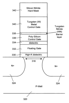
Dielectric layer created using ALD to deposit multiple components
PatentInactiveUS20060027882A1
Innovation
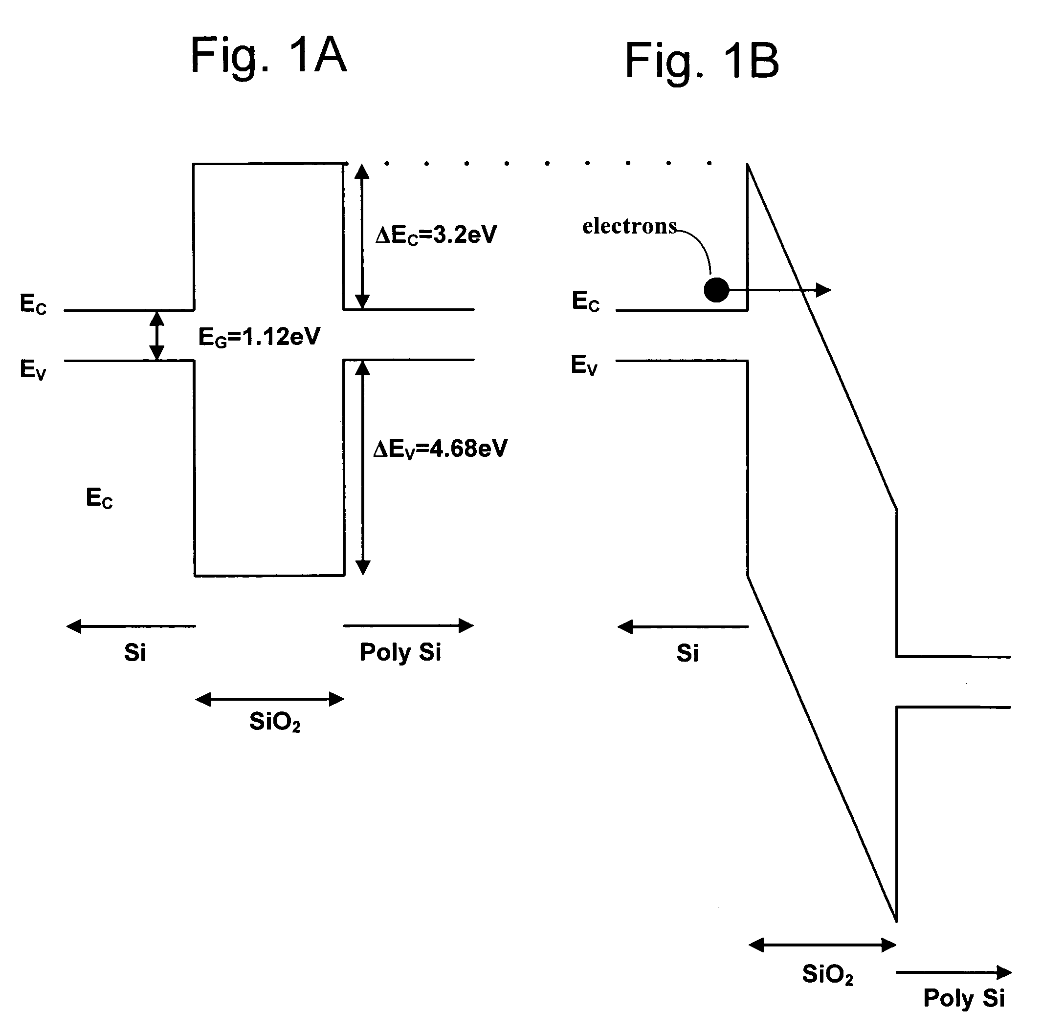
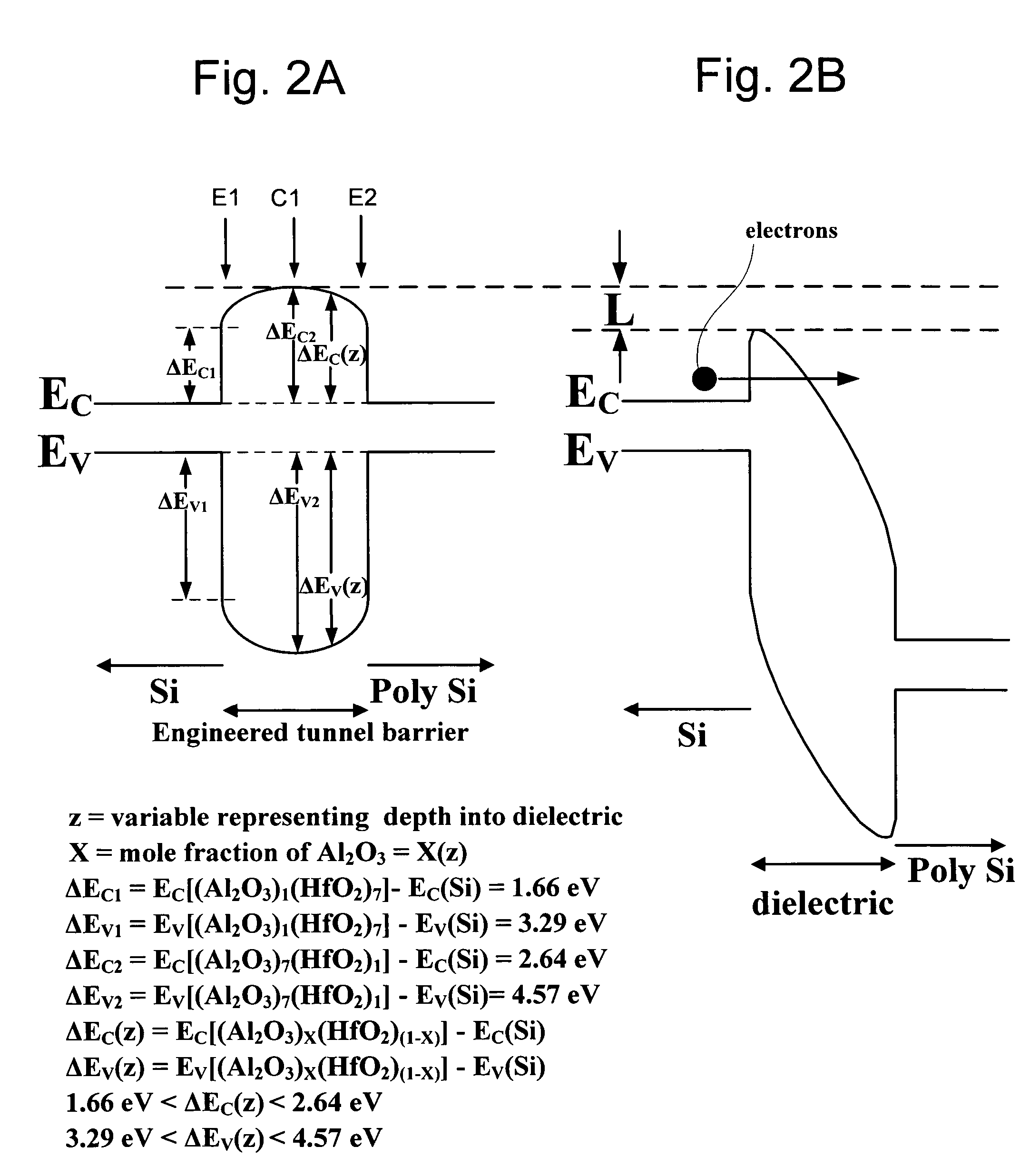
- A dielectric layer with a rounded bottom conduction band profile is created using atomic layer deposition, comprising multiple components with varying mole fractions, to facilitate efficient charge injection and reduce the voltage required for programming and erasing, achieved by gradually transitioning between different dielectric materials to optimize the conduction band profile.
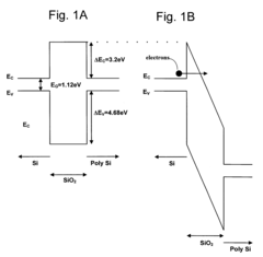
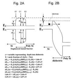
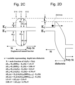
Creating a dielectric layer using ALD to deposit multiple components
PatentInactiveUS20060008999A1
Innovation
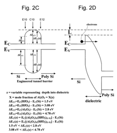
- A dielectric layer with a rounded bottom of the conduction band profile is created using atomic layer deposition (ALD) by varying the mole fractions of components like HfO2 and Al2O3 as a function of depth, reducing the barrier height and facilitating faster charge injection through crested tunnel barriers.
Material Compatibility and Interface Engineering Considerations
Material compatibility represents a critical factor in the successful implementation of ALD coating technologies for enhancing dielectric breakdown strength. When depositing thin films onto substrate materials, the chemical and physical interactions at the interface significantly influence the overall performance of the dielectric system. Different substrate materials exhibit varying degrees of compatibility with ALD precursors, potentially leading to issues such as poor adhesion, interfacial defects, or unwanted chemical reactions that compromise the intended enhancement of breakdown strength.
The interface between the ALD coating and the substrate requires careful engineering to minimize defects and ensure optimal performance. Surface preparation techniques, including cleaning protocols and activation methods, play a vital role in creating favorable conditions for uniform film growth. Research indicates that hydroxyl-terminated surfaces often provide ideal anchoring sites for initial ALD reactions, promoting strong chemical bonding between the coating and substrate. Plasma treatment and chemical functionalization have emerged as effective approaches to modify surface properties and improve compatibility.
Thermal expansion coefficient mismatches between the substrate and ALD coating materials present significant challenges, particularly in applications involving temperature fluctuations. These mismatches can induce mechanical stress at the interface, potentially leading to delamination or crack formation that creates pathways for electrical breakdown. Selection of materials with compatible thermal properties or the implementation of buffer layers can mitigate these effects, preserving the integrity of the dielectric system under varying operational conditions.
Interfacial charge trapping represents another critical consideration in ALD coating applications for dielectric systems. The interface between dissimilar materials often contains structural defects and dangling bonds that can trap charges, potentially reducing the effective breakdown strength. Advanced interface engineering techniques, such as the deposition of ultra-thin transition layers or controlled doping of the interfacial region, can neutralize these trap sites and create more electrically robust boundaries.
Chemical diffusion across the interface during both the deposition process and subsequent operation can compromise the distinct properties of each material layer. Elements from the substrate may migrate into the ALD coating, or vice versa, altering the intended composition and potentially introducing electrically active defects. Diffusion barrier layers and optimized deposition parameters can help maintain the chemical integrity of the interface, preserving the enhanced dielectric properties provided by the ALD coating.
Recent advances in in-situ characterization techniques have significantly improved our understanding of interface formation during ALD processes. Techniques such as quartz crystal microbalance, spectroscopic ellipsometry, and synchrotron-based X-ray methods now enable real-time monitoring of interface development, allowing for more precise control over the critical early stages of film growth that determine long-term dielectric performance.
Scalability and Cost Analysis of ALD Implementation
The implementation of Atomic Layer Deposition (ALD) coating technology for enhancing dielectric breakdown strength presents significant scalability challenges and cost considerations that must be carefully evaluated. Current industrial ALD systems demonstrate varying throughput capabilities, ranging from 10-100 wafers per hour for semiconductor applications to considerably lower rates for complex three-dimensional structures requiring conformal coatings. This throughput limitation represents a primary scalability constraint when considering widespread adoption across various industries.
Capital expenditure for industrial-scale ALD equipment typically ranges from $500,000 to several million dollars, depending on chamber size, automation level, and process capabilities. Additionally, operational costs include high-purity precursor materials, which can cost $500-2,000 per kilogram, and significant energy consumption for maintaining vacuum conditions and precise temperature control during deposition cycles.
The economic viability of ALD implementation varies substantially across application sectors. In high-value electronics where performance improvements directly translate to competitive advantages, the cost-benefit ratio often justifies implementation despite high initial investments. Conversely, in large-scale applications like power transmission infrastructure, the economics become more challenging unless significant performance enhancements can be demonstrated.
Recent technological advancements are gradually improving the cost-effectiveness of ALD processes. Spatial ALD techniques have emerged as promising alternatives to traditional temporal ALD, potentially increasing throughput by 10-100 times while maintaining coating quality. Additionally, roll-to-roll ALD systems for flexible substrates are showing promise for continuous processing applications, potentially reducing per-unit costs for certain applications.
Material efficiency improvements represent another avenue for cost reduction. Research indicates that precursor utilization rates in conventional ALD systems often fall below 30%, presenting significant opportunities for optimization. Advanced precursor delivery systems and recovery mechanisms could potentially reduce material costs by 40-60% while simultaneously addressing environmental concerns related to waste.
For organizations considering ALD implementation, a phased approach often proves most economically viable. Beginning with critical components where dielectric performance improvements deliver the highest value allows for validation of performance benefits before broader implementation. This strategy enables more accurate cost-benefit analysis based on application-specific performance data rather than theoretical projections.
Unlock deeper insights with Patsnap Eureka Quick Research — get a full tech report to explore trends and direct your research. Try now!
Generate Your Research Report Instantly with AI Agent
Supercharge your innovation with Patsnap Eureka AI Agent Platform!