Exploring Regulatory Hurdles in ALD Coating for High-Tech Manufacturing
SEP 25, 20259 MIN READ
Generate Your Research Report Instantly with AI Agent
Patsnap Eureka helps you evaluate technical feasibility & market potential.
ALD Coating Technology Background and Objectives
Atomic Layer Deposition (ALD) technology has evolved significantly since its inception in the 1970s, transitioning from a laboratory curiosity to a critical manufacturing process in high-tech industries. Originally developed for semiconductor fabrication, ALD has expanded its application scope to include microelectronics, energy storage, medical devices, and aerospace components. The technology's unique ability to deposit uniform, conformal thin films with atomic-level precision has positioned it as an indispensable tool in modern manufacturing processes requiring nanoscale precision.
The evolution of ALD technology has been marked by several key milestones, including the development of thermal ALD processes in the 1980s, plasma-enhanced ALD in the 1990s, and spatial ALD in the 2000s. Each advancement has expanded the range of materials that can be deposited and improved process efficiency. Recent innovations have focused on low-temperature ALD processes, enabling coating of temperature-sensitive substrates and expanding applications into flexible electronics and biomedical devices.
Current technological trends in ALD coating include the development of area-selective deposition techniques, integration with other manufacturing processes, and scaling for high-volume production. The industry is witnessing a shift toward more environmentally friendly precursors and processes, driven by increasing regulatory scrutiny of traditional chemicals used in ALD processes.
The primary objective of exploring regulatory hurdles in ALD coating is to identify and address compliance challenges that may impede the technology's broader adoption across high-tech manufacturing sectors. This includes understanding the complex landscape of chemical regulations, workplace safety requirements, environmental protection standards, and product-specific certifications that vary significantly across global markets.
Secondary objectives include developing strategies for navigating regulatory frameworks efficiently, anticipating future regulatory changes, and establishing best practices for compliance that balance innovation with regulatory requirements. This exploration aims to provide a roadmap for manufacturers to implement ALD technology while minimizing regulatory risks and delays.
The long-term goal is to facilitate the integration of ALD coating into mainstream manufacturing processes by removing regulatory barriers, thereby enabling industries to fully leverage the technology's advantages in creating next-generation products with enhanced performance characteristics. This includes establishing industry standards and protocols that can streamline regulatory approval processes while ensuring safety and environmental protection.
Understanding these regulatory challenges is particularly crucial as ALD technology expands beyond traditional semiconductor applications into consumer electronics, medical devices, and other highly regulated industries where compliance requirements are more stringent and complex.
Market Demand Analysis for ALD Coating Solutions
The global market for Atomic Layer Deposition (ALD) coating solutions has experienced significant growth in recent years, driven primarily by the increasing demand for miniaturization in semiconductor devices and the expanding applications in various high-tech manufacturing sectors. The current market size for ALD equipment and services is estimated to reach $3.7 billion by 2025, with a compound annual growth rate of approximately 22% from 2020 to 2025.
The semiconductor industry remains the largest consumer of ALD technology, accounting for nearly 65% of the total market share. This dominance is attributed to the critical role ALD plays in enabling the continued scaling of integrated circuits according to Moore's Law. As transistor dimensions shrink below 5nm, conventional deposition techniques become inadequate, making ALD the preferred method for depositing ultra-thin, conformal films with atomic-level precision.
Beyond semiconductors, there is growing adoption of ALD in emerging applications such as medical devices, renewable energy technologies, and aerospace components. The medical device sector, in particular, has shown increased interest in ALD coatings for implantable devices due to their biocompatibility and corrosion resistance properties. Market analysis indicates this segment is growing at 27% annually, outpacing the overall ALD market growth.
Geographically, Asia-Pacific dominates the ALD market with approximately 58% share, primarily due to the concentration of semiconductor manufacturing in countries like Taiwan, South Korea, and China. North America follows with 22% market share, driven by advanced research and development activities in both academic and industrial settings.
A significant market trend is the increasing demand for batch ALD systems that offer higher throughput while maintaining coating quality. This trend reflects manufacturers' focus on improving production efficiency to meet growing volume requirements while managing costs. The batch ALD segment is projected to grow at 25% annually through 2025.
Regulatory considerations are becoming increasingly important market drivers. As environmental regulations tighten globally, manufacturers are seeking ALD solutions that use less hazardous precursors and reduce waste. This regulatory pressure is creating new market opportunities for environmentally friendly ALD technologies and processes.
Customer requirements are also evolving, with greater emphasis on flexibility in ALD systems that can handle multiple substrate materials and geometries. This trend is particularly evident in emerging applications like flexible electronics and energy storage devices, where coating requirements vary significantly from traditional semiconductor applications.
Global ALD Technology Landscape and Challenges
Atomic Layer Deposition (ALD) technology has evolved significantly over the past three decades, transforming from a niche research technique to a critical manufacturing process in high-tech industries. The global landscape of ALD technology presents a complex picture of rapid advancement coupled with persistent technical and regulatory challenges. Currently, ALD is widely adopted in semiconductor manufacturing, where it enables the production of increasingly miniaturized and complex microelectronic components with atomic-level precision.
The geographical distribution of ALD technology development shows concentration in several key regions. North America, particularly the United States, leads in research innovation and patent filings, with major semiconductor companies and research institutions driving advancements. East Asia, including South Korea, Japan, Taiwan, and increasingly China, dominates in terms of implementation scale, with massive semiconductor fabrication facilities utilizing ALD processes. Europe maintains strength in equipment manufacturing and specialized applications, particularly in Finland, Germany, and the Netherlands.
Despite widespread adoption, ALD technology faces significant challenges globally. Technical hurdles include achieving uniform deposition on complex 3D structures, optimizing precursor chemistry for new materials, and scaling processes for larger substrates while maintaining atomic-level precision. The industry also struggles with throughput limitations that impact production economics, particularly for high-volume manufacturing applications outside the semiconductor sector.
Regulatory frameworks present another layer of complexity in the global ALD landscape. Environmental regulations concerning precursor chemicals vary significantly across regions, creating compliance challenges for multinational operations. In the European Union, REACH regulations impose strict requirements on chemical usage, while the United States EPA and Asian regulatory bodies maintain different standards and reporting requirements. These regulatory disparities create barriers to technology transfer and global implementation.
The competitive landscape reveals an industry dominated by a few major equipment manufacturers, including Applied Materials, ASM International, and Picosun, alongside numerous specialized players focusing on specific applications or materials. This concentration has implications for technology access and pricing, particularly for emerging markets and applications.
Recent technological trends show increasing focus on spatial ALD for higher throughput, low-temperature processes for temperature-sensitive substrates, and integration of in-situ monitoring for process optimization. Additionally, research into new precursors and plasma-enhanced processes is expanding the range of materials that can be deposited using ALD techniques, opening new application possibilities in areas such as energy storage, medical devices, and quantum computing.
Current ALD Coating Implementation Strategies
01 Regulatory compliance for ALD coatings in medical devices
Atomic Layer Deposition (ALD) coatings used in medical devices face specific regulatory hurdles related to biocompatibility, safety, and efficacy. Manufacturers must demonstrate that these coatings meet stringent requirements for patient safety, including testing for potential leaching of materials, durability under physiological conditions, and compatibility with sterilization processes. Regulatory bodies require extensive documentation on the coating process parameters, quality control measures, and validation studies before approval.- Regulatory compliance for ALD coatings in medical devices: Atomic Layer Deposition (ALD) coatings used in medical devices face significant regulatory hurdles, particularly regarding biocompatibility and safety standards. Manufacturers must demonstrate that these coatings meet specific requirements for medical applications, including non-toxicity, durability, and compatibility with biological tissues. The regulatory process involves extensive testing and documentation to ensure that the coated devices comply with healthcare regulations before market approval.
- Environmental regulations for ALD coating processes: ALD coating processes must comply with environmental regulations concerning emissions, waste management, and chemical handling. These regulations vary by jurisdiction but typically address the use of precursor chemicals, some of which may be hazardous or have environmental impacts. Manufacturers need to implement proper containment systems, waste treatment processes, and monitoring protocols to ensure compliance with air quality standards and chemical safety regulations.
- Quality control standards for industrial ALD applications: Industrial applications of ALD coatings are subject to strict quality control standards that present regulatory challenges. These standards govern coating thickness uniformity, adhesion strength, and performance characteristics. Manufacturers must implement robust quality management systems, including in-process monitoring, testing protocols, and documentation procedures to demonstrate compliance with industry-specific standards and specifications for their coated products.
- Intellectual property considerations in ALD technology: The ALD coating field involves complex intellectual property considerations that create regulatory hurdles for implementation. Companies must navigate patent landscapes, licensing requirements, and potential infringement issues when developing or applying ALD technologies. This includes conducting freedom-to-operate analyses and securing appropriate licenses or developing alternative approaches to avoid patent conflicts, which can significantly impact the commercialization timeline and costs.
- International trade and export control regulations: ALD coating technologies, particularly those with dual-use applications, face regulatory hurdles related to international trade and export controls. These regulations restrict the transfer of certain advanced coating technologies across borders due to national security concerns. Companies must comply with export licensing requirements, end-user verification processes, and technology transfer restrictions, which vary by country and can significantly impact global business operations and supply chains.
02 Environmental and safety regulations for ALD processes
ALD coating processes often involve the use of precursor chemicals that may be subject to environmental and workplace safety regulations. These include restrictions on volatile organic compounds (VOCs), hazardous air pollutants, and chemical handling procedures. Manufacturers implementing ALD technology must address waste management, emissions control, and worker exposure limits. Compliance with regulations such as REACH in Europe, EPA guidelines in the US, and similar frameworks in other regions presents significant hurdles for industrial adoption of ALD coating technologies.Expand Specific Solutions03 Quality control and standardization challenges
The lack of universally accepted standards specifically for ALD coating processes creates regulatory challenges. Manufacturers must develop and validate their own quality control protocols to ensure coating uniformity, adhesion, and performance characteristics. This includes establishing appropriate testing methodologies, acceptance criteria, and process monitoring techniques. The absence of standardized approaches increases the regulatory burden as each implementation requires individual justification and validation to satisfy regulatory requirements across different jurisdictions.Expand Specific Solutions04 Intellectual property and patent compliance
ALD coating technologies are subject to a complex landscape of patents and intellectual property rights that create regulatory hurdles for implementation. Companies must navigate existing patents to avoid infringement while developing their coating processes. This often requires extensive freedom-to-operate analyses, licensing agreements, or development of alternative approaches. The intellectual property considerations can significantly impact the regulatory pathway, particularly for novel applications of ALD coatings in regulated industries.Expand Specific Solutions05 Industry-specific certification requirements
Different industries impose specific certification requirements for ALD coatings based on their application. For example, coatings used in semiconductor manufacturing face different regulatory hurdles than those used in automotive or aerospace applications. These industry-specific requirements may include performance testing under extreme conditions, compatibility with other materials, durability standards, and specialized documentation. Manufacturers must adapt their regulatory strategies to address the particular certification frameworks relevant to their target markets.Expand Specific Solutions
Key Industry Players and Competitive Analysis
The ALD coating technology market for high-tech manufacturing is currently in a growth phase, characterized by increasing adoption across semiconductor, electronics, and advanced materials sectors. The global market size is expanding rapidly, projected to reach several billion dollars by 2025, driven by demands for precise nanoscale coatings. From a technical maturity perspective, the landscape shows varied development levels among key players. Industry leaders like Applied Materials, ASM International, and Lam Research have established robust ALD capabilities for semiconductor applications, while companies such as Picosun, Beneq, and Forge Nano are advancing specialized applications. Regulatory challenges remain significant, particularly regarding chemical precursor handling, environmental compliance, and integration with existing manufacturing processes, creating both barriers to entry and competitive advantages for established players with regulatory expertise.
ASM INTERNATIONAL NV
Technical Solution: ASM International has developed comprehensive regulatory compliance frameworks specifically for ALD processes in semiconductor manufacturing. Their approach includes advanced precursor delivery systems that minimize hazardous material usage while maintaining deposition quality. The company has pioneered environmentally-friendly ALD precursors that comply with REACH (Registration, Evaluation, Authorization and Restriction of Chemicals) regulations in Europe and similar frameworks globally. Their ALD systems incorporate real-time monitoring and automated documentation to address regulatory reporting requirements, particularly for toxic gas management and emissions control. ASM has also developed specialized containment technologies that prevent precursor cross-contamination while meeting workplace safety standards, and their equipment designs feature integrated abatement systems that neutralize potentially harmful byproducts before release.
Strengths: Industry-leading expertise in ALD regulatory compliance; established relationships with regulatory bodies; comprehensive documentation systems. Weaknesses: Higher implementation costs compared to less compliant alternatives; complex integration requirements with existing manufacturing systems; ongoing compliance maintenance requires dedicated resources.
Samsung Electronics Co., Ltd.
Technical Solution: Samsung Electronics has developed proprietary ALD regulatory compliance frameworks for their semiconductor manufacturing operations that address both internal and external regulatory requirements. Their approach includes specialized precursor management systems that minimize environmental impact while maintaining high-throughput deposition capabilities essential for commercial viability. The company has engineered comprehensive emissions control technologies that capture and neutralize potentially harmful byproducts from ALD processes, helping their facilities meet stringent air quality regulations across different jurisdictions. Samsung's manufacturing systems incorporate advanced process monitoring and documentation capabilities that generate the detailed records required for regulatory reporting and audits. Their ALD implementation includes specialized worker safety protocols that address occupational exposure concerns while maintaining production efficiency. Additionally, Samsung actively participates in industry standardization efforts to shape evolving regulatory frameworks for ALD processes in semiconductor manufacturing.
Strengths: Extensive resources and influence in regulatory development; integrated manufacturing perspective that balances compliance with production requirements; global presence with experience navigating diverse regulatory environments. Weaknesses: Solutions primarily developed for internal use rather than commercial offerings; regulatory approaches may be optimized for semiconductor applications rather than broader manufacturing contexts; limited transparency into proprietary compliance methods.
Critical Patents and Technical Innovations in ALD
Atomic layer deposition using photo-enhanced bond reconfiguration
PatentInactiveUS7091129B2
Innovation
- The use of electromagnetic radiation, specifically at wavelengths that activate defective bonds to higher energy levels, allowing them to form new bonds and reduce the number of defective sites, while maintaining desired chemical bonds, is employed to enhance the film growth process.
Methods of area-selective atomic layer deposition
PatentInactiveUS20200354834A1
Innovation
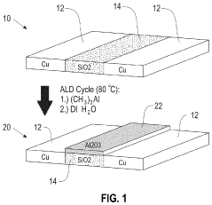
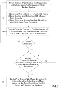
- The method involves contacting a substrate with a silicon dioxide surface and a zero-valent metal-containing surface with an organoaluminum compound at low temperatures, followed by exposure to water, to selectively form alumina on silicon dioxide surfaces without depositing on copper surfaces, using a database of ALD reactions to determine optimal conditions for selective deposition.
Regulatory Compliance Framework for ALD Manufacturing
The regulatory landscape for Atomic Layer Deposition (ALD) coating in high-tech manufacturing encompasses a complex matrix of international, national, and industry-specific standards. At the global level, organizations such as the International Organization for Standardization (ISO) have established frameworks like ISO 14644 for cleanroom environments where ALD processes typically occur. These standards define particulate cleanliness classifications, testing methodologies, and monitoring requirements essential for maintaining the ultra-pure environments necessary for high-quality ALD coating applications.
In the United States, the regulatory framework is primarily overseen by agencies including the Environmental Protection Agency (EPA), the Occupational Safety and Health Administration (OSHA), and the Food and Drug Administration (FDA) for medical applications. The EPA regulates chemical precursors used in ALD processes under the Toxic Substances Control Act (TSCA), with particular attention to potentially hazardous materials like trimethylaluminum (TMA) and various metal-organic compounds. OSHA standards address worker safety concerns related to chemical exposure, requiring proper ventilation systems, personal protective equipment, and emergency response protocols.
The European Union implements the Registration, Evaluation, Authorization and Restriction of Chemicals (REACH) regulation, which imposes stringent documentation and testing requirements for chemicals used in manufacturing processes, including ALD precursors. Additionally, the RoHS (Restriction of Hazardous Substances) directive limits the use of specific hazardous materials in electronic equipment, affecting ALD applications in semiconductor and electronics manufacturing.
For semiconductor applications specifically, the Semiconductor Equipment and Materials International (SEMI) organization provides industry standards that address equipment specifications, safety guidelines, and material handling protocols for ALD systems. These standards (such as SEMI S2 for equipment safety and SEMI S23 for chemical handling) have become de facto requirements for manufacturers operating in the global semiconductor supply chain.
Emerging regulatory considerations include nanomaterial safety regulations, as ALD processes create nanoscale films that may fall under increasing scrutiny from regulatory bodies. The EU's nanomaterial registry and similar initiatives in other regions require manufacturers to document and report nanomaterial usage, potentially affecting ALD coating operations.
Compliance with these diverse regulatory frameworks necessitates comprehensive management systems, including detailed documentation of process parameters, chemical inventories, exposure monitoring data, and waste management protocols. Many high-tech manufacturers implement ISO 14001 environmental management systems and ISO 45001 occupational health and safety management systems to systematically address regulatory requirements while maintaining operational efficiency.
Environmental Impact Assessment of ALD Processes
Atomic Layer Deposition (ALD) processes, while offering precision and efficiency in high-tech manufacturing, present significant environmental considerations that require thorough assessment. The environmental impact of ALD processes primarily stems from the precursor chemicals used, energy consumption, and waste generation. Precursors often include organometallic compounds, metal halides, and other reactive substances that may pose environmental hazards if not properly managed.
The gaseous emissions from ALD processes contain unreacted precursors and reaction byproducts that require effective abatement systems. These emissions may include volatile organic compounds (VOCs), particulate matter, and potentially hazardous air pollutants depending on the specific chemistry employed. Modern ALD facilities typically incorporate scrubbers, thermal oxidizers, or catalytic converters to mitigate these emissions, though the efficacy varies based on system design and maintenance protocols.
Water usage represents another environmental concern, particularly in semiconductor manufacturing where ultra-pure water is required for cleaning and processing. The purification of water for ALD applications consumes significant energy, while the resulting wastewater may contain trace metals and chemical residues requiring specialized treatment before discharge.
Energy consumption during ALD processes contributes substantially to their environmental footprint. The need for vacuum conditions, precise temperature control, and extended processing times results in considerable electricity usage. Life cycle assessments indicate that the operational energy requirements of ALD equipment often constitute the largest component of their environmental impact, particularly in regions where electricity generation relies heavily on fossil fuels.
Waste management challenges extend to the disposal of spent precursor containers, exhausted purification media, and maintenance materials. These items may contain residual chemicals requiring classification as hazardous waste, with associated regulatory compliance requirements and disposal costs. The semiconductor industry has established take-back programs for certain materials, though comprehensive circular economy approaches remain underdeveloped.
Regulatory frameworks governing ALD environmental impacts vary significantly across jurisdictions, creating compliance challenges for global manufacturers. While the European Union's REACH regulations and RoHS directive impose strict controls on chemical usage and waste, regulatory oversight in emerging manufacturing hubs may be less stringent, potentially creating regulatory arbitrage opportunities that undermine environmental protection goals.
Recent technological innovations are addressing these environmental concerns through the development of greener precursors with reduced toxicity, improved reactor designs that minimize precursor usage, and more efficient abatement systems. These advances, coupled with industry sustainability initiatives, suggest a trajectory toward reduced environmental impact as ALD technology continues to mature and expand into new manufacturing applications.
Unlock deeper insights with Patsnap Eureka Quick Research — get a full tech report to explore trends and direct your research. Try now!
Generate Your Research Report Instantly with AI Agent
Supercharge your innovation with Patsnap Eureka AI Agent Platform!