

Carbon Capture Sorbent Systems in Semiconductor Processing
OCT 21, 20259 MIN READ
Generate Your Research Report Instantly with AI Agent
PatSnap Eureka helps you evaluate technical feasibility & market potential.
Carbon Capture Technology Background and Objectives
Carbon capture technology has evolved significantly over the past decades, transitioning from theoretical concepts to practical applications across various industries. In the semiconductor manufacturing sector, carbon capture has emerged as a critical technology due to the industry's substantial carbon footprint, estimated at 2-3% of global emissions. The evolution of this technology has been driven by increasing regulatory pressures, corporate sustainability commitments, and the technical requirements of ultra-clean manufacturing environments.
The semiconductor industry utilizes various greenhouse gases in manufacturing processes, including perfluorocarbons (PFCs), sulfur hexafluoride (SF6), and nitrogen trifluoride (NF3), which have global warming potentials thousands of times greater than CO2. Traditional carbon capture technologies developed for power plants and industrial facilities have proven inadequate for semiconductor applications due to the unique composition of emission streams and the stringent purity requirements of cleanroom environments.
Sorbent-based carbon capture systems represent a promising approach for semiconductor manufacturing facilities. These systems utilize specialized materials that selectively adsorb carbon dioxide and other greenhouse gases from process exhaust streams. The technology has progressed from simple activated carbon systems to advanced materials including metal-organic frameworks (MOFs), zeolites, and functionalized polymers specifically engineered for semiconductor applications.
The primary technical objectives for carbon capture sorbent systems in semiconductor processing include achieving high capture efficiency (>90%) while maintaining minimal impact on production throughput and yield. Additionally, these systems must operate within the space constraints of existing fabs, demonstrate energy efficiency to avoid offsetting carbon benefits, and provide cost-effective operation to maintain competitive manufacturing costs in a margin-sensitive industry.
Recent technological advancements have focused on developing sorbents with high selectivity for specific process gases, rapid adsorption-desorption cycles, and resistance to contamination from process chemicals. Research is also exploring integration with existing abatement systems to create comprehensive emission control solutions that address both greenhouse gases and criteria pollutants simultaneously.
The semiconductor industry's roadmap for carbon neutrality has established ambitious targets, with many major manufacturers committing to net-zero emissions by 2040-2050. Carbon capture sorbent systems are expected to play a crucial role in this transition, particularly for difficult-to-abate emissions from essential manufacturing processes where alternative technologies are not yet viable.
Semiconductor Industry Demand for Carbon Capture Solutions
The semiconductor industry faces increasing pressure to reduce its carbon footprint amid growing environmental concerns and regulatory requirements. Manufacturing processes in this sector are energy-intensive and generate significant greenhouse gas emissions, particularly perfluorocarbons (PFCs), sulfur hexafluoride (SF6), nitrogen trifluoride (NF3), and carbon dioxide. These emissions contribute substantially to the industry's environmental impact, with some estimates suggesting that semiconductor manufacturing facilities can emit hundreds of thousands of metric tons of CO2 equivalent annually.
Market research indicates that the demand for carbon capture solutions in the semiconductor industry is driven by several factors. First, regulatory frameworks such as the Paris Agreement and regional carbon pricing mechanisms are compelling manufacturers to adopt cleaner production methods. The European Union's Carbon Border Adjustment Mechanism and similar policies in other regions are creating financial incentives for emissions reduction, directly affecting the semiconductor supply chain.
Consumer and investor pressure represents another significant market driver. Major technology companies that purchase semiconductors are increasingly setting ambitious carbon neutrality goals, extending these requirements to their suppliers. Investment funds with environmental, social, and governance (ESG) criteria are scrutinizing semiconductor manufacturers' sustainability practices, influencing capital flow toward companies with robust carbon management strategies.
The economic case for carbon capture in semiconductor manufacturing is strengthening. As carbon pricing mechanisms mature globally, the cost of unabated emissions is projected to increase substantially. Forward-thinking semiconductor manufacturers view carbon capture technologies not merely as compliance measures but as strategic investments that can provide competitive advantages through operational cost reduction and brand differentiation.
Industry analysts project that the market for specialized carbon capture solutions in semiconductor manufacturing could grow at a compound annual rate exceeding the broader carbon capture market due to the sector's unique technical requirements and high-value production environments. The demand is particularly strong for solutions that can be integrated into existing fabrication facilities with minimal disruption to production processes.
Geographically, demand is most pronounced in regions with concentrated semiconductor manufacturing capacity and stringent environmental regulations, notably East Asia, North America, and Europe. Taiwan, South Korea, Japan, and increasingly China represent significant potential markets, as these countries host major semiconductor manufacturing facilities while simultaneously strengthening their climate commitments.
Current Sorbent Systems and Technical Barriers
Current semiconductor manufacturing processes employ various carbon capture sorbent systems to manage emissions and maintain clean environments. Activated carbon remains the most widely used sorbent due to its high surface area, versatile pore structure, and relatively low cost. These systems typically achieve 80-90% removal efficiency for volatile organic compounds (VOCs) and other carbon-based contaminants in standard operating conditions. Zeolites represent another significant category, offering molecular sieve properties that enable selective adsorption based on molecular size and polarity, particularly valuable for precise gas separation in semiconductor fabrication.
Metal-organic frameworks (MOFs) have emerged as advanced sorbents with exceptional surface areas exceeding 7,000 m²/g and highly tunable pore structures. Despite their promising performance in laboratory settings, MOFs face stability challenges in the harsh chemical environments typical of semiconductor processing. Amine-functionalized silica materials provide another approach, with CO₂ capture capacities of 2-3 mmol/g under ambient conditions, though their regeneration typically requires significant energy input.
Despite these advances, current sorbent systems face substantial technical barriers. Thermal stability limitations represent a critical challenge, as many promising sorbents degrade at the high temperatures (often exceeding 400°C) encountered in semiconductor processing. This degradation leads to reduced capture efficiency and increased replacement frequency, significantly impacting operational costs.
Selectivity issues present another major obstacle, particularly in mixed gas streams containing multiple contaminants with similar physical properties. Current systems often struggle to selectively capture target compounds without also removing process-critical gases, creating inefficiencies in both capture and regeneration cycles.
Moisture sensitivity severely impacts many advanced sorbents, particularly MOFs and some amine-functionalized materials. Water vapor, ubiquitous in many semiconductor processes, can displace adsorbed carbon compounds or degrade the sorbent structure itself, dramatically reducing operational lifetimes from theoretical months to mere days or weeks in practical applications.
Regeneration energy requirements constitute a significant economic and environmental barrier. Most current systems require substantial thermal or pressure swing processes for regeneration, consuming 20-30% of the total energy budget for emission control systems. This high energy demand contradicts the sustainability goals driving carbon capture implementation.
Scale-up challenges further complicate industrial adoption, as many promising materials developed at laboratory scale encounter manufacturing difficulties, inconsistent performance, and prohibitive costs when produced at volumes necessary for semiconductor fabrication facilities.
Current Sorbent Material Solutions and Implementation
01 Amine-based sorbent systems for carbon capture
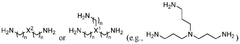
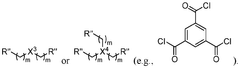
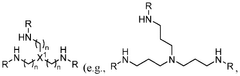
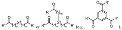
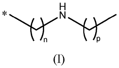
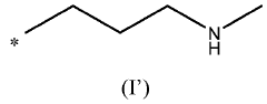
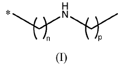
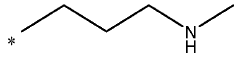
Amine-based sorbents are widely used in carbon capture systems due to their high CO2 selectivity and capacity. These systems typically involve amine compounds immobilized on porous supports such as silica or activated carbon. The amine functional groups react with CO2 through carbamate formation, enabling efficient capture from flue gases. Recent innovations focus on improving thermal stability, reducing regeneration energy, and preventing amine leaching during multiple capture-release cycles.- Metal-organic frameworks for carbon capture: Metal-organic frameworks (MOFs) are advanced porous materials that can be engineered for selective carbon dioxide adsorption. These crystalline structures combine metal ions with organic linkers to create highly tunable materials with exceptional surface areas and pore volumes. MOFs can be modified with specific functional groups to enhance CO2 selectivity and capacity, making them effective sorbents for carbon capture applications. Their regeneration capabilities and stability under various conditions make them promising candidates for industrial-scale carbon capture systems.
- Amine-functionalized sorbents: Amine-functionalized materials represent a significant class of carbon capture sorbents that operate through chemical adsorption mechanisms. These sorbents incorporate various amine groups onto support materials such as silica, activated carbon, or polymers to create strong binding sites for CO2. The amine functionality can be introduced through impregnation, grafting, or polymerization methods. These materials exhibit high CO2 selectivity even in humid conditions and can be designed with different amine types to optimize capture performance, capacity, and regeneration energy requirements.
- Direct air capture technologies: Direct air capture (DAC) technologies utilize specialized sorbent systems designed to extract CO2 directly from ambient air despite its low concentration. These systems employ highly selective sorbents with strong CO2 affinity, often arranged in optimized configurations to maximize air contact while minimizing energy consumption. DAC sorbents must overcome challenges related to the low CO2 concentration in air, moisture interference, and contaminant management. Advanced regeneration methods, including temperature or vacuum swing processes, are employed to release the captured CO2 for subsequent utilization or storage.
- Temperature-responsive sorbent systems: Temperature-responsive sorbent systems utilize materials that exhibit significant changes in CO2 adsorption capacity with temperature variations. These systems are designed to efficiently capture carbon dioxide at one temperature range and release it at another, enabling energy-efficient temperature swing adsorption processes. The sorbents may incorporate phase-change materials, thermally responsive polymers, or composite structures that optimize the energy requirements for the capture-release cycle. Advanced heat management strategies are integrated into these systems to minimize the overall energy penalty associated with sorbent regeneration.
- Hybrid and composite sorbent materials: Hybrid and composite sorbent materials combine multiple capture mechanisms or material types to achieve enhanced performance characteristics. These systems may integrate physical and chemical adsorption components, incorporate multiple functional groups, or combine organic and inorganic materials to create synergistic effects. Layered or hierarchical structures can be designed to optimize gas diffusion, adsorption kinetics, and capacity. These advanced materials often address multiple challenges simultaneously, such as selectivity in mixed gas streams, stability under cycling conditions, and resistance to contaminants, making them particularly valuable for complex industrial carbon capture applications.
02 Metal-organic frameworks (MOFs) for CO2 adsorption
Metal-organic frameworks represent an advanced class of porous materials with exceptional surface area and tunable pore structures for carbon capture. These crystalline materials consist of metal ions coordinated to organic ligands, creating three-dimensional structures with high CO2 selectivity. MOFs can be designed with specific functional groups to enhance CO2 binding affinity while maintaining regeneration efficiency. Their modular nature allows for precise engineering of adsorption properties to suit various carbon capture applications.Expand Specific Solutions03 Temperature-swing adsorption systems for carbon capture
Temperature-swing adsorption (TSA) systems utilize the temperature dependence of CO2 adsorption to capture and release carbon dioxide. These systems employ sorbents that adsorb CO2 at lower temperatures and release it when heated. The process typically involves multiple fixed beds operating in cycles to ensure continuous operation. Recent developments focus on reducing the energy requirements for the temperature swing, optimizing heat integration, and developing sorbents with faster kinetics to improve overall system efficiency.Expand Specific Solutions04 Zeolite-based carbon capture systems
Zeolites are crystalline aluminosilicate materials with well-defined pore structures that make them effective for carbon capture applications. Their high thermal stability and tunable surface properties allow for selective CO2 adsorption. Zeolite-based sorbent systems can be modified through ion exchange, impregnation with functional groups, or hierarchical structuring to enhance CO2 capture capacity and selectivity. These materials are particularly effective in pressure-swing adsorption systems and can be regenerated multiple times without significant performance degradation.Expand Specific Solutions05 Direct air capture sorbent technologies
Direct air capture (DAC) technologies employ specialized sorbents designed to extract CO2 directly from ambient air despite its low concentration. These systems typically use highly selective sorbents with strong CO2 binding properties, including functionalized polymers, alkali metal carbonates, and advanced composite materials. DAC sorbent systems often incorporate innovative contactor designs to maximize air-sorbent interaction while minimizing energy consumption. Recent developments focus on reducing regeneration energy requirements and developing materials that maintain performance under varying humidity and temperature conditions.Expand Specific Solutions
Leading Companies in Semiconductor Carbon Capture
Carbon capture sorbent systems in semiconductor processing are currently in an early growth phase, with market size expanding due to increasing environmental regulations and sustainability initiatives. The technology maturity varies across applications, with companies like Applied Materials, Schlumberger Technologies, and Samsung Electronics leading commercial implementations. Chinese entities including Huaneng Clean Energy Research Institute and CHN ENERGY Investment Group are making significant advancements in carbon capture integration with industrial processes. Academic institutions such as MIT, Rice University, and Norwegian University of Science & Technology are driving fundamental research innovations. The competitive landscape is characterized by a mix of established semiconductor equipment manufacturers, energy companies diversifying into green technologies, and specialized carbon capture startups like Compact Carbon Capture AS, creating a dynamic ecosystem of collaboration and competition.
CHN ENERGY Investment Group Co., Ltd.
Technical Solution: CHN ENERGY has adapted its extensive carbon capture expertise from power generation to develop specialized sorbent systems applicable to semiconductor manufacturing. Their technology utilizes advanced solid amine sorbents supported on mesoporous silica that demonstrate high CO2 adsorption capacity (>2.5 mmol/g) and excellent stability under the variable conditions found in semiconductor processing environments. CHN ENERGY's system employs a modular design that can be scaled according to the emission profile of different semiconductor manufacturing processes. Their solution incorporates a proprietary low-temperature steam regeneration process that operates at 90-110°C, significantly reducing energy requirements compared to conventional amine regeneration methods that typically require temperatures above 120°C. The company has also developed specialized sorbent formulations that maintain performance in the presence of trace amounts of fluorinated compounds and other specialty gases used in semiconductor fabrication.
Strengths: Extensive experience in large-scale carbon capture implementation; modular design allows for tailored solutions based on specific semiconductor processes; lower regeneration temperatures reduce energy consumption and operational costs. Weaknesses: Primary expertise in power generation rather than semiconductor manufacturing may affect integration; system size may be challenging for space-constrained semiconductor facilities; limited track record in high-purity applications required for semiconductor environments.
Schlumberger Technologies, Inc.
Technical Solution: Schlumberger Technologies has adapted its extensive carbon capture expertise from the energy sector to develop specialized sorbent systems for semiconductor manufacturing environments. Their approach utilizes advanced amine-functionalized silica sorbents that demonstrate exceptional CO2 capture efficiency (>90%) even at the low concentrations found in semiconductor fabrication facilities. The company's modular carbon capture units can be retrofitted to existing semiconductor processing tools, particularly those involved in chemical vapor deposition and etching processes where carbon-containing precursors are used. Schlumberger's system incorporates a proprietary sorbent regeneration technology that operates at lower temperatures (80-120°C) than conventional methods, reducing energy requirements by approximately 30%. Their solution also features real-time monitoring capabilities that track capture efficiency and sorbent degradation, allowing for optimized maintenance scheduling and performance verification.
Strengths: Proven expertise in carbon capture technology transferred from energy applications; modular design allows for flexible implementation; lower energy requirements for sorbent regeneration compared to competitors. Weaknesses: Limited semiconductor industry-specific experience may affect integration capabilities; system footprint may be challenging in space-constrained semiconductor fabs; higher initial costs compared to end-of-pipe solutions.
Key Patents and Innovations in Carbon Capture Sorbents
Entrapped small amines in nanoporous materials for gas capture
PatentWO2025101819A1
Innovation
- The development of sorbents comprising a porous substrate entrapping a plurality of amine compounds, with a polyamide film disposed on the substrate surface, enhances gas capture efficiency by entrapping amine compounds and preventing amine loss over time.
sorbent
PatentWO2024023158A1
Innovation
- A solid sorbent with secondary amines covalently attached to a silica support, optimized through specific grafting and water ratios, allowing for high CO2 adsorption capacity, long-term thermo-chemical stability, and low regeneration heat, using temperature swing adsorption with CO2 purge for desorption.
Environmental Regulations Impacting Carbon Management
The semiconductor industry faces increasingly stringent environmental regulations worldwide, particularly regarding carbon emissions and management. The Paris Agreement has established global targets for carbon reduction, with many countries implementing specific regulations that directly impact semiconductor manufacturing. In the United States, the Environmental Protection Agency (EPA) has expanded its oversight of perfluorocarbon (PFC) emissions, which are common byproducts in semiconductor processing and have global warming potentials thousands of times greater than CO2. The Clean Air Act amendments now require detailed reporting and reduction plans for these compounds.
The European Union's Emissions Trading System (EU ETS) has progressively tightened carbon allowances for industrial sectors, including semiconductor manufacturing. The EU's Carbon Border Adjustment Mechanism (CBAM) further impacts global supply chains by imposing carbon-related tariffs on imports from regions with less stringent environmental regulations. This creates significant economic incentives for implementing effective carbon capture technologies in semiconductor facilities operating in or exporting to European markets.
In Asia, where much of the world's semiconductor manufacturing occurs, countries like Japan, South Korea, and Taiwan have established their own carbon reduction frameworks. Japan's Carbon Pricing mechanism and South Korea's Emissions Trading Scheme specifically target high-energy industries, while Taiwan's Greenhouse Gas Reduction and Management Act sets mandatory reduction targets for semiconductor manufacturers, who represent a significant portion of the nation's industrial emissions.
Industry-specific standards are also emerging through organizations like the Semiconductor Industry Association (SIA) and the World Semiconductor Council (WSC). These bodies have established voluntary carbon reduction targets that often exceed regulatory requirements, responding to increasing pressure from investors and customers for environmental responsibility. The WSC's Best Practice Guidelines now include specific recommendations for carbon capture implementation in fabrication facilities.
Local permitting requirements present another regulatory layer, with many regions now requiring carbon management plans as prerequisites for facility expansion or new construction. Silicon Valley's Bay Area Air Quality Management District, for example, has implemented some of the world's most stringent requirements for semiconductor operations, mandating detailed accounting of process emissions and mitigation strategies.
These regulatory frameworks are evolving rapidly, with most jurisdictions accelerating their timelines for carbon neutrality goals. This regulatory landscape creates both compliance challenges and innovation opportunities for semiconductor manufacturers implementing carbon capture sorbent systems, as these technologies can serve as critical tools for meeting increasingly demanding emissions requirements while maintaining production capacity.
Economic Feasibility and ROI Analysis
The economic viability of implementing Carbon Capture Sorbent Systems (CCSS) in semiconductor manufacturing presents a complex investment landscape. Initial capital expenditure for these systems ranges from $2-5 million for medium-scale facilities, with larger fabs potentially facing investments of $8-12 million. This includes costs for sorbent materials, integration hardware, monitoring systems, and necessary facility modifications to accommodate carbon capture infrastructure.
Operating expenses add another significant financial dimension, typically ranging from $350,000-$750,000 annually. These costs encompass sorbent replacement cycles, energy consumption for regeneration processes, maintenance requirements, and specialized personnel training. The energy penalty associated with carbon capture operations—estimated at 2-4% of a facility's total energy consumption—further impacts ongoing operational costs.
Return on investment calculations reveal promising but variable outcomes. Semiconductor manufacturers implementing CCSS can expect breakeven periods of 4-7 years, depending on facility size, production volume, and regional carbon pricing mechanisms. Companies operating in regions with established carbon markets or carbon tax systems demonstrate accelerated ROI timelines, sometimes achieving breakeven in as little as 3 years.
The economic benefits extend beyond direct carbon reduction. Analysis of early adopters indicates that semiconductor manufacturers implementing CCSS have secured premium pricing from environmentally conscious customers, with price premiums ranging from 3-8% for "green semiconductor" products. Additionally, these companies report enhanced access to sustainability-focused investment capital and improved corporate valuation multiples.
Tax incentives and governmental support mechanisms significantly influence economic feasibility. In the United States, the 45Q tax credit provides up to $50 per metric ton of captured carbon, while the EU's Innovation Fund offers grants covering up to 60% of additional costs related to carbon capture implementation. Japan's Green Innovation Fund and South Korea's Green New Deal similarly provide substantial financial support for semiconductor manufacturers adopting carbon capture technologies.
Sensitivity analysis reveals that economic viability is most influenced by three factors: carbon pricing trajectories, technological efficiency improvements, and energy costs. Under current projections, CCSS implementations become universally economically viable across all major semiconductor manufacturing regions when carbon prices exceed $75-85 per ton, or when capture efficiency improves by 25-30% from current benchmarks.
Unlock deeper insights with PatSnap Eureka Quick Research — get a full tech report to explore trends and direct your research. Try now!
Generate Your Research Report Instantly with AI Agent
Supercharge your innovation with PatSnap Eureka AI Agent Platform!