

Characterization Techniques for 2D Semiconductor Heterostructures
OCT 21, 202510 MIN READ
Generate Your Research Report Instantly with AI Agent
PatSnap Eureka helps you evaluate technical feasibility & market potential.
2D Semiconductor Heterostructures Background and Objectives
Two-dimensional (2D) semiconductor heterostructures represent one of the most promising frontiers in materials science and semiconductor technology. Since the groundbreaking isolation of graphene in 2004, the field of 2D materials has expanded dramatically to include transition metal dichalcogenides (TMDs), hexagonal boron nitride (h-BN), black phosphorus, and numerous other atomically thin materials. The unique properties of these materials—including direct bandgaps, strong light-matter interactions, and exceptional carrier mobility—have positioned them as potential successors to traditional silicon-based technologies.
The evolution of 2D semiconductor technology has progressed through several distinct phases. Initially, research focused on single-layer materials and their fundamental properties. This was followed by the development of vertical heterostructures, often described as "van der Waals heterostructures," where different 2D materials are stacked layer by layer with atomic precision. Most recently, lateral heterostructures have emerged, where different 2D materials are seamlessly connected in-plane.
Characterization techniques for these complex structures have evolved in parallel with fabrication methods. Early characterization relied heavily on optical microscopy and Raman spectroscopy, while modern approaches incorporate advanced techniques such as scanning tunneling microscopy/spectroscopy (STM/STS), angle-resolved photoemission spectroscopy (ARPES), and various electron microscopy methods.
The primary objective of current characterization efforts is to develop comprehensive, non-destructive methods that can provide atomic-level structural information while simultaneously measuring electronic, optical, and mechanical properties. This multidimensional characterization is essential for understanding the complex physics at heterojunctions and interfaces, where novel phenomena often emerge.
Another critical goal is to establish standardized characterization protocols that enable reliable comparison between samples produced by different research groups. The lack of such standards has hindered progress in translating laboratory discoveries into practical applications.
Real-time, in-situ characterization represents another frontier, allowing researchers to observe dynamic processes during growth, device operation, or environmental interactions. This capability is particularly important for understanding degradation mechanisms and improving the stability of 2D heterostructures in ambient conditions.
Looking forward, the field aims to develop characterization techniques that can be scaled for industrial applications while maintaining atomic precision. This includes high-throughput methods compatible with wafer-scale production and quality control processes that can identify defects and inconsistencies across large areas.
The ultimate technical objective is to establish a complete characterization toolkit that bridges fundamental research and practical applications, accelerating the integration of 2D semiconductor heterostructures into next-generation electronic, optoelectronic, and quantum devices.
Market Applications and Demand Analysis for 2D Heterostructures
The market for 2D semiconductor heterostructures is experiencing rapid growth driven by increasing demand for miniaturized electronic components with enhanced performance characteristics. Current market estimates indicate that the global 2D materials market, including heterostructures, is expanding at a compound annual growth rate of approximately 30% through 2025, with particular acceleration in semiconductor applications.
Electronics and optoelectronics represent the primary application domains, with field-effect transistors (FETs) based on 2D heterostructures showing promise for overcoming silicon's scaling limitations. These ultra-thin transistors offer superior electrostatic control and reduced short-channel effects, making them attractive for next-generation computing architectures. Major semiconductor manufacturers are actively investigating these materials for integration into future chip designs.
Photonics and optoelectronic devices constitute another significant market segment. The direct bandgap nature of many 2D materials enables efficient light-matter interactions, while heterostructures allow precise bandgap engineering. This has led to development of photodetectors, light-emitting diodes, and photovoltaic cells with exceptional performance metrics. The telecommunications industry has shown particular interest in these materials for high-speed optical communication systems.
Energy storage and conversion applications represent an emerging market with substantial growth potential. Research indicates that 2D heterostructures can significantly enhance the performance of batteries, supercapacitors, and catalysts for hydrogen evolution reactions. Several energy companies have initiated R&D programs focused on commercializing these technologies within the next 3-5 years.
Quantum computing represents perhaps the most promising long-term market opportunity. The unique quantum properties of certain 2D heterostructures make them ideal platforms for quantum bits (qubits). While commercial quantum computing remains nascent, substantial investment is flowing into this sector, with 2D materials positioned as key enabling technologies.
Biomedical applications are also emerging as a significant market segment. The exceptional surface-to-volume ratio and tunable surface chemistry of 2D heterostructures make them promising candidates for biosensing, drug delivery, and tissue engineering applications. Several biotechnology companies have begun exploring these materials for next-generation diagnostic platforms.
Market analysis reveals regional variations in demand patterns. North America and Europe lead in research funding and patent applications, while Asia-Pacific countries, particularly China and South Korea, are rapidly expanding their manufacturing capabilities for 2D materials and devices. This geographic distribution suggests a globally competitive landscape developing around these advanced materials.
Current Characterization Techniques and Limitations
The characterization of 2D semiconductor heterostructures requires sophisticated analytical techniques to probe their unique physical, electronic, and optical properties. Currently, several advanced methods are employed, each with specific capabilities and inherent limitations.
Scanning probe microscopy (SPM) techniques, including atomic force microscopy (AFM) and scanning tunneling microscopy (STM), offer atomic-scale resolution for surface topography and electronic structure analysis. While AFM provides excellent topographical information and can measure mechanical properties, it lacks direct electronic structure information. STM offers superior electronic characterization but requires conductive samples and ultra-high vacuum conditions, limiting its applicability for certain heterostructure systems.
Electron microscopy techniques have become indispensable for 2D heterostructure characterization. Transmission electron microscopy (TEM) and scanning transmission electron microscopy (STEM) provide atomic-resolution imaging of crystal structures and interfaces. However, these techniques often require complex sample preparation that may alter the native structure of delicate 2D materials. Additionally, electron beam damage remains a significant challenge, particularly for beam-sensitive materials like transition metal dichalcogenides.
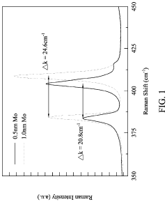
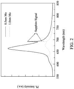
Optical characterization methods including Raman spectroscopy, photoluminescence (PL), and reflectance contrast measurements offer non-destructive probing of vibrational modes, electronic bandgap, and layer thickness. While these techniques provide valuable information about material quality and electronic properties, their spatial resolution is diffraction-limited, typically hundreds of nanometers, which is insufficient for nanoscale heterogeneities investigation.
X-ray based techniques such as X-ray photoelectron spectroscopy (XPS) and X-ray diffraction (XRD) provide elemental composition, chemical bonding states, and crystallographic information. However, conventional XPS has limited spatial resolution and surface sensitivity, while XRD requires relatively large sample areas for reliable measurements, challenging for small-scale 2D heterostructures.
Electrical transport measurements reveal carrier mobility, density, and quantum phenomena but often require complex device fabrication that can introduce defects and contamination. Contact resistance issues frequently complicate the interpretation of intrinsic material properties.
A significant limitation across multiple techniques is the challenge of in-situ and operando characterization. Most methods require specific sample environments (vacuum, low temperature) that differ from actual device operating conditions, creating a disconnect between measured properties and real-world performance.
The correlation of data across different characterization techniques remains challenging due to variations in sample preparation requirements, measurement conditions, and probed length scales. Developing unified frameworks for multi-technique data integration represents a critical frontier for comprehensive 2D heterostructure understanding.
Scanning probe microscopy (SPM) techniques, including atomic force microscopy (AFM) and scanning tunneling microscopy (STM), offer atomic-scale resolution for surface topography and electronic structure analysis. While AFM provides excellent topographical information and can measure mechanical properties, it lacks direct electronic structure information. STM offers superior electronic characterization but requires conductive samples and ultra-high vacuum conditions, limiting its applicability for certain heterostructure systems.
Electron microscopy techniques have become indispensable for 2D heterostructure characterization. Transmission electron microscopy (TEM) and scanning transmission electron microscopy (STEM) provide atomic-resolution imaging of crystal structures and interfaces. However, these techniques often require complex sample preparation that may alter the native structure of delicate 2D materials. Additionally, electron beam damage remains a significant challenge, particularly for beam-sensitive materials like transition metal dichalcogenides.
Optical characterization methods including Raman spectroscopy, photoluminescence (PL), and reflectance contrast measurements offer non-destructive probing of vibrational modes, electronic bandgap, and layer thickness. While these techniques provide valuable information about material quality and electronic properties, their spatial resolution is diffraction-limited, typically hundreds of nanometers, which is insufficient for nanoscale heterogeneities investigation.
X-ray based techniques such as X-ray photoelectron spectroscopy (XPS) and X-ray diffraction (XRD) provide elemental composition, chemical bonding states, and crystallographic information. However, conventional XPS has limited spatial resolution and surface sensitivity, while XRD requires relatively large sample areas for reliable measurements, challenging for small-scale 2D heterostructures.
Electrical transport measurements reveal carrier mobility, density, and quantum phenomena but often require complex device fabrication that can introduce defects and contamination. Contact resistance issues frequently complicate the interpretation of intrinsic material properties.
A significant limitation across multiple techniques is the challenge of in-situ and operando characterization. Most methods require specific sample environments (vacuum, low temperature) that differ from actual device operating conditions, creating a disconnect between measured properties and real-world performance.
The correlation of data across different characterization techniques remains challenging due to variations in sample preparation requirements, measurement conditions, and probed length scales. Developing unified frameworks for multi-technique data integration represents a critical frontier for comprehensive 2D heterostructure understanding.
State-of-the-Art Characterization Solutions
01 Optical characterization techniques for 2D semiconductor heterostructures
Various optical methods are employed to characterize 2D semiconductor heterostructures, including photoluminescence spectroscopy, Raman spectroscopy, and optical microscopy. These techniques provide valuable information about the electronic structure, layer thickness, defects, and interfacial properties of 2D materials. Advanced optical characterization allows for non-destructive analysis of heterostructure quality, band alignment, and quantum confinement effects that are critical for device performance.- Optical characterization techniques for 2D semiconductor heterostructures: Various optical methods are employed to characterize 2D semiconductor heterostructures, including photoluminescence spectroscopy, Raman spectroscopy, and optical microscopy. These techniques provide valuable information about the electronic structure, layer thickness, defects, and interfacial properties of 2D materials. Advanced optical characterization allows for non-destructive analysis of heterostructure quality, band alignment, and quantum confinement effects that are critical for device applications.
- Electron microscopy and spectroscopy for structural analysis: Electron microscopy techniques such as transmission electron microscopy (TEM), scanning electron microscopy (SEM), and scanning transmission electron microscopy (STEM) are widely used for structural characterization of 2D semiconductor heterostructures. These methods provide atomic-resolution imaging of interfaces, defects, and layer stacking. When combined with electron energy loss spectroscopy (EELS) and energy-dispersive X-ray spectroscopy (EDX), they offer detailed information about elemental composition and chemical bonding at interfaces.
- Scanning probe microscopy for surface and interface analysis: Scanning probe microscopy techniques, including atomic force microscopy (AFM), scanning tunneling microscopy (STM), and Kelvin probe force microscopy (KPFM), are essential for characterizing the surface morphology, electronic properties, and interfacial phenomena of 2D semiconductor heterostructures. These methods provide nanoscale resolution of surface topography, work function variations, and local electronic states, which are crucial for understanding the performance of devices based on these materials.
- X-ray and neutron-based characterization methods: X-ray diffraction (XRD), X-ray photoelectron spectroscopy (XPS), and neutron scattering techniques are employed to analyze the crystalline structure, chemical composition, and interfacial properties of 2D semiconductor heterostructures. These methods provide information about lattice parameters, strain distribution, layer orientation, and chemical bonding states. They are particularly valuable for non-destructive analysis of buried interfaces and large-area characterization of heterostructure uniformity.
- Electrical and optoelectronic property measurement techniques: Various techniques are used to characterize the electrical and optoelectronic properties of 2D semiconductor heterostructures, including Hall effect measurements, current-voltage characterization, capacitance-voltage profiling, and photoresponse measurements. These methods provide critical information about carrier mobility, concentration, transport mechanisms, band offsets, and quantum confinement effects. Advanced techniques such as scanning photocurrent microscopy and time-resolved spectroscopy offer insights into carrier dynamics and recombination processes at heterointerfaces.
02 Electron microscopy and diffraction techniques
Electron microscopy techniques, such as transmission electron microscopy (TEM), scanning electron microscopy (SEM), and scanning transmission electron microscopy (STEM), are crucial for visualizing the atomic structure and interfaces of 2D semiconductor heterostructures. These methods, combined with electron diffraction techniques, provide atomic-resolution imaging and crystallographic information about layer stacking, defects, and interfacial quality. High-resolution electron microscopy enables direct observation of atomic arrangements and structural properties that influence electronic behavior.Expand Specific Solutions03 Scanning probe microscopy for surface and interface analysis
Scanning probe microscopy techniques, including atomic force microscopy (AFM), scanning tunneling microscopy (STM), and Kelvin probe force microscopy (KPFM), are essential for characterizing the surface morphology, electronic properties, and interfacial characteristics of 2D semiconductor heterostructures. These methods provide nanoscale resolution of surface topography, electronic states, work function variations, and charge distribution across heterointerfaces, which are critical for understanding device performance and optimizing fabrication processes.Expand Specific Solutions04 Electrical and transport measurement techniques
Electrical characterization methods, including Hall effect measurements, current-voltage (I-V) characterization, and capacitance-voltage (C-V) profiling, are used to evaluate the electronic properties of 2D semiconductor heterostructures. These techniques provide information about carrier mobility, concentration, type, and transport mechanisms across heterointerfaces. Advanced electrical measurements can reveal quantum transport phenomena, band alignment, and interfacial electronic states that are crucial for developing high-performance electronic and optoelectronic devices.Expand Specific Solutions05 Spectroscopic and compositional analysis methods
Spectroscopic techniques such as X-ray photoelectron spectroscopy (XPS), energy-dispersive X-ray spectroscopy (EDX), and secondary ion mass spectrometry (SIMS) are employed to analyze the chemical composition, elemental distribution, and bonding states in 2D semiconductor heterostructures. These methods provide detailed information about material purity, interfacial reactions, and compositional gradients that affect electronic properties. Advanced spectroscopic analysis helps in optimizing growth processes and understanding degradation mechanisms in 2D heterostructure devices.Expand Specific Solutions
Leading Research Groups and Industry Players
The 2D semiconductor heterostructures characterization techniques market is in a growth phase, with increasing demand driven by advancements in quantum computing, electronics, and optoelectronics. Major players include established semiconductor giants like IBM, Samsung Electronics, and TSMC, who leverage their extensive R&D capabilities to develop advanced characterization methods. Specialized equipment manufacturers such as Carl Zeiss SMT and Tokyo Electron provide critical tools for atomic-level analysis. Research institutions like MIT and Interuniversitair Micro-Electronica Centrum collaborate with industry leaders to push technological boundaries. The field is witnessing rapid innovation in scanning probe microscopy, optical spectroscopy, and electron microscopy techniques, with companies competing to develop non-destructive, high-resolution methods for analyzing these ultra-thin materials.
International Business Machines Corp.
Technical Solution: IBM has developed a comprehensive multi-modal characterization platform for 2D semiconductor heterostructures that combines electrical, optical, and structural analysis techniques. Their approach utilizes ultra-high resolution transmission electron microscopy (TEM) with aberration correction to visualize atomic arrangements at heterointerfaces with sub-angstrom precision [1]. This is complemented by their proprietary scanning tunneling microscopy/spectroscopy (STM/STS) system that maps electronic states across heterostructures with atomic resolution while operating under controlled temperature and environmental conditions [2]. IBM has also pioneered the use of synchrotron-based X-ray techniques including grazing-incidence X-ray diffraction (GIXRD) and X-ray photoelectron spectroscopy (XPS) with depth profiling capabilities to characterize crystalline quality, strain distribution, and chemical composition throughout multilayer heterostructures [3]. Their platform integrates these measurements with electrical characterization using four-point probe techniques and Hall effect measurements specifically adapted for the ultra-thin nature of 2D materials, enabling correlation between structural properties and device performance [4].
Strengths: Comprehensive integration of multiple characterization techniques providing correlative insights; exceptional spatial resolution down to atomic scale; ability to perform in-situ measurements during device operation. Weaknesses: Extremely high equipment costs limiting accessibility; complex data integration requiring specialized expertise; some techniques require sample preparation that may alter material properties.
Carl Zeiss SMT GmbH
Technical Solution: Carl Zeiss has developed advanced electron microscopy solutions specifically optimized for 2D semiconductor heterostructure characterization. Their platform centers around aberration-corrected transmission electron microscopy (TEM) systems that achieve sub-50 picometer resolution, enabling direct visualization of atomic arrangements and interfacial structures in 2D heterostructures [1]. This is complemented by their proprietary energy-filtered TEM (EFTEM) technology that provides elemental mapping with nanometer spatial resolution, critical for analyzing compositional variations and interdiffusion at heterointerfaces [2]. Zeiss has also pioneered focused ion beam (FIB) sample preparation techniques specifically designed to minimize damage to delicate 2D materials, preserving their intrinsic properties during cross-sectional analysis [3]. Their systems incorporate in-situ holders that enable real-time observation of structural changes during heating, electrical biasing, or mechanical deformation, providing insights into dynamic processes at heterointerfaces [4]. Additionally, Zeiss has developed correlative microscopy workflows that integrate electron microscopy with optical spectroscopy and scanning probe techniques, enabling comprehensive characterization across multiple length scales [5].
Strengths: Exceptional spatial resolution allowing atomic-level visualization of interfaces; specialized sample preparation techniques preserving material integrity; capability for in-situ dynamic measurements under various stimuli. Weaknesses: Extremely high equipment and maintenance costs; requires highly specialized operators; sample preparation remains challenging despite advances; limited field of view compared to other techniques.
Key Technical Innovations in Nanoscale Characterization
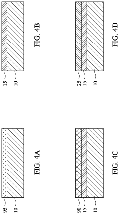
2d crystal hetero-structures and manufacturing methods thereof
PatentActiveUS20210005719A1
Innovation
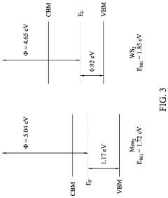
- The development of 2D crystal hetero-structures, specifically WS2/MoS2 hetero-structures, is achieved through chemical vapor deposition or sulfurization, enabling type-II band alignment and increased electron concentration by injecting electrons from WS2 to MoS2, thereby enhancing field-effect mobility and photoluminescence intensity.
Semiconductor heterostructure and method for forming same
PatentActiveUS20100264463A1
Innovation
- A method is introduced that includes an additional layer between the buffer and top layers with an in-plane lattice parameter between the first and second lattice parameters, and a reduced growth temperature for the additional and top layers, which reduces surface roughness without the need for additional polishing, thereby improving the smoothness of the heterostructure.


Standardization Challenges for 2D Material Characterization
The standardization of characterization techniques for 2D semiconductor heterostructures represents a significant challenge in the advancement of this field. Currently, there exists considerable variability in measurement protocols, sample preparation methods, and data reporting across research institutions and industrial laboratories. This inconsistency creates substantial barriers to reproducibility and comparative analysis, hindering the translation of laboratory discoveries into commercial applications.
A primary challenge lies in the establishment of universal sample preparation protocols. The atomically thin nature of 2D materials makes them exceptionally sensitive to environmental factors, substrate interactions, and processing conditions. Minor variations in exfoliation techniques, transfer methods, or cleaning procedures can dramatically alter material properties, leading to conflicting characterization results across different research groups.
Measurement standardization presents another critical hurdle. Techniques such as Raman spectroscopy, photoluminescence, and electrical transport measurements—all essential for characterizing 2D heterostructures—often employ different experimental parameters, equipment configurations, and data processing algorithms. The absence of standardized reference materials for calibration further compounds this issue, making direct comparison between studies problematic.
Data reporting conventions also lack uniformity across the field. Researchers frequently employ diverse metrics and presentation formats when documenting key parameters such as mobility, band alignment, or interfacial properties. This heterogeneity in reporting standards creates significant challenges for meta-analyses and systematic reviews, limiting the field's ability to establish reliable structure-property relationships.
International coordination efforts have begun addressing these standardization challenges, with organizations like ISO, NIST, and various academic consortia developing preliminary guidelines. However, the rapid evolution of 2D materials research often outpaces standardization initiatives, creating a persistent gap between cutting-edge research and established protocols.
The development of reference materials represents a promising approach to standardization. Creating well-characterized "standard" 2D heterostructures that can serve as benchmarks would enable more meaningful cross-laboratory comparisons. Similarly, round-robin testing programs, where identical samples are characterized across multiple facilities, could help identify and quantify measurement variabilities.
Addressing these standardization challenges requires collaborative efforts spanning academia, industry, and standards organizations. The establishment of consensus-based protocols for sample preparation, measurement, and data reporting would accelerate innovation by enabling more efficient knowledge transfer and reducing redundant research efforts in the rapidly evolving field of 2D semiconductor heterostructures.
Environmental Impact and Sustainability Considerations
The development and characterization of 2D semiconductor heterostructures carry significant environmental implications that warrant careful consideration. The fabrication processes for these advanced materials often involve hazardous chemicals, high-energy consumption, and rare earth elements, raising concerns about their ecological footprint. Chemical vapor deposition (CVD) and molecular beam epitaxy (MBE), common techniques for creating these heterostructures, require substantial energy inputs and may generate toxic byproducts that necessitate specialized disposal protocols.
Material efficiency represents another critical environmental dimension. Current fabrication methods typically yield considerable waste, with successful 2D heterostructure creation rates sometimes below 30%. This inefficiency translates to increased resource consumption and waste generation. Implementing closed-loop manufacturing systems and developing more precise deposition techniques could substantially reduce this environmental burden while improving economic viability.
The characterization techniques themselves also present environmental considerations. Electron microscopy, spectroscopy, and other advanced analytical methods often require cryogenic cooling agents, high vacuum systems, and significant power consumption. Research facilities are increasingly adopting energy-efficient equipment designs and implementing shared instrumentation programs to minimize these impacts while maintaining research capabilities.
Life cycle assessment (LCA) studies indicate that the environmental impact of 2D semiconductor heterostructures varies significantly depending on application context. When applied in energy harvesting technologies like high-efficiency photovoltaics or catalysts for water splitting, these materials can potentially offset their production footprint through operational benefits. Conversely, applications in consumer electronics may present less favorable environmental trade-offs without appropriate end-of-life management strategies.
End-of-life considerations remain particularly challenging for 2D heterostructures. Their complex compositions, often incorporating multiple elements in atomically thin layers, complicate recycling efforts. Research into selective chemical etching processes shows promise for recovering valuable components, though commercial-scale implementation remains distant. Extended producer responsibility frameworks may eventually incentivize design-for-recycling approaches in this field.
Sustainability certification standards specific to nanomaterials and 2D semiconductors are emerging but remain fragmented. Organizations like the International Organization for Standardization (ISO) and the Sustainable Electronics Manufacturing Working Group are developing frameworks to assess and certify environmental performance across the production lifecycle. These efforts aim to provide transparency and encourage continuous improvement in environmental stewardship within the rapidly evolving field of 2D semiconductor heterostructures.
Unlock deeper insights with PatSnap Eureka Quick Research — get a full tech report to explore trends and direct your research. Try now!
Generate Your Research Report Instantly with AI Agent
Supercharge your innovation with PatSnap Eureka AI Agent Platform!