Chiplet Architecture Influencing Modular System Design Strategies
JUL 16, 20259 MIN READ
Generate Your Research Report Instantly with AI Agent
Patsnap Eureka helps you evaluate technical feasibility & market potential.
Chiplet Evolution
The evolution of chiplet architecture represents a significant paradigm shift in the semiconductor industry, marking a transition from monolithic designs to modular, disaggregated approaches. This evolution began in the early 2010s as a response to the increasing challenges of traditional Moore's Law scaling. As transistor sizes approached physical limits, chipmakers sought alternative methods to improve performance and efficiency.
The initial phase of chiplet development focused on separating large, complex systems-on-chip (SoCs) into smaller, more manageable components. This approach allowed for better yield management and cost reduction by manufacturing different parts of a system using optimal process nodes. Companies like AMD pioneered this concept with their Zen-based processors, utilizing separate dies for CPU cores and I/O functions.
As the technology matured, the industry saw a proliferation of chiplet-based designs across various applications. High-performance computing, data centers, and artificial intelligence accelerators were among the first sectors to adopt chiplet architectures at scale. This adoption was driven by the need for increased computational power and memory bandwidth, which could be more efficiently achieved through modular designs.
The mid-2010s witnessed significant advancements in interconnect technologies, crucial for enabling efficient communication between chiplets. Standards like AMD's Infinity Fabric and Intel's EMIB (Embedded Multi-die Interconnect Bridge) emerged, providing high-bandwidth, low-latency connections between dies. These developments paved the way for more complex multi-chiplet systems, allowing for greater flexibility in system design and performance optimization.
By the late 2010s, chiplet architecture had become a mainstream strategy for many semiconductor companies. The focus shifted towards standardization and interoperability, with initiatives like DARPA's CHIPS (Common Heterogeneous Integration and IP Reuse Strategies) program promoting the development of modular, mix-and-match chiplet ecosystems. This era also saw the emergence of advanced packaging technologies, such as TSMC's CoWoS (Chip on Wafer on Substrate) and Intel's Foveros, which enabled 3D stacking of chiplets for even greater integration and performance density.
As we entered the 2020s, chiplet architecture continued to evolve, influencing not just processor design but entire system architectures. The concept of disaggregation extended beyond individual chips to encompass entire data center designs, with companies exploring modular, composable infrastructure based on chiplet principles. This trend has led to increased collaboration between semiconductor manufacturers, system integrators, and software developers to create holistic, scalable solutions that leverage the full potential of chiplet-based designs.
Market Demand Analysis
The market demand for Chiplet architecture and modular system design strategies has been growing rapidly in recent years, driven by the increasing complexity and cost of traditional monolithic chip designs. As the semiconductor industry approaches the limits of Moore's Law, chiplet-based designs offer a promising solution to continue scaling performance and functionality while managing costs and manufacturing challenges.
The global semiconductor market, valued at $555.9 billion in 2021, is expected to reach $1,033.5 billion by 2031, with a significant portion of this growth attributed to advanced packaging technologies, including chiplets. The demand for chiplet-based solutions is particularly strong in high-performance computing, data centers, and artificial intelligence applications, where the need for customization and scalability is paramount.
In the data center market, which is projected to grow at a CAGR of 10.5% from 2021 to 2028, chiplet architecture is gaining traction due to its ability to deliver higher performance, improved power efficiency, and reduced time-to-market for new products. Major cloud service providers and hyperscalers are actively exploring chiplet-based designs to meet the ever-increasing demands of their infrastructure.
The automotive industry is another key driver of chiplet demand, as advanced driver-assistance systems (ADAS) and autonomous vehicles require increasingly complex and powerful computing solutions. The automotive semiconductor market is expected to grow at a CAGR of 12.3% from 2021 to 2028, with chiplet-based designs playing a crucial role in meeting the stringent performance and reliability requirements of this sector.
Consumer electronics, particularly smartphones and wearables, are also contributing to the growing demand for chiplet architecture. As these devices continue to incorporate more advanced features and capabilities, manufacturers are turning to modular system designs to balance performance, power consumption, and form factor constraints.
The adoption of 5G technology is further fueling the demand for chiplet-based solutions, as network infrastructure and end-user devices require more sophisticated and flexible semiconductor designs to support the increased bandwidth and low latency requirements of next-generation wireless networks.
From a geographical perspective, North America and Asia-Pacific are the leading regions in terms of chiplet adoption and market demand. The United States, with its strong presence in the semiconductor industry and advanced research institutions, is at the forefront of chiplet innovation. Meanwhile, countries like Taiwan, South Korea, and China are rapidly expanding their capabilities in advanced packaging technologies to meet the growing global demand for chiplet-based solutions.
Technical Challenges
The adoption of chiplet architecture in modular system design presents several significant technical challenges that need to be addressed. One of the primary hurdles is the integration of multiple chiplets into a cohesive system. This requires advanced packaging technologies and interconnect solutions to ensure seamless communication between different chiplets while maintaining high performance and energy efficiency.
Thermal management poses another critical challenge in chiplet-based designs. As multiple chiplets are packed closely together, heat dissipation becomes more complex. Innovative cooling solutions and thermal design considerations are necessary to prevent performance degradation and ensure system reliability.
Power distribution and management across multiple chiplets present unique difficulties. Ensuring efficient power delivery to each chiplet while maintaining overall system power efficiency requires sophisticated power management techniques and careful system-level design considerations.
The design and implementation of high-speed, low-latency inter-chiplet communication interfaces are crucial for realizing the full potential of chiplet architectures. This involves developing advanced protocols and physical layer designs that can support the required bandwidth while minimizing latency and power consumption.
Testing and validation of chiplet-based systems introduce new complexities. Traditional testing methodologies may not be sufficient, necessitating the development of new approaches for both pre- and post-integration testing to ensure system reliability and performance.
Standardization of chiplet interfaces and protocols remains a significant challenge. The lack of widely adopted industry standards can hinder interoperability between chiplets from different vendors, potentially limiting the flexibility and modularity that chiplet architectures aim to provide.
Software optimization for chiplet-based systems presents another hurdle. Existing software may not be optimized to take full advantage of the distributed nature of chiplet architectures, requiring new programming models and tools to effectively utilize the modular hardware resources.
Yield management in chiplet production introduces unique challenges compared to monolithic designs. While chiplet architectures can potentially improve overall yield, managing the yield of individual chiplets and ensuring compatibility in the final integrated system requires sophisticated yield management strategies.
Lastly, the design of efficient and flexible system-level architectures that can fully leverage the modularity of chiplets remains an ongoing challenge. This includes developing adaptive system management techniques that can dynamically optimize performance and power efficiency across multiple chiplets based on workload requirements.
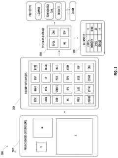
Current Solutions
01 Modular chiplet architecture design
Chiplet architecture employs a modular approach to system design, allowing for the integration of multiple smaller chips (chiplets) into a single package. This design methodology enables greater flexibility, scalability, and cost-effectiveness in creating complex systems-on-chip (SoCs). By separating different functionalities into individual chiplets, manufacturers can mix and match components to create customized solutions for various applications.- Modular chiplet architecture design: This approach involves designing a system using multiple smaller chips (chiplets) that can be combined in a modular fashion. It allows for greater flexibility, scalability, and cost-effectiveness in system design. The modular nature enables mixing and matching of different chiplets to create customized solutions for various applications.
- Interconnect technologies for chiplet integration: Advanced interconnect technologies are crucial for efficient communication between chiplets. This includes high-bandwidth, low-latency interfaces and packaging solutions that enable seamless integration of multiple chiplets. These technologies address challenges in data transfer, power efficiency, and thermal management in chiplet-based systems.
- Power management and thermal optimization: Effective power management and thermal optimization are essential in chiplet-based designs. This involves developing strategies for distributing power efficiently across multiple chiplets and managing heat dissipation. Advanced cooling solutions and power-aware design techniques are employed to ensure optimal performance and reliability of the modular system.
- System-level integration and testing: Integrating multiple chiplets into a cohesive system requires sophisticated design and testing methodologies. This includes developing system-level simulation tools, implementing effective testing strategies for individual chiplets and the integrated system, and ensuring compatibility and performance across different chiplet combinations.
- Standardization and interoperability: Establishing industry standards for chiplet interfaces and protocols is crucial for the widespread adoption of chiplet architecture. This involves developing common specifications for chiplet-to-chiplet communication, packaging, and system integration. Standardization efforts aim to ensure interoperability between chiplets from different manufacturers and facilitate a robust ecosystem for modular system design.
02 Interconnect technologies for chiplet integration
Advanced interconnect technologies play a crucial role in chiplet-based designs, facilitating high-speed, low-latency communication between different chiplets within a package. These interconnects may include die-to-die (D2D) interfaces, through-silicon vias (TSVs), and advanced packaging techniques. The development of efficient and standardized interconnect solutions is essential for realizing the full potential of chiplet architectures.Expand Specific Solutions03 Power management and thermal considerations
Effective power management and thermal design are critical aspects of chiplet-based systems. As multiple chiplets are integrated into a single package, managing power consumption and heat dissipation becomes more complex. Innovative cooling solutions, power gating techniques, and intelligent power distribution strategies are employed to ensure optimal performance and reliability of chiplet-based designs.Expand Specific Solutions04 Design and verification methodologies
Chiplet-based system design requires specialized design and verification methodologies to address the unique challenges of modular architectures. This includes developing tools and processes for chiplet-level design, system-level integration, and comprehensive verification of the entire multi-chiplet system. Advanced simulation and emulation techniques are employed to ensure proper functionality and performance of the integrated system.Expand Specific Solutions05 Standardization and ecosystem development
The development of industry standards and a robust ecosystem is crucial for the widespread adoption of chiplet-based architectures. This includes efforts to standardize chiplet interfaces, packaging technologies, and design methodologies. Collaboration between semiconductor companies, foundries, and tool vendors is essential to create a cohesive ecosystem that supports the design, manufacturing, and integration of chiplet-based systems across various applications and industries.Expand Specific Solutions
Key Industry Players
The chiplet architecture market is in a growth phase, driven by increasing demand for modular system designs in high-performance computing and AI applications. The market size is expanding rapidly, with major players like Intel, AMD, and TSMC investing heavily in chiplet technologies. The technical maturity varies, with some companies like Intel and AMD already offering commercial products, while others are still in research and development stages. Companies such as Micron, Applied Materials, and MediaTek are also making significant strides in chiplet-related technologies, contributing to a competitive and dynamic landscape. As the technology evolves, we can expect to see more diverse applications and increased adoption across various sectors of the semiconductor industry.
Intel Corp.
Technical Solution: Intel's Foveros 3D packaging technology is a key component of their chiplet architecture strategy. This advanced packaging method allows for the vertical stacking of multiple chiplets, enabling higher performance and lower power consumption[1]. Intel's Meteor Lake processors utilize this technology, combining compute, graphics, and AI tiles into a single package[2]. The company has also introduced their Universal Chiplet Interconnect Express (UCIe) standard, which aims to create an open ecosystem for chiplet-based designs, allowing for mix-and-match of chiplets from different vendors[3].
Strengths: Advanced 3D packaging technology, open ecosystem approach with UCIe. Weaknesses: Relatively new to chiplet architecture compared to some competitors, potential challenges in ecosystem adoption.
Taiwan Semiconductor Manufacturing Co., Ltd.
Technical Solution: TSMC's chiplet architecture approach focuses on their advanced packaging technologies, including Integrated Fan-Out (InFO) and Chip-on-Wafer-on-Substrate (CoWoS). These technologies enable the integration of multiple chips in a single package, improving performance and reducing power consumption[4]. TSMC's 3DFabric platform combines front-end and back-end technologies to support various chiplet integration schemes, allowing for customized solutions for different applications[5]. The company has also developed their System-on-Integrated-Chips (SoIC) technology, which enables ultra-high-density 3D chip stacking with micron-scale bumps[6].
Strengths: Industry-leading process nodes, diverse advanced packaging options. Weaknesses: Reliance on partnerships for full system integration, potential geopolitical risks.
Core Innovations
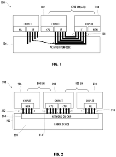
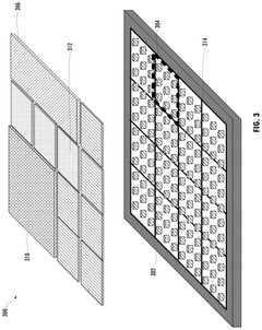
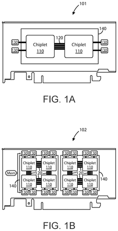
Modular chiplet system
PatentPendingUS20250029971A1
Innovation
- The modular chiplet system employs an active semiconductor substrate with a network-on-chip and a fabric device that includes a built-in network-on-chip, 3D chiplet interfaces, and a library of rotationally symmetrical chiplets. This system reduces lateral communication distances, enables efficient packet routing, and allows for the creation of various system permutations using a small set of chiplets and fabric devices.
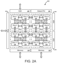
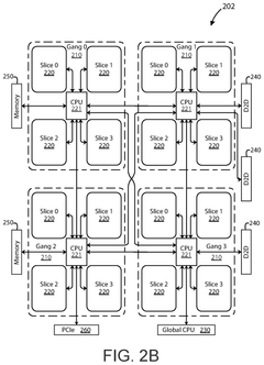
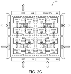
Ai accelerator apparatus using full mesh connectivity chiplet devices for transformer workloads
PatentPendingUS20250123984A1
Innovation
- The development of an AI accelerator apparatus with a modular chiplet architecture, featuring in-memory compute and full mesh connectivity, which includes multiple chiplets coupled in a full mesh configuration, each with tiles and slices that integrate CPU, DIMC, and hardware dispatch devices, optimizing computational performance and reducing power consumption.
Standardization Efforts
Standardization efforts in chiplet architecture are crucial for enabling interoperability and fostering a robust ecosystem for modular system design. The industry has recognized the need for common interfaces and protocols to facilitate seamless integration of chiplets from different vendors. Several initiatives have emerged to address this challenge and drive the adoption of chiplet-based designs.
One of the most prominent standardization efforts is the Universal Chiplet Interconnect Express (UCIe) consortium. Launched in 2022, UCIe aims to establish an open industry standard for die-to-die interconnects. The consortium includes major players such as Intel, AMD, Arm, TSMC, and Samsung, among others. UCIe focuses on defining physical and protocol layers for chiplet interconnects, enabling a plug-and-play approach to chiplet integration.
Another significant initiative is the Open Compute Project's (OCP) Chiplet Design Exchange (CDX) working group. CDX aims to develop standards for chiplet-based designs, focusing on areas such as thermal management, power delivery, and signal integrity. The group's efforts complement UCIe by addressing system-level challenges in chiplet integration.
The CHIPS Alliance, an open-source hardware initiative, has also been active in promoting standardization in chiplet design. Their Chisel hardware construction language and the Rocket Chip generator provide tools and methodologies for creating modular and reusable chiplet designs.
In addition to these industry-wide efforts, individual companies have been developing their own chiplet interconnect technologies. AMD's Infinity Fabric and Intel's Advanced Interface Bus (AIB) are examples of proprietary solutions that have paved the way for chiplet-based designs. While these technologies are not open standards, they have influenced the direction of industry-wide standardization efforts.
The IEEE has also recognized the importance of chiplet standardization and has initiated the P3047 working group. This group aims to develop standards for chiplet interfaces and protocols, complementing the work of other industry initiatives.
As standardization efforts progress, we can expect to see increased interoperability between chiplets from different vendors. This will likely lead to a more diverse and competitive market for chiplet-based solutions, ultimately driving innovation in modular system design. However, challenges remain in areas such as testing and verification of multi-vendor chiplet systems, as well as in ensuring consistent performance across different chiplet combinations.
The success of these standardization efforts will be critical in realizing the full potential of chiplet architecture in modular system design. As the industry converges on common standards, we can anticipate accelerated adoption of chiplet-based designs across a wide range of applications, from high-performance computing to edge devices and beyond.
Economic Impact
The economic impact of chiplet architecture on modular system design strategies is profound and far-reaching. This innovative approach to semiconductor design and manufacturing has the potential to reshape the economics of the entire industry, offering significant cost savings and improved performance across various sectors.
Chiplet architecture allows for the disaggregation of complex system-on-chip (SoC) designs into smaller, more manageable components. This modular approach enables manufacturers to mix and match different chiplets, potentially from various suppliers, to create customized solutions. The economic implications of this strategy are substantial, as it reduces the need for expensive monolithic chip designs and allows for more flexible and cost-effective production processes.
One of the primary economic benefits of chiplet-based modular system design is the potential for improved yield rates. By manufacturing smaller, less complex chiplets rather than large, monolithic chips, manufacturers can achieve higher yields and reduce waste. This translates to lower production costs and increased profitability for semiconductor companies. Additionally, the ability to reuse chiplet designs across multiple products can significantly reduce research and development expenses, allowing companies to amortize design costs over a larger product portfolio.
The modular nature of chiplet-based systems also introduces new economic models for the semiconductor industry. It opens up opportunities for specialized chiplet manufacturers to emerge, focusing on specific functionalities or technologies. This specialization can lead to increased competition and innovation in the market, potentially driving down costs for end-users while improving overall system performance.
Furthermore, chiplet architecture enables more efficient supply chain management. Companies can source chiplets from multiple suppliers, reducing dependency on a single manufacturer and mitigating supply chain risks. This diversification can lead to more stable pricing and improved negotiating power for system integrators.
The economic impact extends beyond the semiconductor industry itself. Industries relying on advanced computing systems, such as data centers, telecommunications, and automotive, stand to benefit from the cost savings and performance improvements offered by chiplet-based designs. This could accelerate the adoption of emerging technologies like artificial intelligence, 5G networks, and autonomous vehicles, driving economic growth across multiple sectors.
However, the transition to chiplet-based modular system design is not without economic challenges. Significant investments in new design tools, manufacturing processes, and testing methodologies are required. Additionally, the industry must develop standardized interfaces and protocols to ensure interoperability between chiplets from different manufacturers. These upfront costs may initially offset some of the economic benefits, but the long-term advantages are expected to outweigh these short-term investments.
Unlock deeper insights with Patsnap Eureka Quick Research — get a full tech report to explore trends and direct your research. Try now!
Generate Your Research Report Instantly with AI Agent
Supercharge your innovation with Patsnap Eureka AI Agent Platform!