Chiplet Design: Essential Strategies for Cutting Edge Breakthroughs
JUL 16, 20259 MIN READ
Generate Your Research Report Instantly with AI Agent
Patsnap Eureka helps you evaluate technical feasibility & market potential.
Chiplet Evolution and Objectives
Chiplet technology has emerged as a revolutionary approach in semiconductor design, offering a paradigm shift in how integrated circuits are conceived and manufactured. The evolution of chiplets can be traced back to the early 2010s when traditional monolithic chip designs began to face significant challenges in terms of scalability, performance, and cost-effectiveness.
The primary objective of chiplet design is to overcome the limitations of monolithic chip architectures by disaggregating complex systems into smaller, more manageable components. This approach allows for greater flexibility in design, improved yield, and the ability to mix and match different process nodes within a single package. As Moore's Law slows down, chiplets provide a viable path forward for continued performance improvements and cost reductions in the semiconductor industry.
The evolution of chiplet technology has been marked by several key milestones. Initially, the focus was on developing reliable interconnect technologies to enable high-bandwidth, low-latency communication between chiplets. This led to the development of advanced packaging technologies such as 2.5D and 3D integration. Concurrently, industry standards like Universal Chiplet Interconnect Express (UCIe) have emerged to facilitate interoperability between chiplets from different vendors.
As the technology matured, chiplet designs have found applications across a wide range of computing domains, from high-performance processors to specialized AI accelerators. The flexibility offered by chiplets has enabled companies to rapidly iterate on designs and bring products to market faster, while also allowing for more customized solutions tailored to specific application needs.
Looking ahead, the objectives for chiplet technology are multifaceted. One key goal is to further improve the energy efficiency of chiplet-based systems, addressing the growing concerns around power consumption in data centers and mobile devices. Another objective is to enhance the scalability of chiplet designs, enabling even more complex systems to be built using this modular approach.
Additionally, there is a push towards developing more advanced integration technologies, such as wafer-level fan-out packaging and silicon photonics, to further improve the performance and density of chiplet-based systems. The industry is also working towards more standardized interfaces and design methodologies to streamline the chiplet ecosystem and reduce development costs.
In conclusion, the evolution of chiplet technology represents a significant shift in semiconductor design philosophy, with objectives aimed at addressing the challenges of modern computing while paving the way for future innovations in integrated circuit design and manufacturing.
Market Demand Analysis for Chiplet Solutions
The market demand for chiplet solutions has been experiencing significant growth, driven by the increasing complexity and performance requirements of modern computing systems. As traditional monolithic chip designs approach their physical limits, chiplets offer a promising alternative that allows for more flexible and scalable semiconductor architectures.
The global chiplet market is projected to expand rapidly, with estimates suggesting a compound annual growth rate (CAGR) of over 40% in the coming years. This growth is fueled by the rising demand for high-performance computing in various sectors, including data centers, artificial intelligence, 5G networks, and edge computing. The ability of chiplets to enable modular design and improve yield rates has made them particularly attractive to semiconductor manufacturers and system integrators.
In the data center segment, chiplets are gaining traction due to their potential to deliver higher performance and energy efficiency. Major cloud service providers and enterprise customers are increasingly adopting chiplet-based solutions to meet the growing computational demands of AI and machine learning workloads. This trend is expected to continue as data centers seek to optimize their infrastructure for emerging applications.
The automotive industry is another key driver of chiplet demand, particularly in the context of advanced driver-assistance systems (ADAS) and autonomous vehicles. These applications require sophisticated processing capabilities that can be efficiently delivered through chiplet-based architectures. As the automotive sector continues its transition towards electrification and autonomy, the demand for chiplet solutions is likely to surge.
Consumer electronics, including smartphones, tablets, and wearables, represent another significant market for chiplet technology. The need for improved performance, reduced power consumption, and smaller form factors aligns well with the advantages offered by chiplets. As consumers increasingly demand devices with AI capabilities and enhanced multimedia features, chiplet-based designs are poised to play a crucial role in meeting these expectations.
The industrial and IoT sectors are also contributing to the growing demand for chiplet solutions. Smart manufacturing, industrial automation, and the proliferation of connected devices are driving the need for more powerful and efficient edge computing solutions. Chiplets offer the flexibility and scalability required to address the diverse requirements of these applications.
Despite the promising outlook, challenges remain in the widespread adoption of chiplet technology. Standardization efforts, such as those led by industry consortia, are crucial for ensuring interoperability and reducing integration complexities. Additionally, the development of advanced packaging technologies and design tools will be essential to fully realize the potential of chiplet-based architectures.
In conclusion, the market demand for chiplet solutions is robust and multifaceted, spanning various industries and applications. As the technology matures and ecosystem support grows, chiplets are expected to play an increasingly important role in shaping the future of semiconductor design and manufacturing.
Chiplet Technology Landscape and Challenges
Chiplet technology has emerged as a revolutionary approach in semiconductor design, offering a paradigm shift in how complex integrated circuits are conceived and manufactured. This innovative methodology involves breaking down large, monolithic chip designs into smaller, more manageable components called chiplets. These chiplets can be manufactured separately and then integrated onto a single package, allowing for greater flexibility, improved yield, and potentially lower costs in chip production.
The current landscape of chiplet technology is characterized by rapid advancements and growing adoption across the semiconductor industry. Major players such as AMD, Intel, and TSMC have embraced chiplet designs in their high-performance processors and systems-on-chip (SoCs). This trend is driven by the increasing demand for more powerful and efficient computing solutions, particularly in data centers, artificial intelligence, and high-performance computing applications.
Despite its promising potential, chiplet technology faces several significant challenges. One of the primary hurdles is the development of standardized interfaces for chiplet-to-chiplet communication. While initiatives like the Universal Chiplet Interconnect Express (UCIe) consortium are working towards establishing industry-wide standards, the lack of universal protocols still hinders widespread interoperability between chiplets from different manufacturers.
Another critical challenge lies in the realm of thermal management and power distribution. As chiplets are integrated more densely, managing heat dissipation and ensuring efficient power delivery across the package becomes increasingly complex. This necessitates innovative cooling solutions and advanced power delivery networks to maintain optimal performance and reliability.
The design and verification of chiplet-based systems present their own set of challenges. Engineers must grapple with the complexities of integrating multiple chiplets, each potentially manufactured using different process nodes. This heterogeneous integration requires sophisticated design tools and methodologies to ensure seamless functionality and performance optimization across the entire system.
Testing and quality assurance for chiplet-based designs also pose unique challenges. Traditional testing methods may not be sufficient to verify the intricate interactions between chiplets, necessitating the development of new testing strategies and equipment capable of assessing both individual chiplets and the integrated system as a whole.
As the chiplet ecosystem continues to evolve, addressing these challenges will be crucial for realizing the full potential of this technology. Collaborative efforts across the industry, including standardization initiatives, advancements in packaging technologies, and the development of specialized design and testing tools, will play a pivotal role in overcoming these hurdles and driving the widespread adoption of chiplet-based architectures in next-generation semiconductor products.
Current Chiplet Design Methodologies
01 Advanced Interconnect Technologies for Chiplets
Cutting-edge breakthroughs in chiplet design focus on developing advanced interconnect technologies. These innovations aim to improve the communication between different chiplets, enhancing overall system performance and efficiency. New interconnect solutions include high-bandwidth interfaces, optical interconnects, and 3D stacking technologies that enable faster data transfer and reduced latency between chiplets.- Advanced Interconnect Technologies for Chiplets: Cutting-edge interconnect technologies are being developed to enhance communication between chiplets. These include high-bandwidth interfaces, advanced packaging techniques, and novel die-to-die connection methods. These innovations aim to reduce latency, increase data transfer rates, and improve overall system performance in multi-chiplet designs.
- Heterogeneous Integration of Chiplets: Breakthroughs in heterogeneous integration allow for the combination of chiplets manufactured using different process nodes or technologies. This approach enables the optimization of performance, power efficiency, and cost by utilizing the most suitable manufacturing process for each chiplet function within a single package.
- Thermal Management Solutions for Chiplet Designs: Innovative thermal management techniques are being developed to address the heat dissipation challenges in densely packed chiplet designs. These solutions include advanced cooling systems, thermal interface materials, and intelligent power management strategies to maintain optimal operating temperatures and ensure reliability.
- AI-Driven Chiplet Design and Optimization: Artificial intelligence and machine learning algorithms are being employed to optimize chiplet designs, interconnect topologies, and system-level integration. These AI-driven approaches help in rapid design space exploration, performance prediction, and automatic optimization of complex multi-chiplet systems.
- 3D Stacking and Packaging Innovations for Chiplets: Advancements in 3D stacking and packaging technologies are enabling more compact and efficient chiplet-based designs. These innovations include through-silicon vias (TSVs), interposers, and novel bonding techniques that allow for vertical integration of chiplets, resulting in reduced form factors and improved performance.
02 Heterogeneous Integration of Chiplets
Chiplet design breakthroughs involve the integration of diverse types of chiplets, each optimized for specific functions. This heterogeneous integration allows for the combination of chiplets manufactured using different process nodes, enabling the creation of highly customized and efficient system-on-chip (SoC) designs. The approach facilitates the integration of specialized accelerators, memory, and processing units on a single package.Expand Specific Solutions03 Thermal Management and Power Optimization in Chiplet Designs
Innovative thermal management and power optimization techniques are being developed for chiplet-based designs. These advancements focus on efficiently dissipating heat generated by densely packed chiplets and optimizing power distribution across the system. New cooling solutions and power management strategies are being implemented to ensure reliable operation and maximize performance of multi-chiplet packages.Expand Specific Solutions04 AI-Driven Chiplet Design and Optimization
Artificial intelligence and machine learning techniques are being leveraged to optimize chiplet designs. These AI-driven approaches assist in the placement and routing of chiplets, predict performance characteristics, and optimize the overall system architecture. The use of AI in chiplet design processes enables faster iteration and more efficient exploration of design spaces, leading to improved performance and reduced time-to-market.Expand Specific Solutions05 Standardization and Interoperability in Chiplet Ecosystems
Efforts are being made to establish industry standards for chiplet interfaces and packaging technologies. These standardization initiatives aim to create a more open and interoperable chiplet ecosystem, allowing for easier integration of chiplets from different vendors. The development of common interfaces and protocols facilitates the creation of modular and scalable chiplet-based systems across various applications and industries.Expand Specific Solutions
Key Players in Chiplet Industry
The chiplet design market is in a dynamic growth phase, driven by increasing demand for high-performance computing and AI applications. Major players like Intel, NVIDIA, AMD (through Xilinx), and TSMC are investing heavily in this technology, indicating its strategic importance. The market size is expanding rapidly, with projections suggesting significant growth in the coming years. Technologically, chiplet design is maturing, with companies like Micron, Qualcomm, and Huawei also making strides. However, challenges in standardization and integration persist, keeping the field competitive and innovative. The involvement of diverse players from semiconductor, telecommunications, and AI sectors underscores the technology's broad applicability and potential for cross-industry disruption.
Intel Corp.
Technical Solution: Intel's Chiplet Design strategy focuses on their Foveros 3D packaging technology, which allows for vertical stacking of chiplets. This approach enables the integration of heterogeneous architectures and process nodes within a single package. Intel's Meteor Lake processors utilize this technology, combining compute, graphics, and AI tiles manufactured on different process nodes[1]. The company has also introduced their EMIB (Embedded Multi-die Interconnect Bridge) technology, which provides high-bandwidth, short-reach interconnects between chiplets in a 2.5D configuration[2]. This allows for more efficient die-to-die communication compared to traditional interposers.
Strengths: Vertical integration capabilities, advanced packaging technologies. Weaknesses: Potential yield issues with complex 3D stacking, higher initial costs compared to monolithic designs.
Huawei Technologies Co., Ltd.
Technical Solution: Huawei's approach to Chiplet Design is exemplified in their Kirin series processors. The company has developed a custom interconnect technology called "Super Die-to-Die" (SD2D) for high-bandwidth, low-latency communication between chiplets[3]. Huawei's chiplet strategy focuses on disaggregating SoC components into separate dies, allowing for more flexible combinations of IP blocks and potentially improving yield. Their recent Kirin 9000 series utilizes this approach, integrating AI, 5G, and CPU components as separate chiplets[4].
Strengths: Custom interconnect technology, flexibility in IP integration. Weaknesses: Geopolitical challenges affecting supply chain, potential limitations in accessing advanced manufacturing processes.
Breakthrough Chiplet Technologies
On-demand programmable atomic kernel loading
PatentWO2022086807A1
Innovation
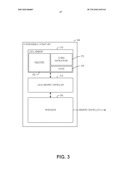
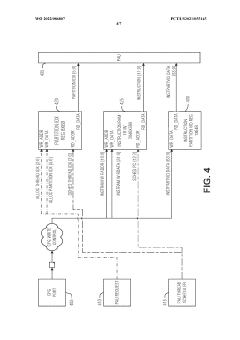
- Implementing an on-demand mechanism for loading PAO kernels, where PAUs register for potential use and reserve space, loading the kernel only when requested, and signaling a trap to initiate kernel transfer when needed.
Multiple protocol header processing
PatentWO2022046261A1
Innovation
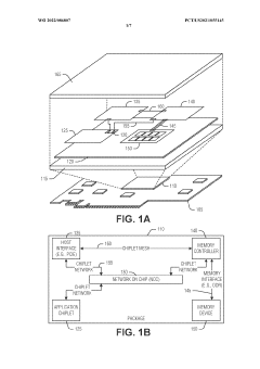
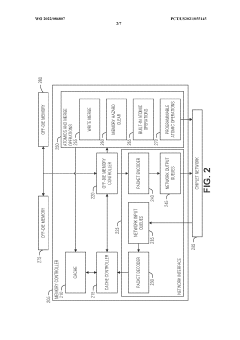
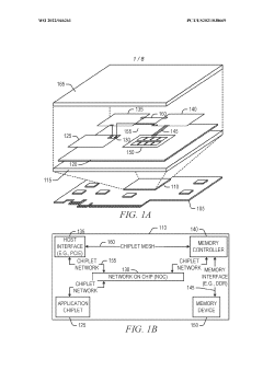
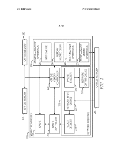
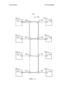
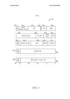
- The implementation of a header processing system that includes a bridge type (BTYPE) field to identify the protocol, allowing for the interpretation of command fields differently based on this field, enabling a single network to carry packets of various protocols without encapsulation, and utilizing a chiplet system with a chiplet protocol interface (CPI) for efficient inter-chiplet communication.
Chiplet Standardization Efforts
Chiplet standardization efforts have become increasingly crucial in the semiconductor industry as the demand for more complex and efficient chip designs continues to grow. These efforts aim to establish common interfaces, protocols, and design methodologies that enable seamless integration of multiple chiplets into a single package. The development of industry-wide standards is essential for promoting interoperability, reducing design complexity, and accelerating time-to-market for chiplet-based products.
One of the most prominent standardization initiatives is the Universal Chiplet Interconnect Express (UCIe), which was introduced in 2022. UCIe focuses on creating a unified die-to-die interconnect standard that allows chiplets from different vendors to communicate effectively within a single package. This standard encompasses both the physical layer and the protocol layer, providing a comprehensive framework for chiplet integration.
Another significant standardization effort is the Open Compute Project's (OCP) Chiplet Design Exchange (CDX) format. CDX aims to establish a common language for describing chiplet designs, facilitating easier collaboration between different companies and design teams. This format includes specifications for physical design, electrical characteristics, and thermal properties of chiplets.
The JEDEC Solid State Technology Association has also been actively involved in chiplet standardization. Their JC-70 Committee for Wide Bandgap Power Electronic Conversion Semiconductors is working on developing standards for chiplet-based power modules, addressing the unique requirements of power electronics applications.
In addition to these industry-led initiatives, government agencies and research institutions are also contributing to chiplet standardization efforts. For instance, the Defense Advanced Research Projects Agency (DARPA) has launched the Common Heterogeneous Integration and IP Reuse Strategies (CHIPS) program, which aims to create a modular chip design ecosystem based on standardized interfaces.
The adoption of these standards is gradually gaining momentum across the semiconductor industry. Major chip manufacturers, including Intel, AMD, and TSMC, have expressed support for various standardization initiatives. This growing consensus is expected to drive further innovation in chiplet design and accelerate the development of more sophisticated and efficient chip architectures.
However, challenges remain in achieving widespread adoption of chiplet standards. These include addressing concerns about intellectual property protection, ensuring backward compatibility with existing designs, and balancing the need for standardization with the desire for differentiation among chip manufacturers. Overcoming these challenges will require continued collaboration and commitment from all stakeholders in the semiconductor ecosystem.
Thermal Management in Chiplet Design
Thermal management is a critical aspect of chiplet design, as the increasing power density and complexity of modern semiconductor devices pose significant challenges in heat dissipation. The modular nature of chiplet architectures introduces unique thermal considerations that must be addressed to ensure optimal performance and reliability.
One of the primary challenges in chiplet thermal management is the non-uniform heat distribution across the package. Different chiplets may have varying power consumption profiles, leading to localized hotspots and thermal gradients. To mitigate these issues, designers employ advanced cooling solutions such as integrated heat spreaders, thermal interface materials, and active cooling systems.
The choice of packaging materials plays a crucial role in thermal management. High thermal conductivity materials, such as copper and diamond, are often used for heat spreaders and substrates to efficiently transfer heat away from the chiplets. Additionally, the development of advanced thermal interface materials with low thermal resistance helps to minimize the thermal bottleneck between chiplets and heat sinks.
Thermal modeling and simulation tools have become indispensable in chiplet design. These tools enable designers to predict and optimize thermal performance early in the development process, reducing the need for costly iterations. Computational fluid dynamics (CFD) simulations, in particular, provide valuable insights into heat flow patterns and help identify potential thermal issues before physical prototyping.
Power management techniques are closely intertwined with thermal management in chiplet designs. Dynamic voltage and frequency scaling (DVFS), power gating, and intelligent workload distribution across chiplets can help balance power consumption and heat generation. These techniques not only improve thermal performance but also contribute to overall energy efficiency.
The integration of sensors and on-chip thermal management units allows for real-time monitoring and adaptive control of thermal conditions. These systems can dynamically adjust power consumption and cooling parameters based on temperature readings, ensuring optimal performance while maintaining safe operating temperatures.
As chiplet designs continue to evolve, novel cooling technologies are being explored to address future thermal challenges. These include microfluidic cooling channels integrated into the package, phase-change materials for enhanced heat absorption, and advanced air cooling solutions optimized for chiplet architectures.
Unlock deeper insights with Patsnap Eureka Quick Research — get a full tech report to explore trends and direct your research. Try now!
Generate Your Research Report Instantly with AI Agent
Supercharge your innovation with Patsnap Eureka AI Agent Platform!