Chiplet Design Evolution: From Concept to Mainstream Adoption
JUL 16, 20259 MIN READ
Generate Your Research Report Instantly with AI Agent
Patsnap Eureka helps you evaluate technical feasibility & market potential.
Chiplet Evolution
The concept of chiplets has evolved significantly since its inception, marking a paradigm shift in semiconductor design and manufacturing. Initially proposed as a solution to overcome the limitations of monolithic chip designs, chiplets have transitioned from a theoretical concept to a mainstream approach in the semiconductor industry.
In the early stages, chiplets were primarily viewed as a potential solution to address the challenges posed by Moore's Law. As traditional scaling became increasingly difficult and expensive, the idea of disaggregating complex system-on-chip (SoC) designs into smaller, more manageable pieces gained traction. This approach promised to improve yield, reduce costs, and enable more flexible design options.
The evolution of chiplets can be traced through several key phases. The first phase focused on proving the concept's feasibility, with early adopters experimenting with basic implementations. During this period, research institutions and leading semiconductor companies invested heavily in developing the fundamental technologies required for chiplet-based designs, including advanced packaging techniques and high-speed interconnects.
As the concept matured, the industry entered a phase of standardization and ecosystem development. This crucial stage saw the emergence of key standards and protocols, such as the Advanced Interface Bus (AIB) and Universal Chiplet Interconnect Express (UCIe), which facilitated interoperability between chiplets from different vendors. The establishment of these standards marked a significant milestone in the chiplet evolution, paving the way for broader adoption across the industry.
The third phase of chiplet evolution focused on scaling production and improving performance. As manufacturing processes and packaging technologies advanced, chiplet-based designs began to demonstrate significant advantages in terms of performance, power efficiency, and cost-effectiveness. This period saw the introduction of commercial products leveraging chiplet technology, with notable examples in high-performance computing and data center applications.
Currently, the chiplet approach is entering a phase of mainstream adoption and diversification. Major semiconductor companies are incorporating chiplets into their product roadmaps across various market segments, from mobile devices to automotive applications. This widespread adoption is driving further innovation in chiplet design, packaging, and integration techniques.
Looking ahead, the evolution of chiplets is expected to continue, with a focus on enhancing integration density, improving energy efficiency, and expanding application domains. Emerging technologies such as photonic interconnects and three-dimensional integration are poised to further advance chiplet capabilities, potentially revolutionizing the way complex semiconductor systems are designed and manufactured.
Market Demand Analysis
The market demand for chiplet technology has been steadily growing, driven by the increasing need for high-performance computing solutions across various industries. As traditional monolithic chip designs approach their physical limits, chiplets offer a scalable and cost-effective alternative that addresses the challenges of modern semiconductor manufacturing.
The data center and cloud computing sectors have emerged as primary drivers of chiplet adoption. These industries require processors with ever-increasing performance and energy efficiency to handle the exponential growth in data processing and storage demands. Chiplet-based designs allow for more flexible and powerful server architectures, enabling cloud service providers to optimize their infrastructure for specific workloads and reduce operational costs.
In the consumer electronics market, chiplets are gaining traction in high-end devices such as gaming consoles, smartphones, and laptops. The ability to mix and match different functional blocks enables manufacturers to create more customized and feature-rich products while maintaining competitive pricing. This trend is expected to accelerate as consumers demand more powerful and versatile devices with longer battery life and improved thermal management.
The automotive industry is another significant market for chiplet technology, particularly in the context of advanced driver assistance systems (ADAS) and autonomous vehicles. These applications require complex, high-performance computing platforms that can process vast amounts of sensor data in real-time. Chiplet-based designs offer the flexibility and scalability needed to meet these demanding requirements while adhering to strict automotive safety and reliability standards.
The telecommunications sector, especially with the ongoing rollout of 5G networks, represents another growth area for chiplet technology. Base stations and network infrastructure equipment benefit from the improved performance and energy efficiency offered by chiplet-based designs, enabling more compact and cost-effective deployments.
As artificial intelligence and machine learning applications continue to proliferate across industries, the demand for specialized AI accelerators is surging. Chiplet technology allows for the integration of custom AI processing units alongside general-purpose processors, memory, and I/O interfaces, creating highly optimized solutions for edge computing and data center applications.
The market for chiplet-based solutions is expected to expand significantly in the coming years, with some industry analysts projecting a compound annual growth rate (CAGR) of over 40% for the period from 2021 to 2026. This growth is driven by the increasing adoption of chiplet technology in existing markets and the emergence of new applications in areas such as Internet of Things (IoT) devices, wearables, and next-generation communication systems.
Chiplet Challenges
Despite the promising potential of chiplet technology, several significant challenges must be addressed for its widespread adoption. One of the primary hurdles is the complexity of system integration. Chiplets require sophisticated packaging technologies and interconnect solutions to function effectively as a cohesive unit. This integration process demands advanced manufacturing capabilities and precise control over thermal management, signal integrity, and power distribution.
Standardization poses another major challenge in the chiplet ecosystem. The lack of universal standards for chiplet interfaces, protocols, and packaging formats hinders interoperability between chiplets from different manufacturers. This fragmentation can lead to increased design costs and limited flexibility in chiplet selection, potentially slowing down industry-wide adoption.
The design and verification of chiplet-based systems present unique challenges. Engineers must develop new methodologies to ensure seamless communication between chiplets and optimize overall system performance. This requires sophisticated modeling and simulation tools, as well as expertise in multi-die integration and system-level optimization.
Testing and quality assurance for chiplet-based systems are more complex compared to traditional monolithic designs. Each chiplet must be thoroughly tested individually, and additional testing is required for the integrated system. This multi-level testing approach increases manufacturing time and costs, potentially offsetting some of the benefits of chiplet technology.
Supply chain management becomes more intricate with chiplet adoption. Coordinating the production and assembly of multiple chiplets from various suppliers introduces new logistical challenges and potential bottlenecks. Ensuring consistent quality and timely delivery of all components is crucial for successful chiplet-based product development.
Thermal management and power efficiency present ongoing challenges in chiplet design. The dense integration of multiple dies can lead to localized hot spots and increased power consumption. Innovative cooling solutions and power management techniques are necessary to maintain optimal performance and reliability in chiplet-based systems.
Lastly, the economic viability of chiplet technology remains a concern for some industry players. While chiplets offer potential cost savings in certain scenarios, the initial investment in research, development, and manufacturing infrastructure can be substantial. Balancing these costs against the long-term benefits of chiplet adoption is a critical consideration for companies exploring this technology.
Current Chiplet Design
01 Chiplet interconnection and integration
Chiplet design focuses on interconnecting multiple smaller chips (chiplets) to create a larger, more complex system. This approach involves developing efficient methods for connecting chiplets, managing data transfer between them, and integrating diverse functionalities. Advanced packaging technologies and high-speed interconnects are crucial for optimizing chiplet-based designs.- Chiplet interconnection and integration: Chiplet design focuses on interconnecting multiple smaller chips (chiplets) to create a larger, more complex system. This approach involves developing efficient methods for connecting chiplets, managing data transfer between them, and integrating diverse functionalities onto a single package. Advanced packaging technologies and high-bandwidth interfaces are crucial for successful chiplet integration.
- Power management in chiplet designs: Effective power management is essential in chiplet designs to optimize performance and reduce energy consumption. This includes developing power-efficient interconnects, implementing dynamic power gating for unused chiplets, and designing sophisticated power distribution networks. Advanced power management techniques help balance performance and energy efficiency across the entire chiplet-based system.
- Thermal management for chiplet architectures: Thermal management is critical in chiplet designs due to the high density of components. This involves developing innovative cooling solutions, optimizing heat dissipation pathways, and implementing thermal-aware placement of chiplets. Advanced thermal management techniques ensure reliable operation and prevent performance degradation due to overheating.
- Chiplet-based AI and machine learning accelerators: Chiplet design is increasingly used in developing AI and machine learning accelerators. This approach allows for the integration of specialized processing units, memory modules, and interconnects optimized for AI workloads. Chiplet-based AI accelerators offer flexibility in scaling computational resources and adapting to evolving AI algorithms and applications.
- Testing and validation of chiplet-based systems: Testing and validation of chiplet-based systems present unique challenges due to the complexity of interconnected components. This involves developing new testing methodologies, implementing built-in self-test mechanisms, and creating comprehensive validation processes to ensure the reliability and performance of the integrated system. Advanced testing techniques are crucial for identifying and resolving issues in chiplet designs.
02 Power management in chiplet designs
Effective power management is essential in chiplet designs to optimize performance and energy efficiency. This includes developing strategies for power distribution across chiplets, implementing dynamic power gating, and managing thermal issues. Advanced power delivery networks and voltage regulation techniques are employed to ensure stable operation across the chiplet system.Expand Specific Solutions03 Chiplet-based memory systems
Chiplet technology is applied to memory systems to enhance capacity, bandwidth, and energy efficiency. This involves designing memory chiplets that can be stacked or arranged in novel configurations, implementing high-speed interfaces between memory and processing chiplets, and developing memory management techniques optimized for chiplet-based architectures.Expand Specific Solutions04 Testing and validation of chiplet designs
Ensuring the reliability and functionality of chiplet-based systems requires specialized testing and validation methods. This includes developing test strategies for individual chiplets, inter-chiplet connections, and the integrated system. Advanced diagnostic tools, built-in self-test mechanisms, and fault tolerance techniques are crucial for maintaining the integrity of chiplet designs.Expand Specific Solutions05 Chiplet design for AI and machine learning applications
Chiplet architecture is increasingly used in designing specialized processors for AI and machine learning. This involves creating chiplets optimized for specific AI tasks, such as neural network processing or inference engines. The design focuses on maximizing computational efficiency, reducing data movement overhead, and enabling scalability for large-scale AI systems.Expand Specific Solutions
Key Chiplet Players
The chiplet design evolution is currently in a transitional phase, moving from early adoption to mainstream implementation. The market for chiplet-based solutions is expanding rapidly, driven by the need for more efficient and scalable semiconductor designs. The technology's maturity is advancing, with major players like Intel, AMD, and TSMC leading the charge. Intel's disaggregated design approach and TSMC's advanced packaging solutions demonstrate significant progress. Other key contributors include Micron Technology, focusing on memory integration, and Cadence Design Systems, providing essential EDA tools. As the ecosystem develops, we're seeing increased collaboration and standardization efforts, crucial for widespread adoption and interoperability of chiplet technologies.
Intel Corp.
Technical Solution: Intel has been at the forefront of chiplet design evolution, developing their Foveros 3D packaging technology. This approach allows for the vertical stacking of chiplets, enabling higher performance and lower power consumption[1]. Intel's Meteor Lake processors utilize chiplets, combining compute, graphics, and AI tiles manufactured on different process nodes[2]. The company has also introduced their Universal Chiplet Interconnect Express (UCIe) standard, aiming to create an open ecosystem for chiplet-based designs[3].
Strengths: Advanced 3D packaging technology, diverse manufacturing capabilities, and industry-standard initiatives. Weaknesses: Potential complexity in manufacturing and higher initial costs compared to monolithic designs.
Cadence Design Systems, Inc.
Technical Solution: Cadence has developed a comprehensive suite of tools and methodologies to support chiplet-based designs. Their Integrity 3D-IC platform provides a unified environment for 3D-IC and chiplet architecture planning, implementation, and analysis[8]. Cadence's tools support various aspects of chiplet design, including die-to-die interfaces, thermal analysis, and system-level optimization. They have also collaborated with major semiconductor companies to develop and validate chiplet design flows[9].
Strengths: Comprehensive design and verification tools, support for multiple packaging technologies, and strong industry partnerships. Weaknesses: Dependency on adoption of their tools by chipmakers and potential learning curve for designers.
Chiplet Innovations
Chiplet arrangement
PatentWO2024218022A1
Innovation
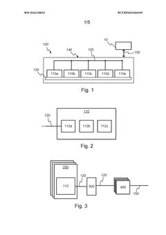
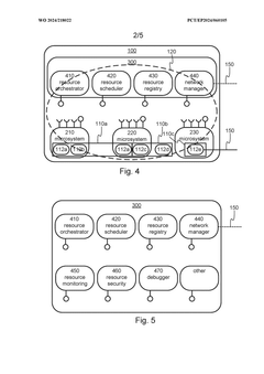
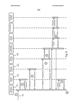
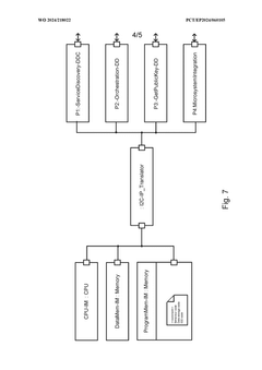
- A chiplet arrangement with a control plane that orchestrates microsystems and microservices, utilizing a resource orchestrator, network manager, and resource scheduler to dynamically instantiate and manage hardware resources based on availability and utilization, enabling optimized resource utilization, scalability, and reduced power consumption.
Method of executing programmable atomic unit resources within a multi-process system
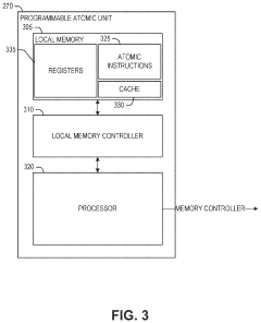
PatentActiveUS12020062B2
Innovation
- A method is disclosed that involves determining a unique identifier for a programmable atomic transaction within a process, using a mapping table to generate a system-wide identifier, and issuing requests to a memory controller to perform the transaction, allowing for efficient execution and response handling through a programmable atomic unit.
Chiplet Ecosystem
The chiplet ecosystem has rapidly evolved to become a critical component of modern semiconductor design and manufacturing. This ecosystem encompasses a wide range of players, technologies, and standards that collectively enable the development and production of chiplet-based systems. At its core, the ecosystem is built around the concept of disaggregating complex system-on-chip (SoC) designs into smaller, more manageable chiplets that can be mixed and matched to create customized solutions.
Key players in the chiplet ecosystem include semiconductor manufacturers, intellectual property (IP) providers, electronic design automation (EDA) tool vendors, and packaging companies. Major semiconductor companies such as Intel, AMD, and TSMC have invested heavily in chiplet technologies, driving innovation and standardization efforts. IP providers play a crucial role by offering pre-designed and verified chiplet components that can be integrated into larger systems, reducing development time and costs.
The ecosystem is supported by a growing set of standards and interfaces that facilitate interoperability between chiplets from different vendors. The Advanced Interface Bus (AIB) and Universal Chiplet Interconnect Express (UCIe) are examples of emerging standards that aim to create a common language for chiplet communication. These standards are essential for enabling a truly open and modular chiplet ecosystem.
Packaging technologies are another critical aspect of the chiplet ecosystem. Advanced packaging techniques such as 2.5D and 3D integration allow for the efficient combination of multiple chiplets into a single package. Companies specializing in advanced packaging, like ASE Group and Amkor Technology, are key enablers of chiplet-based designs.
The chiplet ecosystem also includes a robust supply chain for materials and manufacturing equipment. Specialized materials for interposers, substrates, and die-to-die interconnects are essential for realizing the full potential of chiplet designs. Equipment manufacturers are developing new tools and processes to support the unique requirements of chiplet assembly and testing.
As the ecosystem matures, we are seeing the emergence of chiplet marketplaces and design libraries. These platforms aim to simplify the process of sourcing and integrating chiplets from multiple vendors, further accelerating the adoption of chiplet-based designs across various industries.
The continued growth and development of the chiplet ecosystem are driving innovation in areas such as high-performance computing, artificial intelligence, and edge computing. As the ecosystem expands, it is enabling new business models and design approaches that promise to reshape the semiconductor industry landscape in the coming years.
Chiplet Standards
The evolution of chiplet design has necessitated the development of robust standards to ensure interoperability and facilitate widespread adoption. These standards play a crucial role in defining the interfaces, protocols, and packaging technologies that enable chiplets from different manufacturers to work seamlessly together.
One of the most significant standards in the chiplet ecosystem is the Universal Chiplet Interconnect Express (UCIe). Developed by a consortium of industry leaders, UCIe provides a standardized die-to-die interconnect that allows for high-bandwidth, low-latency communication between chiplets. This standard encompasses both the physical layer and the protocol layer, ensuring compatibility across different chiplet designs and manufacturers.
Another important standard is the Advanced Interface Bus (AIB), which was initially developed by Intel and later released as an open standard. AIB defines a high-speed chip-to-chip interface that supports both die-to-die and package-to-package connections. It offers flexibility in terms of bandwidth and power consumption, making it suitable for a wide range of applications.
The Open Compute Project (OCP) has also contributed to chiplet standardization efforts through its Open Domain-Specific Architecture (ODSA) subproject. The ODSA aims to create an open chiplet ecosystem by defining standards for chiplet interfaces, packaging, and testing. This initiative has led to the development of the Bunch of Wires (BoW) interface, a simple and cost-effective chiplet interconnect standard.
In addition to interconnect standards, packaging standards play a crucial role in chiplet integration. The Joint Electron Device Engineering Council (JEDEC) has developed standards for advanced packaging technologies, such as the JEP30 guideline for 2.5D and 3D multi-die interconnect bridge packaging. These standards ensure consistency in packaging methodologies and facilitate the integration of chiplets from different sources.
As chiplet technology continues to evolve, new standards are emerging to address specific challenges. For instance, the Compute Express Link (CXL) consortium is working on extending its high-speed interconnect standard to support chiplet-to-chiplet communication, potentially enabling more efficient and flexible system designs.
The development and adoption of these standards have been instrumental in driving the chiplet ecosystem forward. They provide a common framework for manufacturers, reduce design complexity, and enable the creation of more diverse and specialized chip solutions. As the chiplet approach gains momentum, ongoing collaboration between industry players to refine and expand these standards will be crucial for realizing the full potential of disaggregated chip design.
Unlock deeper insights with Patsnap Eureka Quick Research — get a full tech report to explore trends and direct your research. Try now!
Generate Your Research Report Instantly with AI Agent
Supercharge your innovation with Patsnap Eureka AI Agent Platform!