Chiplet Systems: The Future of Digital Integration and Expansion
JUL 16, 20259 MIN READ
Generate Your Research Report Instantly with AI Agent
Patsnap Eureka helps you evaluate technical feasibility & market potential.
Chiplet Evolution and Objectives
Chiplet technology has emerged as a revolutionary approach in the semiconductor industry, addressing the challenges of traditional monolithic chip design. The evolution of chiplets can be traced back to the early 2010s when the limitations of Moore's Law became increasingly apparent. As transistor scaling slowed down, chip designers sought alternative methods to improve performance and functionality while managing costs and power consumption.
The primary objective of chiplet technology is to enable the integration of multiple smaller dies, or "chiplets," onto a single package. This approach allows for the combination of different process nodes, intellectual property (IP) blocks, and specialized functions within a single system. By breaking down complex chip designs into smaller, more manageable components, chiplets offer increased flexibility, improved yield, and reduced manufacturing costs.
One of the key drivers behind chiplet adoption is the need for heterogeneous integration. As different components of a system-on-chip (SoC) require varying levels of performance and power efficiency, chiplets allow for the optimal selection of process nodes for each function. This modular approach enables designers to mix and match chiplets from different vendors, fostering innovation and competition in the semiconductor ecosystem.
The evolution of chiplet technology has been marked by several significant milestones. In 2017, AMD introduced its Infinity Fabric interconnect, which allowed for the efficient communication between multiple chiplets in its Zen-based processors. This breakthrough demonstrated the viability of chiplet-based designs in high-performance computing applications. Subsequently, other major players in the industry, including Intel and TSMC, have embraced chiplet technology and developed their own interconnect solutions.
As chiplet technology continues to mature, industry standards are being developed to ensure interoperability and facilitate broader adoption. The Universal Chiplet Interconnect Express (UCIe) consortium, formed in 2022, aims to establish a common interconnect standard for chiplets, enabling seamless integration across different vendors and technologies.
Looking ahead, the objectives of chiplet technology extend beyond performance improvements and cost reduction. Future developments aim to enhance power efficiency, reduce latency in inter-chiplet communication, and expand the range of applications for chiplet-based systems. Additionally, there is a growing focus on developing advanced packaging technologies to support more complex chiplet configurations and improve thermal management.
Market Demand Analysis for Chiplet Systems
The market demand for Chiplet Systems is experiencing a significant surge, driven by the increasing complexity and performance requirements of modern computing applications. As traditional monolithic chip designs approach their physical and economic limits, the industry is rapidly shifting towards modular and scalable chiplet-based architectures. This transition is fueled by the growing need for high-performance, energy-efficient, and cost-effective solutions across various sectors, including data centers, artificial intelligence, edge computing, and 5G infrastructure.
The global semiconductor market, which forms the foundation for chiplet systems, is projected to reach substantial growth in the coming years. This growth is largely attributed to the rising demand for advanced computing solutions in emerging technologies such as autonomous vehicles, Internet of Things (IoT) devices, and next-generation mobile networks. Chiplet systems are particularly well-positioned to address these market needs by offering improved performance, reduced power consumption, and enhanced scalability compared to traditional monolithic designs.
In the data center and cloud computing segment, the demand for chiplet systems is driven by the need for more powerful and efficient processors to handle the exponential growth in data processing and storage requirements. Major cloud service providers and enterprise customers are increasingly adopting chiplet-based solutions to optimize their infrastructure and reduce operational costs. The ability of chiplet systems to mix and match different process nodes and IP blocks allows for more customized and efficient designs, catering to the specific needs of diverse workloads.
The artificial intelligence and machine learning sector represents another significant market opportunity for chiplet systems. As AI models continue to grow in size and complexity, there is a pressing need for more powerful and specialized computing architectures. Chiplet-based designs enable the integration of diverse components, such as high-performance CPUs, GPUs, and dedicated AI accelerators, on a single package. This flexibility allows for the creation of highly optimized AI systems that can deliver superior performance and energy efficiency.
In the consumer electronics market, chiplet systems are gaining traction due to their ability to enable more powerful and feature-rich devices while maintaining reasonable power consumption and form factors. Smartphones, tablets, and other portable devices can benefit from the modular nature of chiplets, allowing manufacturers to quickly adapt to changing market demands and technological advancements.
The automotive industry is also emerging as a key market for chiplet systems, driven by the increasing electrification and automation of vehicles. Advanced driver assistance systems (ADAS) and autonomous driving technologies require sophisticated computing platforms that can process vast amounts of sensor data in real-time. Chiplet-based solutions offer the necessary performance and flexibility to meet these demanding requirements while adhering to the strict reliability and safety standards of the automotive sector.
As the market demand for chiplet systems continues to grow, industry collaborations and standardization efforts are gaining momentum. These initiatives aim to establish common interfaces and protocols, facilitating interoperability between chiplets from different vendors and accelerating the adoption of chiplet-based architectures across various industries.
Chiplet Technology Landscape and Challenges
Chiplet technology has emerged as a revolutionary approach in the semiconductor industry, addressing the challenges of traditional monolithic chip designs. The current landscape of chiplet technology is characterized by rapid advancements and growing adoption across various sectors. However, several significant challenges persist in the development and implementation of chiplet systems.
One of the primary challenges in chiplet technology is the standardization of interfaces. As chiplets from different manufacturers need to communicate seamlessly, the lack of universal standards for interconnects and protocols poses a significant hurdle. Industry consortia like ODSA (Open Domain-Specific Architecture) and UCIe (Universal Chiplet Interconnect Express) are working towards establishing common standards, but widespread adoption remains a work in progress.
Another critical challenge is the complexity of system integration. Chiplet-based designs require sophisticated packaging technologies, such as advanced 2.5D and 3D integration methods. These packaging techniques demand high precision and introduce new thermal management and signal integrity issues. Overcoming these integration challenges is crucial for realizing the full potential of chiplet systems.
Power management and distribution across multiple chiplets present another set of challenges. Efficiently delivering power to various components while managing heat dissipation becomes more complex in a disaggregated system. This requires innovative power delivery network designs and thermal solutions tailored for chiplet architectures.
Testing and validation of chiplet-based systems also pose unique challenges. Traditional testing methods may not be sufficient for ensuring the reliability and performance of interconnected chiplets. Developing new testing methodologies and tools specific to chiplet architectures is essential for quality assurance and yield improvement.
The economic aspects of chiplet technology present both opportunities and challenges. While chiplets offer the potential for cost reduction through mix-and-match flexibility and improved yield, the initial investment in design and manufacturing infrastructure can be substantial. Balancing these economic factors is crucial for widespread adoption of chiplet technology.
Lastly, the intellectual property (IP) landscape surrounding chiplet technology is complex. As chiplet designs often involve components from multiple vendors, managing IP rights and ensuring compatibility between different chiplets can be challenging. This necessitates new business models and collaboration frameworks within the semiconductor industry.
In conclusion, while chiplet technology offers promising solutions to the limitations of traditional chip design, it also brings forth a new set of challenges. Addressing these challenges requires concerted efforts from industry players, standardization bodies, and research institutions to fully realize the potential of chiplet systems as the future of digital integration and expansion.
Current Chiplet Integration Solutions
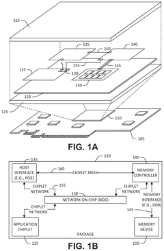
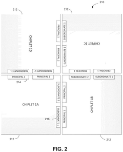
01 Chiplet interconnection and integration
Chiplet systems involve the integration of multiple smaller chips (chiplets) into a single package. This approach focuses on developing efficient interconnection technologies and integration methods to combine chiplets with different functionalities, improving overall system performance and flexibility.- Chiplet interconnection and integration: Chiplet systems involve the integration of multiple smaller chips (chiplets) into a single package. This approach focuses on developing efficient interconnection technologies and integration methods to combine chiplets with different functionalities, improving overall system performance and flexibility.
- Digital signal processing in chiplet systems: Chiplet-based systems incorporate advanced digital signal processing techniques to manage data flow between chiplets, optimize communication protocols, and enhance overall system efficiency. This includes implementing specialized algorithms and hardware accelerators for signal processing tasks within the chiplet architecture.
- Power management and thermal optimization: Effective power management and thermal optimization are crucial in chiplet systems. This involves developing intelligent power distribution schemes, implementing dynamic voltage and frequency scaling, and designing efficient cooling solutions to maintain optimal performance while minimizing energy consumption.
- Chiplet-based AI and machine learning acceleration: Chiplet architectures are being leveraged to create specialized AI and machine learning accelerators. This involves integrating dedicated neural processing units, tensor cores, and other AI-specific hardware within the chiplet ecosystem to enhance performance in AI workloads.
- Packaging and 3D integration technologies: Advanced packaging and 3D integration technologies play a crucial role in chiplet systems. This includes developing innovative interposer designs, through-silicon vias (TSVs), and die-to-die bonding techniques to enable high-density integration of chiplets in three-dimensional configurations.
02 Digital signal processing in chiplet systems
Digital signal processing techniques are crucial in chiplet systems for managing data flow between different chiplets. This includes implementing advanced algorithms for signal conditioning, synchronization, and error correction to ensure reliable communication and optimal performance across the integrated chiplets.Expand Specific Solutions03 Power management and thermal considerations
Effective power management and thermal control are essential in chiplet systems due to the high-density integration of multiple components. This involves developing sophisticated power distribution networks, implementing dynamic voltage and frequency scaling, and designing efficient cooling solutions to maintain system stability and performance.Expand Specific Solutions04 Packaging and 3D integration technologies
Advanced packaging and 3D integration technologies play a crucial role in chiplet system design. This includes developing novel interposer technologies, through-silicon vias (TSVs), and die-to-die bonding techniques to achieve high-density integration while maintaining signal integrity and thermal management.Expand Specific Solutions05 Design automation and optimization for chiplet systems
Developing specialized electronic design automation (EDA) tools and methodologies is crucial for optimizing chiplet-based system design. This includes creating new algorithms for chiplet placement, routing, and system-level optimization to achieve the best balance between performance, power consumption, and cost in complex multi-chiplet architectures.Expand Specific Solutions
Key Players in Chiplet Ecosystem
The chiplet systems market is in a growth phase, driven by increasing demand for high-performance computing and AI applications. The market size is expanding rapidly, with major players like Intel, AMD, and TSMC investing heavily in chiplet technology. The competitive landscape is characterized by a mix of established semiconductor giants and innovative startups. Technologically, chiplet systems are maturing, with companies like Micron, Intel, and AMD leading in advanced packaging and integration techniques. However, challenges remain in standardization and interoperability. The involvement of research institutions such as Shandong University and the Institute of Microelectronics of Chinese Academy of Sciences indicates ongoing development in this field, suggesting potential for further technological advancements and market expansion.
Intel Corp.
Technical Solution: Intel's Foveros 3D packaging technology is a key innovation in chiplet systems. It allows for vertical stacking of multiple chiplets, enabling higher performance and lower power consumption. Intel's Ponte Vecchio GPU, built on Foveros, incorporates over 40 chiplets in a single package[1]. The company has also introduced its next-generation Foveros Direct technology, which promises to reduce the interconnect pitch to 10 microns, further enhancing chiplet integration[2]. Intel's EMIB (Embedded Multi-die Interconnect Bridge) technology complements Foveros by providing high-bandwidth connections between chiplets in a 2.5D arrangement[3].
Strengths: Advanced 3D packaging capabilities, high integration density, and flexibility in chip design. Weaknesses: Complex manufacturing process, potential thermal management challenges in densely packed 3D structures.
Advanced Micro Devices, Inc.
Technical Solution: AMD has pioneered the use of chiplets in consumer processors with its Zen architecture. The company's Infinity Fabric interconnect technology allows for the efficient connection of multiple chiplets within a single package. AMD's EPYC server processors utilize up to eight CPU chiplets connected to a central I/O die[4]. This approach has enabled AMD to scale its processor designs efficiently, offering high core counts and performance. The company has also introduced 3D V-Cache technology, which stacks additional cache memory on top of CPU chiplets, significantly increasing cache capacity and improving performance in certain workloads[5].
Strengths: Scalable architecture, cost-effective manufacturing by using smaller chiplets, and ability to mix-and-match chiplets for different product configurations. Weaknesses: Potential latency issues between chiplets, reliance on advanced packaging technologies.
Core Innovations in Chiplet Technology
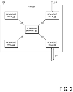
Technologies for a unified test and debug architecture
PatentPendingUS20240329129A1
Innovation
- A unified test and debug architecture is implemented using an external hardware debug interface that supports multiple protocols, including UCIe, JTAG, I2C, and PCIe, allowing debug messages to be sent and routed through a package with multiple chiplets, enabling interoperable debug/test solutions and facilitating infield debugging.
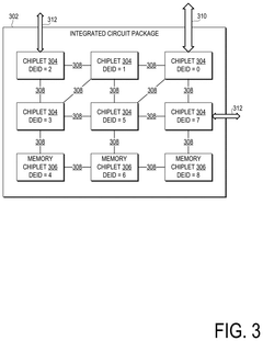
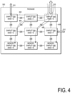
Edge interface placements to enable chiplet rotation into multi-chiplet cluster
PatentPendingUS20240332257A1
Innovation
- The implementation of a chiplet architecture that uses a network-on-chip (NOC) with a chiplet protocol interface (CPI) to facilitate high-speed, flexible inter-chiplet communication, combined with a tightly packed matrix arrangement of chiplets and I/O micro-bumps for close-coupled interconnects, allowing for proper alignment and minimal footprint.
Standardization Efforts in Chiplet Industry
Standardization efforts in the chiplet industry have become increasingly crucial as the technology gains momentum. These initiatives aim to establish common protocols, interfaces, and design methodologies to ensure interoperability and facilitate widespread adoption of chiplet-based systems.
One of the most prominent standardization efforts is the Universal Chiplet Interconnect Express (UCIe) consortium. Launched in 2022, UCIe brings together industry leaders such as Intel, AMD, Arm, TSMC, and Samsung to develop an open specification for die-to-die interconnects. The UCIe 1.0 specification, released in March 2022, defines the physical and logical layers for chiplet-to-chiplet communication, enabling a more modular approach to chip design.
Another significant standardization initiative is the Open Compute Project's (OCP) Chiplet Design Exchange (CDX) format. CDX aims to create a standardized way of describing chiplet designs, facilitating easier integration and collaboration between different chiplet providers. This format is crucial for enabling a more diverse and competitive chiplet ecosystem.
The JEDEC Solid State Technology Association has also been active in chiplet standardization. Their JC-63 Committee for Chiplets is working on developing standards for chiplet-based memory systems, addressing the growing need for high-bandwidth, low-latency memory solutions in advanced computing applications.
In addition to these industry-wide efforts, several companies are developing their own chiplet standards. For instance, AMD's Infinity Fabric and Intel's Advanced Interface Bus (AIB) are proprietary interconnect technologies that have been made available for broader use, contributing to the overall standardization landscape.
The importance of these standardization efforts cannot be overstated. They are crucial for reducing design complexity, lowering costs, and accelerating time-to-market for chiplet-based systems. By establishing common interfaces and protocols, these standards enable chiplets from different vendors to work together seamlessly, fostering innovation and competition in the semiconductor industry.
However, challenges remain in achieving full standardization. The rapid pace of technological advancement in the chiplet space means that standards must be flexible and adaptable to accommodate future innovations. Additionally, balancing the needs of different stakeholders and ensuring widespread adoption of standards across the industry requires ongoing collaboration and compromise.
Thermal Management in Chiplet Systems
Thermal management is a critical aspect of chiplet systems, as the integration of multiple dies on a single package introduces unique challenges in heat dissipation and temperature control. The compact nature of chiplet designs leads to increased power density, which can result in localized hotspots and overall thermal issues that may impact system performance and reliability.
One of the primary thermal management strategies in chiplet systems involves the use of advanced packaging technologies. These include the implementation of through-silicon vias (TSVs) and microbumps, which not only facilitate electrical connections but also aid in heat transfer between dies and the package substrate. Additionally, the use of thermal interface materials (TIMs) with high thermal conductivity is crucial for efficient heat dissipation from the chiplets to the heat spreader or heat sink.
The design of the package substrate itself plays a significant role in thermal management. Substrates with embedded cooling channels or integrated heat spreaders can help distribute heat more evenly across the package, reducing the risk of hotspots. Some advanced designs incorporate liquid cooling directly into the substrate, allowing for more efficient heat removal from high-power chiplets.
Active cooling solutions are often necessary to maintain optimal operating temperatures in chiplet systems. These may include traditional air cooling with high-performance heatsinks and fans, as well as more advanced liquid cooling systems. In some cases, two-phase cooling solutions, such as vapor chambers or heat pipes, are employed to handle the high heat fluxes generated by densely packed chiplets.
Thermal modeling and simulation tools are essential in the design process of chiplet systems. These tools allow engineers to predict thermal behavior, identify potential hotspots, and optimize the placement of chiplets and cooling solutions. Advanced thermal management techniques, such as dynamic thermal management (DTM) and adaptive voltage scaling, are also implemented to balance performance and power consumption based on real-time temperature monitoring.
As chiplet systems continue to evolve, emerging technologies are being explored to address thermal challenges. These include the use of novel materials with superior thermal properties, such as graphene-based heat spreaders or diamond-copper composites. Additionally, three-dimensional integrated circuits (3D ICs) with interlayer cooling are being researched to provide more effective heat removal in highly stacked chiplet configurations.
The future of thermal management in chiplet systems will likely involve a combination of innovative packaging technologies, advanced cooling solutions, and intelligent thermal management algorithms. As the demand for higher performance and more compact designs continues to grow, addressing thermal challenges will remain a critical factor in the success and widespread adoption of chiplet-based architectures.
Unlock deeper insights with Patsnap Eureka Quick Research — get a full tech report to explore trends and direct your research. Try now!
Generate Your Research Report Instantly with AI Agent
Supercharge your innovation with Patsnap Eureka AI Agent Platform!