Chiplet Technology and Its Implications for Cloud Computing
JUL 16, 20259 MIN READ
Generate Your Research Report Instantly with AI Agent
Patsnap Eureka helps you evaluate technical feasibility & market potential.
Chiplet Evolution and Objectives
Chiplet technology has emerged as a revolutionary approach in semiconductor design and manufacturing, marking a significant shift from traditional monolithic chip architectures. This evolution began in the early 2010s as a response to the slowing of Moore's Law and the increasing challenges in scaling transistor sizes. The primary objective of chiplet technology is to overcome the limitations of conventional chip design by disaggregating complex systems-on-chip (SoCs) into smaller, more manageable components.
The development of chiplet technology can be traced through several key milestones. Initially, the focus was on creating standardized interfaces for connecting different chiplets. This led to the development of protocols such as Intel's Advanced Interface Bus (AIB) and AMD's Infinity Fabric. These interfaces enabled the integration of heterogeneous components, allowing for more flexible and cost-effective chip designs.
As the technology progressed, the industry saw the introduction of 2.5D and 3D packaging techniques, which further enhanced the capabilities of chiplet-based designs. These advanced packaging methods allowed for higher bandwidth connections between chiplets and improved overall system performance. The adoption of through-silicon vias (TSVs) and silicon interposers played a crucial role in enabling these packaging innovations.
In recent years, the objectives of chiplet technology have expanded beyond mere performance improvements. There is now a strong focus on energy efficiency, as chiplets allow for more optimized power distribution and thermal management. Additionally, chiplet technology aims to reduce manufacturing costs by enabling the use of different process nodes for different components within a single package.
For cloud computing, chiplet technology presents several compelling objectives. Firstly, it allows for the creation of highly customized processors tailored to specific cloud workloads, potentially improving performance and energy efficiency in data centers. Secondly, chiplets offer the possibility of more rapid innovation cycles, as individual components can be upgraded without redesigning entire chips.
Looking forward, the evolution of chiplet technology is expected to continue with advancements in interconnect technologies, further miniaturization of components, and the development of more sophisticated design and integration tools. The ultimate goal is to create a "chiplet ecosystem" where standardized components from different manufacturers can be seamlessly integrated, fostering innovation and competition in the semiconductor industry.
Cloud Computing Market Demand
The cloud computing market has experienced exponential growth in recent years, driven by the increasing demand for scalable, flexible, and cost-effective IT infrastructure. As organizations across various sectors continue to digitize their operations and embrace cloud-native technologies, the need for more powerful and efficient cloud computing solutions has become paramount. This growing demand has created a fertile ground for innovative technologies like Chiplet to make significant impacts.
The global cloud computing market size was valued at $368.97 billion in 2021 and is projected to reach $1,554.94 billion by 2030, growing at a CAGR of 17.3% from 2022 to 2030. This robust growth is fueled by several factors, including the rapid adoption of remote work models, the proliferation of IoT devices, and the increasing implementation of artificial intelligence and machine learning technologies.
Within this expanding market, there is a notable shift towards more specialized and high-performance computing solutions. Enterprise customers are increasingly demanding cloud services that can handle complex workloads, such as big data analytics, AI model training, and real-time data processing. This trend aligns well with the potential benefits of Chiplet technology, which promises to deliver enhanced performance and efficiency in cloud computing environments.
The demand for edge computing capabilities is also on the rise, with the market expected to grow from $3.6 billion in 2020 to $15.7 billion by 2025. This growth presents another opportunity for Chiplet technology, as it can enable more powerful and energy-efficient edge devices, facilitating the processing of data closer to its source and reducing latency for time-sensitive applications.
Furthermore, sustainability has become a critical concern for cloud service providers and their customers. The global green technology and sustainability market size is projected to grow from $11.2 billion in 2020 to $36.6 billion by 2025. Chiplet technology's potential to improve energy efficiency in data centers aligns with this growing demand for more sustainable cloud computing solutions.
As the cloud computing market continues to evolve, there is an increasing emphasis on customization and specialization. Cloud service providers are looking for ways to differentiate their offerings and cater to specific industry needs. Chiplet technology's modular approach could enable more tailored and optimized cloud computing solutions, addressing the diverse requirements of different market segments.
In conclusion, the robust growth and evolving demands of the cloud computing market create a favorable environment for the adoption and development of Chiplet technology. Its potential to enhance performance, improve energy efficiency, and enable more customized solutions aligns well with the current market trends and future projections in the cloud computing industry.
Chiplet Tech Status and Hurdles
Chiplet technology has made significant strides in recent years, revolutionizing the semiconductor industry and cloud computing landscape. However, despite its promising potential, several challenges and hurdles remain in its widespread adoption and implementation.
One of the primary challenges facing chiplet technology is the complexity of integration. As chiplets are essentially smaller, modular components of a larger system-on-chip (SoC), ensuring seamless communication and coordination between these individual units presents a significant technical hurdle. The development of efficient and standardized interfaces for chiplet-to-chiplet communication is crucial for optimal performance and scalability.
Another major obstacle is the need for advanced packaging technologies. Traditional packaging methods are often inadequate for the intricate requirements of chiplet-based designs. The industry is actively working on developing more sophisticated packaging solutions, such as 2.5D and 3D integration techniques, to address this challenge. However, these advanced packaging technologies are still evolving and come with their own set of manufacturing complexities and cost implications.
Thermal management poses yet another significant challenge in chiplet technology. As multiple chiplets are integrated into a single package, managing heat dissipation becomes increasingly complex. Efficient cooling solutions and thermal design considerations are critical to ensure optimal performance and reliability of chiplet-based systems, particularly in high-performance cloud computing environments.
The issue of yield and cost-effectiveness also presents a hurdle in chiplet adoption. While chiplets offer the potential for improved yields by allowing manufacturers to produce smaller, less complex dies, the overall manufacturing process can still be complex and costly. Balancing the benefits of modular design with the additional costs of integration and packaging remains an ongoing challenge for the industry.
Standardization is another key hurdle in the chiplet ecosystem. The lack of universal standards for chiplet design, interfaces, and integration can hinder interoperability and limit the potential for mix-and-match capabilities across different vendors. Industry-wide collaboration is necessary to establish common standards and protocols that will facilitate broader adoption and innovation in chiplet technology.
In terms of geographical distribution, chiplet technology development is primarily concentrated in regions with strong semiconductor industries, such as the United States, Taiwan, South Korea, and parts of Europe. However, as the technology gains traction, we are seeing increased interest and investment in chiplet research and development across other regions, including China and Japan.
Despite these challenges, the potential benefits of chiplet technology for cloud computing are driving continued innovation and investment in overcoming these hurdles. As the technology matures and solutions to these challenges emerge, we can expect to see wider adoption and more sophisticated applications of chiplets in cloud computing infrastructure and beyond.
Current Chiplet Solutions
01 Chiplet integration and packaging
Chiplet technology involves integrating multiple smaller chips (chiplets) into a single package. This approach allows for more flexible and efficient chip design, enabling the combination of different functionalities or process nodes within one package. Advanced packaging techniques are used to connect these chiplets, improving overall system performance and reducing costs.- Chiplet integration and packaging: Chiplet technology involves integrating multiple smaller chips (chiplets) into a single package. This approach allows for more flexible and cost-effective semiconductor design by combining different functional units or IP blocks. Advanced packaging techniques, such as 2.5D and 3D integration, are used to interconnect these chiplets, enabling higher performance and improved power efficiency in complex systems.
- Interconnect technologies for chiplets: Various interconnect technologies are crucial for chiplet-based designs. These include advanced interposer designs, through-silicon vias (TSVs), and high-bandwidth interfaces. Such technologies enable efficient communication between chiplets, reducing latency and power consumption while increasing overall system performance. The development of standardized interconnect protocols is also a key focus in chiplet technology.
- Thermal management in chiplet designs: Effective thermal management is critical in chiplet-based systems due to the high density of components. Innovative cooling solutions, such as integrated liquid cooling channels, advanced heat spreaders, and thermal interface materials, are being developed to address the thermal challenges associated with chiplet integration. These solutions aim to maintain optimal operating temperatures and ensure reliable performance.
- Design and verification tools for chiplets: Specialized design and verification tools are essential for chiplet-based architectures. These tools facilitate the design, simulation, and testing of complex multi-chiplet systems. They include advanced EDA software for chiplet floor planning, power analysis, and signal integrity verification. Additionally, tools for managing the integration of heterogeneous chiplets and ensuring system-level compatibility are being developed.
- AI and machine learning applications in chiplet technology: Artificial intelligence and machine learning are increasingly being applied to chiplet technology. This includes AI-driven design optimization for chiplet layouts, predictive performance modeling, and automated testing procedures. Machine learning algorithms are also being used to enhance the efficiency of chiplet-to-chiplet communication and to optimize power management in complex multi-chiplet systems.
02 Interconnect technologies for chiplets
Various interconnect technologies are employed to facilitate communication between chiplets and with the package substrate. These may include advanced through-silicon vias (TSVs), micro-bumps, and high-bandwidth interfaces. The choice of interconnect technology impacts the overall performance, power efficiency, and thermal management of the chiplet-based system.Expand Specific Solutions03 Thermal management in chiplet designs
Effective thermal management is crucial in chiplet-based systems due to the high density of components. Innovative cooling solutions, such as integrated liquid cooling or advanced heat spreaders, are developed to address thermal challenges. Proper thermal design ensures optimal performance and reliability of the chiplet assembly.Expand Specific Solutions04 Power distribution and management for chiplets
Efficient power distribution and management are essential in chiplet designs to ensure proper functioning of all components. This includes advanced power delivery networks, voltage regulation techniques, and power gating strategies. Optimizing power distribution helps maintain performance while minimizing energy consumption in chiplet-based systems.Expand Specific Solutions05 Testing and yield improvement for chiplet technology
Developing effective testing methodologies for chiplet-based systems is crucial for ensuring quality and reliability. This includes pre-integration testing of individual chiplets, as well as post-integration testing of the complete assembly. Advanced testing techniques and yield improvement strategies are implemented to enhance the overall manufacturability and cost-effectiveness of chiplet technology.Expand Specific Solutions
Key Chiplet Industry Players
The chiplet technology market for cloud computing is in its early growth stage, with significant potential for expansion. The market size is expected to grow rapidly as major players invest heavily in research and development. While the technology is still evolving, it is gaining maturity with companies like Intel, AMD, and Huawei leading the way. These firms are developing advanced chiplet designs to address the increasing demands of cloud computing. Other key players such as Micron, ZTE, and Baidu are also contributing to the ecosystem, focusing on memory, networking, and AI applications respectively. The competitive landscape is dynamic, with both established semiconductor giants and innovative startups vying for market share in this promising field.
Huawei Technologies Co., Ltd.
Technical Solution: Huawei has developed its own chiplet technology, focusing on high-performance computing and cloud applications. Their approach involves a "chiplet-based heterogeneous integration" strategy, allowing for the combination of diverse computing units optimized for specific tasks[7]. Huawei's Kunpeng series of ARM-based server processors utilize chiplet technology to achieve high core counts and performance efficiency. The company has also invested in advanced packaging technologies, including fan-out wafer-level packaging (FOWLP) and through-silicon vias (TSVs), to enable more sophisticated chiplet integrations[8]. Huawei's chiplet designs aim to provide flexible, scalable solutions for various cloud computing scenarios, from edge computing to large-scale data centers.
Strengths: Heterogeneous integration capabilities, ARM-based efficiency, and advanced packaging technologies. Weaknesses: Potential geopolitical challenges affecting supply chain and market access.
Intel Corp.
Technical Solution: Intel's Chiplet technology, known as "Foveros," utilizes 3D packaging to stack multiple chiplets vertically. This approach allows for the integration of diverse IP blocks and process nodes in a single package. Intel's Meteor Lake processors, slated for cloud computing applications, employ Foveros technology to combine compute, graphics, and AI tiles[1]. The company has also introduced its "Embedded Multi-die Interconnect Bridge" (EMIB) technology, which enables high-bandwidth connections between chiplets in a 2.5D configuration, crucial for data-intensive cloud computing tasks[2]. Intel's chiplets are designed to optimize performance per watt, a critical factor in cloud data centers[3].
Strengths: Advanced 3D stacking capabilities, high-bandwidth inter-chiplet connections, and flexibility in combining different process nodes. Weaknesses: Potential thermal management challenges in dense 3D stacks and higher manufacturing complexity.
Core Chiplet Innovations
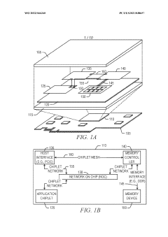
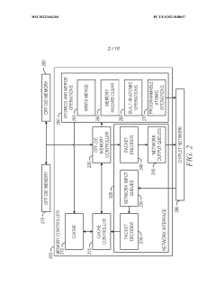
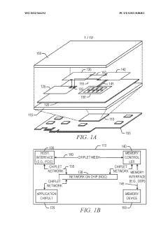
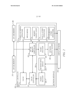
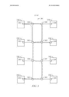
Mapping high-speed, point-to-point interface channels to packet virtual channels
PatentWO2022046260A1
Innovation
- Mapping AXI channels to packet virtual channels allows for independent flow control, enabling any AXI channel to be processed without blocking due to another channel's stall by converting data into a packet format and using virtual channels for transmission.
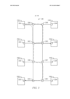
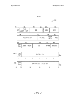
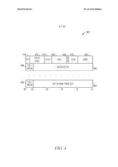
Combined write enable mask and credit return field
PatentWO2022046253A1
Innovation
- A combined write enable mask and credit return field is introduced in data packets, allowing the field to function as either a write enable mask or credit return field based on a selection value, reducing the need for separate packets and optimizing packet size.
Chiplet Standardization
Chiplet standardization is a critical aspect of the evolving chiplet technology landscape, particularly in its implications for cloud computing. As the industry moves towards disaggregated chip designs, the need for common standards and protocols becomes increasingly apparent.
The primary goal of chiplet standardization is to enable interoperability between chiplets from different manufacturers. This is crucial for creating a robust ecosystem where cloud service providers can mix and match chiplets to build customized, high-performance systems. Several industry consortia and organizations are working towards developing these standards, with notable efforts including the Universal Chiplet Interconnect Express (UCIe) and the Open Compute Project's Open Domain-Specific Architecture (ODSA).
UCIe, backed by major players like Intel, AMD, and TSMC, aims to establish a unified die-to-die interconnect standard. This standard covers both the physical layer and the protocol layer, ensuring seamless communication between chiplets. The adoption of UCIe could significantly reduce design complexity and time-to-market for cloud computing hardware.
Another key area of standardization is the development of common interfaces for chiplets. These interfaces define how chiplets communicate with each other and with the package substrate. Standardized interfaces can greatly simplify system integration and enable more flexible and scalable cloud computing architectures.
Power management and thermal considerations are also crucial aspects of chiplet standardization. As cloud data centers strive for greater energy efficiency, standardized approaches to power distribution and heat dissipation across multiple chiplets become essential. This includes developing common protocols for dynamic power management and thermal monitoring across chiplet-based systems.
Standardization efforts also extend to packaging technologies. Advanced packaging techniques, such as 2.5D and 3D integration, are integral to chiplet-based designs. Establishing standards for these packaging methods can help ensure compatibility and reliability across different chiplet implementations in cloud computing environments.
Data security and integrity are paramount in cloud computing, and chiplet standardization must address these concerns. This includes developing standard protocols for secure communication between chiplets and implementing hardware-level security features that can be consistently applied across different chiplet designs.
As chiplet technology continues to evolve, standardization efforts will need to keep pace with emerging trends and requirements in cloud computing. This may include standards for integrating AI accelerators, optimizing memory interfaces, and supporting new networking protocols. The success of these standardization efforts will play a crucial role in shaping the future of cloud computing infrastructure.
Energy Efficiency Impact
Chiplet technology has significant implications for energy efficiency in cloud computing environments. By enabling the disaggregation of large monolithic chips into smaller, more specialized components, chiplets offer several advantages that contribute to improved energy efficiency.
One of the primary benefits of chiplet technology is the ability to optimize power consumption for specific workloads. In cloud computing scenarios, where diverse applications and services run concurrently, chiplets allow for more granular control over power allocation. This means that different components can be powered on or off as needed, reducing overall energy consumption when certain functions are not in use.
Furthermore, chiplets enable the use of heterogeneous integration, combining different process nodes and specialized components on a single package. This approach allows for the incorporation of high-performance cores for compute-intensive tasks alongside more energy-efficient cores for less demanding operations. In cloud data centers, this translates to improved performance-per-watt metrics, as workloads can be dynamically assigned to the most appropriate processing units.
The modular nature of chiplets also contributes to better thermal management. By distributing heat-generating components across a larger surface area, chiplet designs can more effectively dissipate heat, reducing the need for energy-intensive cooling systems. This is particularly crucial in data center environments, where cooling costs represent a significant portion of overall energy expenditure.
Additionally, chiplet technology allows for more efficient use of silicon wafers during manufacturing. By producing smaller dies, manufacturers can achieve higher yields and reduce waste, indirectly contributing to energy savings in the production process. This efficiency in manufacturing also leads to cost reductions, which can be reinvested in further energy-saving innovations for cloud infrastructure.
The impact of chiplets on interconnect efficiency is another crucial factor in energy savings. By optimizing the communication pathways between different functional units, chiplet designs can reduce signal transmission distances and power consumption associated with data movement. In cloud computing, where vast amounts of data are constantly being processed and transferred, these improvements in interconnect efficiency can lead to substantial energy savings at scale.
Looking ahead, the energy efficiency benefits of chiplet technology are likely to become even more pronounced as cloud computing continues to grow. As data centers face increasing pressure to reduce their carbon footprint, the adoption of chiplet-based systems presents a promising avenue for achieving sustainability goals while meeting the ever-growing demand for computing power.
Unlock deeper insights with Patsnap Eureka Quick Research — get a full tech report to explore trends and direct your research. Try now!
Generate Your Research Report Instantly with AI Agent
Supercharge your innovation with Patsnap Eureka AI Agent Platform!