

Cryogenic Electronics: Advances in Quantum Sensor Technologies
SEP 29, 20259 MIN READ
Generate Your Research Report Instantly with AI Agent
PatSnap Eureka helps you evaluate technical feasibility & market potential.
Cryogenic Electronics Background and Objectives
Cryogenic electronics represents a frontier domain at the intersection of quantum physics, materials science, and electronic engineering, focusing on the behavior and application of electronic systems at extremely low temperatures. The field traces its origins to the early 20th century with the discovery of superconductivity by Heike Kamerlingh Onnes in 1911, which revealed that certain materials can conduct electricity with zero resistance when cooled near absolute zero.
The evolution of cryogenic electronics has been marked by significant milestones, including the development of Josephson junctions in the 1960s, the discovery of high-temperature superconductors in the 1980s, and recent breakthroughs in quantum computing and sensing technologies. This progression has transformed cryogenic electronics from a purely theoretical curiosity to a practical technology with diverse applications.
Current technological trends in cryogenic electronics are primarily driven by the quantum information revolution, with particular emphasis on quantum sensors that leverage quantum mechanical properties for unprecedented measurement precision. These sensors exploit phenomena such as quantum coherence, entanglement, and superposition to detect minute changes in physical parameters including magnetic fields, electric fields, and gravitational waves.
The primary objective of advancing quantum sensor technologies within cryogenic electronics is to develop systems capable of operating reliably at temperatures below 4 Kelvin while achieving quantum-limited sensitivity. This involves overcoming significant engineering challenges related to thermal management, signal integrity, and material properties at extreme temperatures.
Specific technical goals include the development of more energy-efficient cooling systems, integration of quantum sensors with conventional electronics, improvement of quantum coherence times, and miniaturization of cryogenic components for practical deployment. Additionally, there is a focus on creating standardized interfaces between cryogenic quantum systems and room-temperature control electronics.
The field aims to bridge fundamental quantum physics with practical engineering solutions, ultimately enabling transformative applications in areas such as medical imaging, geological surveying, navigation systems, and fundamental physics research. The convergence of quantum information science with cryogenic engineering presents unique opportunities for technological innovation.
Long-term objectives include the realization of scalable quantum sensor networks, development of portable cryogenic systems for field applications, and establishment of comprehensive design methodologies for cryogenic electronic circuits that can operate reliably in extreme environments while maintaining quantum performance advantages.
Market Analysis for Quantum Sensor Applications
The quantum sensor market is experiencing significant growth, driven by advancements in cryogenic electronics and quantum technologies. Current market valuations place the global quantum sensing market at approximately 400 million USD in 2023, with projections indicating growth to reach 1.2 billion USD by 2028, representing a compound annual growth rate (CAGR) of 24.6%. This remarkable expansion reflects the increasing recognition of quantum sensors' superior capabilities compared to conventional sensing technologies.
Healthcare and biomedical applications currently constitute the largest market segment, accounting for roughly 32% of quantum sensor deployments. The exceptional sensitivity of quantum sensors enables non-invasive medical imaging techniques such as improved Magnetic Resonance Imaging (MRI) and magnetoencephalography, offering unprecedented insights into biological processes at the molecular level.
Defense and security applications represent the fastest-growing segment with a CAGR of 29.3%. Military organizations and security agencies are investing heavily in quantum sensing technologies for enhanced navigation in GPS-denied environments, submarine detection, and advanced radar systems that can identify stealth aircraft.
Geographically, North America leads the market with approximately 42% share, followed by Europe at 28% and Asia-Pacific at 22%. However, the Asia-Pacific region is expected to witness the highest growth rate over the next five years due to substantial investments by China, Japan, and South Korea in quantum technologies.
Key demand drivers include the miniaturization of quantum sensors, which is expanding their applicability in consumer electronics and IoT devices. Additionally, the integration of quantum sensors with AI and machine learning algorithms is creating new use cases in predictive maintenance and structural health monitoring across industrial sectors.
Market challenges primarily revolve around the high costs associated with cryogenic cooling systems required for many quantum sensors. Current systems can cost between 50,000 to 200,000 USD, limiting widespread adoption. However, recent innovations in high-temperature superconducting materials and more efficient cooling technologies are gradually addressing this barrier.
Customer segments show varying adoption patterns, with large research institutions and government agencies currently dominating purchases. However, commercial adoption is accelerating in industries such as automotive (for autonomous vehicle navigation), telecommunications (for precise timing), and financial services (for secure quantum-encrypted communications).
The market is also witnessing increased venture capital interest, with quantum sensing startups raising over 300 million USD in funding during 2022, a 45% increase from the previous year, indicating strong investor confidence in the commercial potential of these technologies.
Current State and Challenges in Cryogenic Electronics
Cryogenic electronics has witnessed significant advancements globally, with quantum sensor technologies emerging as a frontier application domain. Currently, the field operates primarily at temperatures below 4 Kelvin, with cutting-edge quantum applications requiring even lower temperatures approaching millikelvin ranges. This extreme operating environment presents unique challenges for electronic components and systems.
The current technological landscape is characterized by specialized superconducting materials and devices, including Josephson junctions, SQUIDs (Superconducting Quantum Interference Devices), and various quantum-limited amplifiers. These technologies have enabled unprecedented measurement sensitivity in applications ranging from quantum computing to dark matter detection. Recent breakthroughs in materials science have yielded superconducting thin films with improved coherence properties and reduced loss tangents.
Despite these advances, significant technical challenges persist. Power dissipation remains a critical constraint, as cooling capacity at cryogenic temperatures is extremely limited—typically measured in microwatts at millikelvin temperatures. This severely restricts the complexity and scale of electronic systems that can operate in these environments. Thermal management therefore represents one of the most formidable obstacles to scaling cryogenic electronic systems.
Integration challenges also abound, particularly at the interface between room-temperature control electronics and cryogenic quantum devices. Signal integrity degradation, impedance matching issues, and thermal loading through interconnects all complicate system design. The development of cryogenic CMOS technologies has progressed, but still lags significantly behind room-temperature counterparts in terms of performance, reliability, and integration density.
Material limitations constitute another major hurdle. Many conventional electronic materials exhibit dramatically different properties at cryogenic temperatures, including altered carrier mobility, modified band structures, and frozen-out dopants. This necessitates extensive recharacterization and often complete redesign of electronic components for cryogenic operation.
Geographically, research leadership in cryogenic electronics is concentrated in North America, Europe, and parts of Asia. The United States maintains prominence through national laboratories and university research centers, while European efforts are coordinated through quantum technology initiatives. Japan has historically maintained strength in superconducting electronics, while China is rapidly expanding its capabilities in this domain.
Commercial development remains limited to specialized providers, with few large-scale industrial players fully committed to cryogenic electronics development. This creates a fragmented supply chain that further complicates technology advancement and standardization efforts. The specialized nature of cryogenic testing equipment and facilities also creates significant barriers to entry for new research groups and companies.
Current Cryogenic Cooling Solutions for Quantum Sensors
01 Superconducting quantum sensors for cryogenic applications
Superconducting materials are utilized in quantum sensors operating at cryogenic temperatures to achieve high sensitivity measurements. These sensors leverage quantum effects such as flux quantization and Josephson effects that emerge at extremely low temperatures. The superconducting circuits can detect minute magnetic fields, electromagnetic radiation, and other physical quantities with unprecedented precision, making them valuable for scientific research and advanced sensing applications.- Superconducting quantum sensors for cryogenic applications: Superconducting materials are utilized in quantum sensors operating at cryogenic temperatures to achieve high sensitivity and low noise. These sensors leverage quantum effects such as flux quantization and Josephson effects to detect extremely weak magnetic fields and electromagnetic signals. The superconducting circuits maintain quantum coherence at ultra-low temperatures, enabling precise measurements for applications in quantum computing, medical imaging, and fundamental physics research.
- Cryogenic cooling systems for quantum electronic devices: Specialized cooling systems are designed to maintain quantum electronic devices at extremely low temperatures required for their operation. These systems employ various cooling techniques including dilution refrigeration, pulse tube coolers, and liquid helium systems to achieve temperatures near absolute zero. The cooling infrastructure incorporates thermal isolation, vibration damping, and precise temperature control to maintain stable operating conditions for sensitive quantum sensors and superconducting circuits.
- SQUID-based quantum sensing technology: Superconducting Quantum Interference Devices (SQUIDs) are highly sensitive magnetometers operating at cryogenic temperatures that can detect extremely weak magnetic fields. These devices utilize quantum effects in superconducting loops containing Josephson junctions to achieve unprecedented sensitivity. SQUID-based sensors are applied in various fields including medical imaging (magnetoencephalography and magnetocardiography), geophysical surveys, materials characterization, and quantum information processing, where they can detect magnetic fields at the quantum limit.
- Integration of quantum sensors with cryogenic readout electronics: Advanced integration techniques enable the coupling of quantum sensors with specialized cryogenic readout electronics to minimize noise and signal degradation. These integrated systems incorporate low-power amplifiers, multiplexers, and signal processing circuits designed to operate at extremely low temperatures. The close integration of sensors and electronics reduces thermal loads, improves signal-to-noise ratios, and enables scalable quantum sensing arrays for applications in quantum computing, dark matter detection, and precision measurement systems.
- Quantum-limited detection systems for space and defense applications: Cryogenic quantum sensors are developed for space-based and defense applications requiring ultimate sensitivity and reliability in extreme environments. These systems incorporate radiation-hardened components, specialized packaging, and robust thermal management to withstand launch conditions and space environments. Applications include gravitational wave detection, Earth observation, deep space communications, and advanced surveillance systems where quantum-limited detection capabilities provide significant advantages over conventional technologies.
02 Cryogenic cooling systems for quantum electronic devices
Specialized cooling systems are essential for maintaining quantum electronic devices at the ultra-low temperatures required for their operation. These systems employ various refrigeration techniques including dilution refrigerators, pulse tube coolers, and liquid helium systems to reach temperatures near absolute zero. The cooling infrastructure is designed to minimize thermal noise and vibration while providing stable temperature environments necessary for quantum coherence in sensitive electronic components.Expand Specific Solutions03 Integration of quantum sensors with cryogenic readout electronics
The integration of quantum sensors with specialized cryogenic readout electronics addresses the challenge of signal processing at extremely low temperatures. These integrated systems include low-noise amplifiers, multiplexers, and signal conditioning circuits designed to operate efficiently in cryogenic environments. The close coupling of sensors and electronics minimizes signal degradation and improves overall system sensitivity while reducing thermal loads on the cooling system.Expand Specific Solutions04 Quantum-limited detection systems for precision measurements
Quantum-limited detection systems operate at the fundamental limits imposed by quantum mechanics to achieve the highest possible measurement precision. These systems utilize quantum coherence, entanglement, and squeezing techniques to surpass classical measurement limits. Applications include gravitational wave detection, magnetic field sensing for medical imaging, and precision timing for navigation systems, all benefiting from the enhanced sensitivity provided by quantum effects at cryogenic temperatures.Expand Specific Solutions05 Materials and fabrication techniques for cryogenic quantum electronics
Advanced materials and specialized fabrication techniques are developed specifically for quantum electronic devices operating in cryogenic environments. These include epitaxial growth of semiconductor heterostructures, nanofabrication of superconducting circuits, and development of low-loss dielectric materials. The manufacturing processes must address challenges related to thermal contraction, electrical performance at low temperatures, and long-term stability under repeated thermal cycling between room temperature and cryogenic conditions.Expand Specific Solutions
Leading Organizations in Quantum Sensing Industry
Cryogenic Electronics for Quantum Sensors is currently in an early growth phase, with the market expected to expand significantly as quantum technologies mature. The global quantum sensor market is projected to reach several billion dollars by 2030, driven by applications in computing, communications, and precision measurement. Technologically, the field shows varying maturity levels across players: established tech giants like Google, IBM, and Microsoft are making substantial investments in quantum infrastructure, while specialized firms like Rigetti, SeeQC, and PsiQuantum focus on specific quantum computing architectures. Academic institutions (Delft University, University of Copenhagen) and research organizations (VTT, Naval Research Laboratory) provide crucial foundational research. Companies like Montana Instruments and Delft Circuits are developing the essential cryogenic support systems needed for quantum electronics to function at near-absolute zero temperatures.
Google LLC
Technical Solution: Google's Sycamore quantum processor represents their flagship cryogenic electronics platform, operating at millikelvin temperatures to leverage superconducting properties. Their approach focuses on integrated cryogenic control systems that minimize thermal noise and signal degradation. Google has developed specialized cryogenic circulators and isolators that enable bidirectional signal flow while maintaining quantum coherence. Their quantum sensing technology utilizes superconducting quantum interference devices (SQUIDs) for detecting minute magnetic fields with sensitivities in the femtotesla range. Google's cryogenic multiplexing architecture allows for controlling multiple qubits with reduced wiring complexity, addressing a key scalability challenge. They've pioneered error correction techniques specifically designed for cryogenic quantum sensors, improving measurement fidelity. Google's recent advances include developing custom cryogenic ASICs (Application-Specific Integrated Circuits) that can operate at temperatures below 4 Kelvin, reducing the thermal load on dilution refrigerators while enabling more complex control schemes.
Strengths: Advanced integration of cryogenic control electronics with quantum processors; demonstrated quantum supremacy using their cryogenic platform; strong research team with expertise spanning hardware and algorithms. Weaknesses: Reliance on expensive dilution refrigeration technology; challenges in scaling beyond current qubit counts due to interconnect limitations and crosstalk issues.
International Business Machines Corp.
Technical Solution: IBM has pioneered superconducting quantum processors operating at cryogenic temperatures (below 15 millikelvin). Their approach utilizes Josephson junction-based transmon qubits integrated with cryogenic control electronics. IBM's Eagle quantum processor features 127 qubits with improved coherence times through advanced materials engineering and 3D integration techniques. Their cryogenic quantum technology stack includes specialized cryogenic amplifiers, circulators, and custom-designed control electronics that minimize thermal noise. IBM has developed proprietary packaging solutions that address thermal contraction challenges and enable reliable signal integrity at extreme low temperatures. Their quantum sensing capabilities leverage superconducting quantum interference devices (SQUIDs) for ultra-sensitive magnetic field detection with sensitivities approaching 1 femtotesla. IBM's roadmap includes developing increasingly integrated cryogenic control systems to reduce wiring complexity and thermal loads.
Strengths: Industry-leading integration of quantum processing with cryogenic control electronics; extensive intellectual property portfolio in superconducting quantum circuits; established manufacturing capabilities for complex cryogenic systems. Weaknesses: High operational costs associated with helium cooling systems; scalability challenges when increasing qubit counts due to wiring complexity and heat dissipation constraints.
Key Patents and Research in Quantum Sensing Technologies
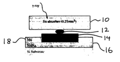
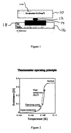
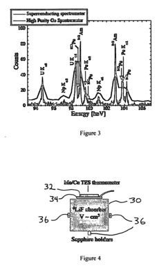
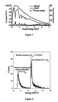
Superconducting gamma and fast-neutron spectrometers with high energy resolution
PatentInactiveUS20070075245A1
Innovation
- Development of superconducting gamma-ray and fast-neutron spectrometers operating at very low temperatures, utilizing a bulk absorber and a superconducting transition-edge sensor (TES) thermometer, which provides high energy resolution and efficient detection of gamma rays and neutrons, with the ability to differentiate between gamma and neutron scattering events.
Integrating a cryostat that hosts qubits with electronics for controlling the qubits
PatentWO2020154745A1
Innovation
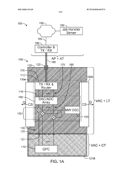
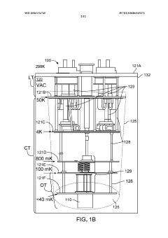
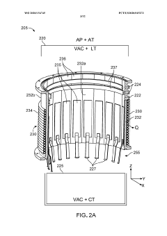
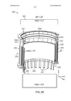
- Integrating control electronics, such as ADCs, DACs, FPGAs, and RF transceivers, directly into the cryostat's vacuum chamber to reduce the number of connections through the vacuum jacket, utilizing optical signals and RF flex cables for signal transmission, and employing a modular PCB design to efficiently manage control signals.
Materials Science Advancements for Cryogenic Applications
The evolution of cryogenic electronics, particularly quantum sensors, has been significantly propelled by breakthroughs in materials science. Traditional materials often fail under extreme low-temperature conditions, exhibiting brittleness, thermal contraction issues, and altered electrical properties. Recent advancements have focused on developing novel materials specifically engineered for cryogenic environments, enabling quantum sensing technologies to reach unprecedented levels of sensitivity and stability.
Superconducting materials represent one of the most critical developments in this field. High-temperature superconductors (HTS) like YBCO (Yttrium Barium Copper Oxide) have revolutionized quantum sensing by allowing operation at liquid nitrogen temperatures rather than requiring liquid helium. This advancement has made quantum sensing technologies more accessible and economically viable for broader applications.
Nanomaterials and thin-film technologies have emerged as game-changers for cryogenic electronics. Two-dimensional materials such as graphene and transition metal dichalcogenides (TMDs) maintain exceptional electrical properties at ultra-low temperatures while offering minimal thermal mass. These characteristics make them ideal for rapid thermal cycling and precise temperature control in quantum sensing applications.
Composite materials engineered specifically for cryogenic environments have addressed thermal expansion mismatch issues that previously plagued quantum sensor designs. Advanced ceramic-metal composites (cermets) and polymer-based composites with tailored coefficients of thermal expansion have enabled more robust and reliable sensor packaging solutions that maintain structural integrity across extreme temperature gradients.
Thermal management materials have seen remarkable innovation, with aerogels and advanced multi-layer insulation (MLI) systems providing superior thermal isolation. These materials create the stable thermal environments necessary for quantum sensors to operate at their theoretical performance limits, while minimizing cryogen consumption and extending operational lifetimes.
Interface materials that maintain reliable electrical connections between room temperature electronics and cryogenic sensing elements have been developed through novel metallization techniques and specialized solder alloys. These materials accommodate the significant thermal contraction that occurs during cooling while preserving electrical conductivity and mechanical integrity.
Radiation-hardened materials represent another frontier in cryogenic electronics, particularly for space-based quantum sensing applications. Advanced semiconductor materials doped with rare earth elements have demonstrated exceptional resilience to cosmic radiation while maintaining their electrical properties at cryogenic temperatures, extending the operational lifetime of quantum sensors in space environments.
The convergence of these materials science advancements has dramatically expanded the application scope of cryogenic quantum sensors, enabling new capabilities in fields ranging from medical imaging to fundamental physics research, while simultaneously reducing operational complexity and cost barriers.
Quantum Computing Integration Possibilities
The integration of cryogenic quantum sensor technologies with quantum computing systems represents a frontier with transformative potential for both fields. Quantum computers and quantum sensors share fundamental operational principles, particularly their reliance on quantum coherence and entanglement. This natural synergy creates opportunities for hybrid systems that leverage the strengths of both technologies.
Quantum sensors operating at cryogenic temperatures can serve as specialized input/output interfaces for quantum computers, enabling direct quantum-to-quantum data transfer without lossy classical conversion steps. This direct quantum information exchange could significantly reduce decoherence issues that currently limit quantum computing capabilities.
The development of integrated cryogenic platforms capable of simultaneously supporting quantum sensing and computing operations presents a particularly promising direction. Such platforms could enable real-time quantum feedback loops where sensor data directly influences quantum computational processes without leaving the quantum domain. This capability would be especially valuable for quantum simulation applications focused on materials science and chemical processes.
Several research groups have demonstrated preliminary integration of superconducting quantum interference device (SQUID) sensors with superconducting qubit architectures. These early demonstrations suggest that shared control electronics and readout systems can be developed to serve both sensing and computing functions, potentially reducing the overall system complexity and cost.
From an architectural perspective, quantum sensors could be incorporated as specialized quantum co-processors within larger quantum computing systems. These sensor co-processors could perform specific measurement tasks with quantum-enhanced precision while maintaining quantum coherence with the main computational qubits.
The integration challenges remain substantial, including maintaining compatible operating temperatures, managing electromagnetic interference between sensing and computing elements, and developing unified control systems. However, recent advances in cryogenic electronics, particularly in the development of cryogenic CMOS circuits and superconducting digital logic, are beginning to address these challenges.
Looking forward, quantum computing integration may drive new requirements for quantum sensor technologies, including the need for higher sensor densities, improved quantum state preparation fidelity, and more sophisticated quantum error correction capabilities. These requirements will likely accelerate innovation in both fields, creating a virtuous cycle of technological advancement.
Unlock deeper insights with PatSnap Eureka Quick Research — get a full tech report to explore trends and direct your research. Try now!
Generate Your Research Report Instantly with AI Agent
Supercharge your innovation with PatSnap Eureka AI Agent Platform!