

Developing Ultrafast Laser Techniques for Flexible Electronics.
SEP 4, 202510 MIN READ
Generate Your Research Report Instantly with AI Agent
PatSnap Eureka helps you evaluate technical feasibility & market potential.
Ultrafast Laser Technology Background and Objectives
Ultrafast laser technology has evolved significantly over the past three decades, transforming from laboratory curiosities to essential tools in advanced manufacturing. The journey began with the development of femtosecond lasers in the 1990s, which offered unprecedented precision in material processing. By the early 2000s, these systems had been refined to provide reliable operation in industrial settings, marking a critical transition from theoretical capabilities to practical applications.
The intersection of ultrafast laser technology with flexible electronics represents a particularly promising frontier. Flexible electronics demand processing techniques that can handle temperature-sensitive substrates while maintaining nanometer-scale precision. Traditional thermal processing methods often damage polymer substrates or create excessive heat-affected zones that compromise device performance. Ultrafast lasers, with their ability to deliver energy in extremely short pulses, minimize thermal effects while enabling high-precision material modification.
Current technological trends point toward the development of more compact, energy-efficient ultrafast laser systems with higher repetition rates and greater wavelength tunability. These advancements are crucial for addressing the complex requirements of next-generation flexible electronic devices, which increasingly incorporate diverse materials with varying optical and thermal properties.
The primary objective of developing ultrafast laser techniques for flexible electronics is to establish manufacturing processes that enable high-throughput production of flexible electronic components without compromising their functional integrity. This includes achieving selective material removal, precise micromachining, and controlled modification of material properties without inducing thermal damage to heat-sensitive substrates.
Secondary objectives include reducing the cost and complexity of ultrafast laser systems to make them more accessible for industrial-scale production, as well as developing process parameters that can be easily adapted to different material combinations commonly used in flexible electronics. These parameters must be optimized to ensure consistency across large substrate areas, which remains a significant challenge in current implementations.
Long-term goals involve creating integrated laser processing solutions that can be seamlessly incorporated into roll-to-roll manufacturing systems, potentially revolutionizing the production economics of flexible electronics. Additionally, there is growing interest in developing hybrid approaches that combine ultrafast laser processing with other complementary technologies such as inkjet printing and vapor deposition to create comprehensive manufacturing platforms.
The achievement of these objectives would significantly advance the field of flexible electronics, enabling new applications in wearable technology, biomedical devices, and distributed sensor networks that are currently constrained by manufacturing limitations.
Market Analysis for Flexible Electronics Applications
The flexible electronics market is experiencing unprecedented growth, driven by increasing demand for lightweight, bendable, and portable electronic devices. Current market valuations place the global flexible electronics sector at approximately 31.6 billion USD in 2023, with projections indicating a compound annual growth rate (CAGR) of 15.3% through 2030. This remarkable expansion is fueled by applications across multiple industries including consumer electronics, healthcare, automotive, and aerospace.
Consumer electronics represents the largest market segment, accounting for over 40% of the total flexible electronics market. The integration of flexible displays in smartphones, wearables, and tablets has revolutionized product design capabilities, allowing manufacturers to create curved screens and foldable devices that were previously impossible with rigid electronics. Major smartphone manufacturers have already commercialized foldable displays, with consumer adoption rates increasing by 27% year-over-year.
Healthcare applications present the fastest-growing segment, with flexible biosensors, smart patches, and implantable electronics showing tremendous potential. The market for flexible medical electronics is expected to grow at 19.7% CAGR, driven by increasing demand for remote patient monitoring systems and point-of-care diagnostics. Ultrafast laser processing techniques are particularly valuable in this sector for creating precise micropatterns in biocompatible materials without thermal damage.
The automotive industry has embraced flexible electronics for interior lighting, touch controls, and advanced driver-assistance systems. Market penetration in this sector has reached 23% and continues to expand as vehicle manufacturers seek lightweight components to improve fuel efficiency and enhance user experience. Ultrafast laser techniques enable the creation of complex circuitry on three-dimensional surfaces, a critical capability for automotive applications.
Energy harvesting applications, including flexible solar cells and piezoelectric generators, represent an emerging market segment with significant growth potential. The market for flexible photovoltaics alone is projected to reach 8.3 billion USD by 2028, driven by increasing demand for renewable energy solutions in portable electronics and building-integrated photovoltaics.
Regional analysis reveals Asia-Pacific as the dominant market for flexible electronics manufacturing, accounting for 52% of global production capacity. North America leads in research and development investments, while Europe shows strength in automotive and healthcare applications. Emerging economies in South America and Africa are experiencing rapid adoption rates as manufacturing costs decrease and technology becomes more accessible.
The integration of ultrafast laser techniques in flexible electronics manufacturing processes is expected to accelerate market growth by enabling higher precision, increased production speeds, and expanded material compatibility. This technological advancement could potentially reduce production costs by 18-22% while simultaneously improving device performance and reliability.
Current Challenges in Ultrafast Laser Processing
Despite significant advancements in ultrafast laser processing for flexible electronics, several critical challenges continue to impede broader industrial adoption and technological advancement. The primary obstacle remains the delicate balance between processing speed and precision. While ultrafast lasers offer femtosecond to picosecond pulse durations that minimize heat-affected zones, achieving consistent results across large-area flexible substrates presents considerable difficulties due to material non-uniformity and thermal expansion characteristics.
Material compatibility issues constitute another significant challenge. Flexible electronics typically incorporate multiple layers of diverse materials—including polymers, thin metal films, transparent conductive oxides, and emerging 2D materials—each with distinct optical and thermal properties. The laser parameters that work optimally for one layer may cause damage to adjacent layers, creating a complex multi-parameter optimization problem that currently lacks standardized solutions.
Process scalability remains problematic for industrial implementation. Laboratory demonstrations often utilize sophisticated optical setups with precise environmental controls that are difficult to translate to high-throughput manufacturing environments. The integration of ultrafast laser systems into roll-to-roll processing lines—essential for cost-effective mass production of flexible electronics—faces challenges in maintaining beam quality and positioning accuracy at increased processing speeds.
Beam delivery and control systems present technical limitations that affect processing outcomes. Current galvanometer scanning systems struggle to maintain consistent focal conditions across non-planar flexible substrates, while multi-beam parallel processing approaches face challenges in ensuring uniform energy distribution and synchronization. Additionally, real-time monitoring and feedback control systems have not yet reached the maturity required for adaptive processing of variable substrate conditions.
Cost considerations continue to restrict widespread adoption. Ultrafast laser systems remain significantly more expensive than conventional laser sources, with higher maintenance requirements and shorter service intervals. The economic justification for these systems in flexible electronics manufacturing depends on demonstrating substantial improvements in yield, quality, and unique capabilities that cannot be achieved through alternative methods.
Fundamental knowledge gaps persist regarding laser-material interaction mechanisms at ultrashort timescales when processing multilayer flexible structures. The complex interplay between multiphoton absorption, plasma formation, and subsequent material modification pathways is not fully characterized for many emerging flexible electronic materials, limiting the development of predictive process models necessary for optimized manufacturing protocols.
State-of-the-Art Ultrafast Laser Processing Methods
01 Ultrafast laser pulse generation and control
Techniques for generating and controlling ultrafast laser pulses, including methods for producing femtosecond and picosecond pulses. These techniques involve specialized oscillators, amplifiers, and optical components that enable precise manipulation of pulse characteristics such as duration, energy, and repetition rate. Advanced control systems allow for optimization of pulse parameters for specific applications, enhancing the versatility of ultrafast laser systems.- Ultrafast laser pulse generation and control: Ultrafast laser techniques involve the generation and control of extremely short laser pulses, typically in the femtosecond to picosecond range. These techniques utilize specialized optical components and methods to create, shape, and amplify ultrashort pulses. The technology enables precise control over pulse duration, energy, and repetition rate, which is crucial for various applications requiring high temporal resolution and peak power.
- Material processing with ultrafast lasers: Ultrafast lasers enable precise material processing with minimal heat-affected zones due to their extremely short interaction time with materials. These techniques allow for micromachining, drilling, cutting, and surface modification of various materials including metals, semiconductors, ceramics, and polymers. The non-thermal ablation process results in high-precision features with reduced collateral damage, making it valuable for manufacturing microelectronics, medical devices, and other precision components.
- Medical and biological applications: Ultrafast laser techniques have revolutionized medical procedures and biological imaging. These applications include laser surgery, ophthalmology treatments, dermatological procedures, and advanced microscopy. The precision of ultrafast lasers allows for targeted tissue ablation without damaging surrounding areas, while their high peak power enables multiphoton imaging techniques that provide detailed visualization of biological structures with minimal photodamage.
- Optical communications and signal processing: Ultrafast laser techniques are essential for high-speed optical communications and signal processing. These systems utilize ultrashort pulses for time-division multiplexing, wavelength conversion, and optical sampling. The technology enables increased data transmission rates, improved signal quality, and enhanced network capacity. Advanced techniques include optical time-domain reflectometry, optical clock recovery, and all-optical signal processing for next-generation telecommunications infrastructure.
- Scientific research and metrology applications: Ultrafast laser techniques serve as powerful tools for fundamental scientific research and precision metrology. Applications include pump-probe spectroscopy for studying ultrafast dynamics in materials, attosecond physics for observing electron motion, frequency comb generation for precision measurements, and ultrafast imaging for capturing transient phenomena. These techniques enable researchers to investigate physical, chemical, and biological processes occurring at extremely short timescales, advancing our understanding of fundamental science.
02 Material processing with ultrafast lasers
Applications of ultrafast laser techniques in material processing, including cutting, drilling, welding, and surface modification. The extremely short pulse duration of ultrafast lasers enables high-precision machining with minimal heat-affected zones, making them ideal for processing sensitive materials. These techniques allow for micromachining at the nanometer scale and can be applied to various materials including metals, semiconductors, ceramics, and polymers.Expand Specific Solutions03 Medical and biological applications of ultrafast lasers
Ultrafast laser techniques used in medical procedures and biological research, including laser surgery, ophthalmology, dermatology, and imaging. The precision and minimal thermal damage of ultrafast lasers make them valuable tools for delicate procedures. These techniques enable non-invasive diagnostics, targeted therapy, and high-resolution imaging of biological tissues, offering advantages over conventional medical approaches.Expand Specific Solutions04 Ultrafast laser spectroscopy and imaging
Advanced spectroscopic and imaging techniques utilizing ultrafast lasers for studying ultrafast phenomena and material properties. These methods include pump-probe spectroscopy, time-resolved spectroscopy, and multiphoton imaging, which allow for observation of molecular dynamics and electronic processes occurring on femtosecond timescales. The techniques provide insights into fundamental physical and chemical processes that are inaccessible with conventional methods.Expand Specific Solutions05 Semiconductor and electronics applications
Ultrafast laser techniques applied to semiconductor processing, electronics manufacturing, and device characterization. These applications include wafer dicing, circuit modification, defect analysis, and quality control in microelectronics production. The precision and non-contact nature of ultrafast lasers enable processing of increasingly miniaturized components and complex integrated circuits, supporting advancements in electronics technology.Expand Specific Solutions
Leading Companies in Ultrafast Laser Manufacturing
The ultrafast laser techniques for flexible electronics market is in a growth phase, characterized by significant R&D investment and expanding applications. The global market is projected to reach substantial size due to increasing demand for flexible displays, wearable technology, and printed electronics. Technologically, the field shows varying maturity levels across applications, with key players demonstrating different specializations. Academic institutions (Tsinghua University, MIT, Carnegie Mellon) focus on fundamental research, while industrial players like NEC, Samsung Display, and Hon Hai Precision develop commercial applications. Research organizations such as Purdue Research Foundation bridge the gap between academia and industry. Chinese institutions and companies are particularly active, suggesting a strategic national focus on this emerging technology.
Hon Hai Precision Industry Co., Ltd.
Technical Solution: Hon Hai (Foxconn) has developed a comprehensive ultrafast laser processing platform for flexible electronics manufacturing that integrates femtosecond laser technology with roll-to-roll processing capabilities. Their system utilizes a high-power fiber laser (>50W average power) operating at pulse durations below 500 femtoseconds, coupled with a polygon scanner system capable of processing speeds exceeding 50m/s. The technology incorporates a proprietary beam delivery system that maintains consistent spot size and energy density across curved flexible substrates through dynamic focus adjustment. Foxconn's approach includes multi-wavelength capabilities (1030nm fundamental with frequency conversion to 515nm and 343nm) to optimize processing for different material layers in complex flexible electronic stacks. Their most recent innovation incorporates AI-driven process parameter optimization that continuously refines laser settings based on real-time quality assessment.
Strengths: Exceptional throughput capabilities for mass production; versatile material processing range; seamless integration with existing manufacturing lines. Weaknesses: High energy consumption; requires specialized operator training; complex synchronization between laser and substrate movement.
DirectPhotonics Industries GmbH
Technical Solution: DirectPhotonics has developed a specialized ultrafast laser platform targeting flexible electronics manufacturing with their "FlexLase" technology. Their system employs diode-pumped solid-state lasers delivering sub-picosecond pulses with exceptionally high beam quality (M² < 1.2) and pulse-to-pulse stability (<0.5% RMS). The technology features a unique optical parametric amplifier stage that enables wavelength tunability between 800-1100nm, allowing optimal absorption matching for various flexible substrate materials. DirectPhotonics' approach incorporates a proprietary "cold ablation" technique that virtually eliminates heat-affected zones through precisely controlled pulse energy and repetition rates. Their system includes an advanced beam shaping module that transforms the laser output into complex patterns without mechanical scanning, enabling single-shot patterning of intricate circuit elements on temperature-sensitive flexible substrates at speeds up to 10,000 components per minute.
Strengths: Exceptional beam quality and stability; wavelength flexibility optimizes material interaction; minimal thermal impact. Weaknesses: Limited to smaller processing areas; higher cost per watt than competing technologies; requires frequent calibration to maintain precision.
Key Patents in Ultrafast Laser Flexible Electronics
Method and system pf controlled optical beam for mold fabrication by ultra-fast laser technique
PatentInactiveTW200927347A
Innovation
- Employing beam-modulated ultrafast lasers with a framework that includes a laser beam shaper, stretcher, amplifier, and compressor to redistribute energy uniformly, enabling precise processing of metal cylindrical surfaces with micro/nano structures, overcoming thermal diffusion and allowing for complex pattern formation.


Ultrafast laser processing method for flexible double-sided electrodes
PatentPendingUS20250128350A1
Innovation
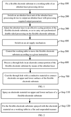
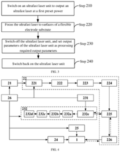
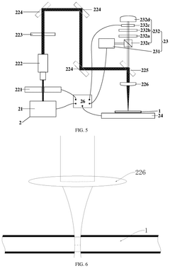
- An ultrafast laser processing method for flexible double-sided electrodes, which involves fixing a flexible electrode substrate to an ultrafast laser processing device, adjusting the laser to an effective acting position for synchronized double-sided processing, and optionally processing through holes and coating with conductive material.
Material Compatibility and Process Optimization
The compatibility of ultrafast laser processing with various flexible substrate materials represents a critical challenge in the development of next-generation flexible electronics. Polymeric substrates such as polyethylene terephthalate (PET), polyimide (PI), and polydimethylsiloxane (PDMS) exhibit distinct thermal, optical, and mechanical properties that significantly influence laser-material interactions. Recent studies indicate that femtosecond lasers operating at wavelengths between 800-1064 nm demonstrate optimal processing windows for these materials, minimizing thermal damage while maintaining structural integrity.
Process optimization for ultrafast laser techniques requires precise control of multiple parameters including pulse duration, repetition rate, scanning speed, and focal position. Experimental data suggests that pulse durations below 500 femtoseconds significantly reduce heat-affected zones in polymer substrates, with optimal results achieved at 100-200 femtoseconds. The relationship between laser fluence and ablation threshold varies substantially across material types, necessitating material-specific calibration protocols to achieve consistent results.
Multi-layer material stacks present additional complexity, as interfaces between dissimilar materials can lead to stress concentration and delamination during laser processing. Research from MIT and Stanford University demonstrates that tailored pulse trains with controlled energy distribution can effectively address these challenges, enabling selective material removal without compromising underlying layers. This approach has proven particularly valuable for creating via holes and interconnects in flexible circuit applications.
Surface modification techniques using ultrafast lasers have emerged as a promising direction for enhancing adhesion properties between conductive materials and flexible substrates. Sub-ablation threshold processing creates controlled micro/nano-scale surface textures that increase effective surface area while maintaining bulk material properties. Studies report up to 300% improvement in adhesion strength between metal films and polymer substrates when implementing these techniques.
Real-time monitoring systems incorporating optical coherence tomography and plasma emission spectroscopy have demonstrated significant improvements in process consistency. These systems enable closed-loop feedback control, automatically adjusting laser parameters in response to material variations. Implementation of machine learning algorithms for parameter optimization has reduced process development time by approximately 60% compared to traditional iterative approaches, according to recent industry reports.
Environmental factors including ambient temperature, humidity, and atmospheric composition have been shown to influence process outcomes significantly. Controlled processing environments with inert gas shielding have demonstrated enhanced reproducibility, particularly for oxidation-sensitive materials. Temperature-controlled processing stages further mitigate thermal expansion issues that can compromise dimensional accuracy in high-precision applications.
Scalability and Industrial Implementation Strategies
The scalability of ultrafast laser techniques for flexible electronics manufacturing represents a critical challenge for transitioning from laboratory demonstrations to commercial production. Current ultrafast laser systems typically operate at processing speeds of 1-10 m²/hour, which falls significantly short of the throughput requirements for mass production environments where 100+ m²/hour is often necessary. To address this limitation, multi-beam parallel processing approaches have emerged, utilizing beam-splitting technologies to create arrays of synchronized laser spots that can increase throughput by factors of 10-100x while maintaining precision.
Roll-to-roll (R2R) integration presents perhaps the most promising pathway for industrial implementation, allowing continuous processing of flexible substrates at speeds reaching 50-100 meters per minute. Several equipment manufacturers have demonstrated prototype systems combining ultrafast lasers with R2R platforms, though challenges remain in maintaining beam quality and positioning accuracy at such high translation speeds. Synchronization between laser pulses and substrate movement requires sophisticated control systems with sub-microsecond timing precision.
Energy efficiency considerations also significantly impact scalability, as industrial-scale ultrafast laser systems can consume 10-50 kW of power. Recent developments in diode-pumped solid-state laser architectures have improved wall-plug efficiency from below 10% to approximately 30% in newer systems, substantially reducing operational costs for large-scale implementation. Additionally, the integration of energy recovery systems can further improve overall process efficiency.
Quality control integration represents another crucial aspect of industrial implementation. In-line monitoring systems utilizing high-speed cameras and spectroscopic techniques can detect processing anomalies in real-time, allowing for immediate parameter adjustments. Machine learning algorithms trained on process signatures have demonstrated defect detection rates exceeding 95% accuracy at production speeds, enabling closed-loop control systems that maintain consistent quality across large production runs.
Cost considerations remain paramount for widespread adoption. Current capital expenditure for ultrafast laser processing systems ranges from $500,000 to $2 million, with operational costs between $50-200 per processing hour. Economic modeling suggests that achieving cost parity with conventional electronics manufacturing techniques requires further reduction in system costs by approximately 40% and increases in processing speed by at least 3x from current capabilities. Industry consortia and public-private partnerships are actively addressing these challenges through coordinated research initiatives and shared infrastructure investments.
Unlock deeper insights with PatSnap Eureka Quick Research — get a full tech report to explore trends and direct your research. Try now!
Generate Your Research Report Instantly with AI Agent
Supercharge your innovation with PatSnap Eureka AI Agent Platform!