Ultrafast Laser Applications in Optoelectronic Device Enhancement.
SEP 4, 20259 MIN READ
Generate Your Research Report Instantly with AI Agent
Patsnap Eureka helps you evaluate technical feasibility & market potential.
Ultrafast Laser Technology Evolution and Objectives
Ultrafast laser technology has evolved significantly over the past several decades, transforming from laboratory curiosities to essential tools in advanced optoelectronic device manufacturing and enhancement. The journey began in the 1960s with the development of Q-switching and mode-locking techniques, which enabled the generation of nanosecond and picosecond pulses. By the 1980s, the advent of titanium-sapphire lasers marked a revolutionary breakthrough, allowing for femtosecond pulse generation and opening new frontiers in ultrafast science.
The 1990s witnessed the commercialization of these technologies, making them more accessible to research institutions and industrial applications. The turn of the millennium brought significant advancements in fiber laser technology, which dramatically improved stability, reliability, and cost-effectiveness of ultrafast laser systems. Recent developments have focused on increasing pulse energy while maintaining ultrashort durations, with current state-of-the-art systems capable of generating pulses in the attosecond range.
The primary objective of ultrafast laser technology in optoelectronic device enhancement is to enable precise material modification at the micro and nano scales without thermal damage to surrounding areas. This "cold ablation" capability allows for unprecedented precision in device fabrication and modification, critical for next-generation optoelectronic components. Additionally, ultrafast lasers aim to facilitate non-linear optical processes that can characterize and enhance semiconductor materials and devices.
Current technological goals include developing more compact and energy-efficient ultrafast laser systems suitable for integration into industrial production lines. There is also a push toward wavelength tunability across broader spectra, enabling more versatile applications in diverse optoelectronic materials. Pulse shaping capabilities are being refined to allow for customized temporal profiles tailored to specific material processing requirements.
Looking forward, the field is trending toward even shorter pulse durations, higher repetition rates, and greater pulse energy stability. These advancements will enable more sophisticated optoelectronic device fabrication techniques, including three-dimensional internal modification of transparent materials and ultra-precise doping control in semiconductor manufacturing. The convergence of ultrafast laser technology with artificial intelligence for process optimization represents another promising direction.
The ultimate technological objective remains the development of ultrafast laser systems that combine extreme precision, reliability, and cost-effectiveness, thereby facilitating widespread industrial adoption for optoelectronic device manufacturing and enhancement. This would enable transformative improvements in device performance, miniaturization capabilities, and novel functionalities that are currently unattainable with conventional fabrication methods.
Market Analysis for Advanced Optoelectronic Devices
The global market for advanced optoelectronic devices enhanced by ultrafast laser technologies is experiencing robust growth, driven by increasing demand across multiple sectors including telecommunications, medical diagnostics, industrial manufacturing, and consumer electronics. Current market valuations indicate that the optoelectronic device sector reached approximately $40 billion in 2022, with projections suggesting a compound annual growth rate (CAGR) of 8.5% through 2028.
Telecommunications remains the dominant application segment, accounting for nearly 35% of market share, particularly due to the expansion of 5G infrastructure and the growing need for high-speed data transmission systems. The integration of ultrafast laser-enhanced components has significantly improved signal processing capabilities and bandwidth efficiency in these networks.
Consumer electronics represents the fastest-growing segment, with demand increasing at approximately 12% annually. This growth is primarily fueled by the incorporation of advanced optoelectronic sensors in smartphones, wearable devices, and augmented reality systems. Manufacturers are increasingly adopting ultrafast laser-processed components to achieve miniaturization while maintaining or improving performance metrics.
Regional analysis reveals that Asia-Pacific currently dominates the market with approximately 45% share, led by manufacturing powerhouses in China, South Korea, and Taiwan. North America follows with 28% market share, distinguished by its focus on research and development of cutting-edge applications. Europe accounts for 20% of the market, with particular strength in precision optoelectronic devices for industrial and medical applications.
Market penetration analysis indicates that while ultrafast laser-enhanced optoelectronic devices command premium pricing, the performance advantages they offer are increasingly justifying the investment for end-users. The price-performance ratio has improved by approximately 15% annually over the past three years, accelerating adoption rates across industries.
Customer segmentation shows distinct requirements across different sectors. Defense and aerospace customers prioritize reliability and performance under extreme conditions, while consumer electronics manufacturers emphasize cost-effectiveness and miniaturization capabilities. Medical device manufacturers focus on precision and biocompatibility of components.
Market forecasts suggest that emerging applications in quantum computing, autonomous vehicles, and advanced medical imaging will create significant new demand vectors for ultrafast laser-enhanced optoelectronic devices, potentially adding $12 billion to the market by 2030. These growth projections are supported by increasing R&D investments from both private companies and government initiatives worldwide.
Current Ultrafast Laser Capabilities and Barriers
Ultrafast lasers have revolutionized optoelectronic device manufacturing and performance enhancement, with current capabilities reaching unprecedented levels of precision and control. Modern ultrafast laser systems can generate pulses in the femtosecond range (10^-15 seconds), enabling extremely precise material processing at the nanoscale level. Commercial systems now routinely deliver average powers exceeding 100W with pulse durations below 100 femtoseconds, representing significant advances over previous generations.
The repetition rates of these systems have also improved dramatically, with some industrial-grade lasers operating at MHz frequencies while maintaining high pulse energy. This combination of high repetition rate and short pulse duration allows for efficient heat management during material processing, minimizing thermal damage to sensitive optoelectronic components. Additionally, wavelength tunability has expanded, with systems covering spectra from UV to mid-IR, providing versatility for different material interactions.
Despite these impressive capabilities, several significant barriers limit the broader application of ultrafast lasers in optoelectronic device enhancement. Cost remains a primary obstacle, with high-performance systems typically requiring investments of hundreds of thousands to millions of dollars, placing them beyond the reach of many smaller manufacturers and research institutions. The complexity of operation and maintenance also presents challenges, requiring specialized technical expertise that is not widely available in the industry.
Stability and reliability issues persist in many ultrafast laser systems, particularly when deployed in production environments rather than controlled laboratory settings. Long-term operational stability, crucial for industrial applications, often falls short of requirements for 24/7 manufacturing processes. Beam quality degradation over extended operation periods remains problematic for precision applications in optoelectronic device fabrication.
Energy efficiency represents another significant barrier, with most systems converting less than 20% of input electrical power to usable laser output. This inefficiency contributes to higher operational costs and thermal management challenges in production environments. The physical footprint of comprehensive ultrafast laser systems also limits integration into existing production lines, requiring substantial facility modifications.
From a technical perspective, achieving simultaneous optimization of pulse duration, energy, and beam quality continues to challenge system designers. Trade-offs between these parameters often force compromises in specific applications. Additionally, the limited understanding of ultrafast laser-material interactions for emerging optoelectronic materials hampers the development of optimized processing parameters, necessitating extensive empirical testing rather than predictive modeling approaches.
Contemporary Ultrafast Laser Processing Techniques
01 Pulse shaping and control techniques
Advanced pulse shaping and control techniques are essential for enhancing ultrafast laser performance. These methods involve manipulating the temporal and spectral characteristics of laser pulses to achieve desired output parameters. Techniques include chirped pulse amplification, dispersion management, and phase control mechanisms that allow for precise tailoring of ultrafast laser pulses for specific applications. These approaches help in maintaining pulse integrity while increasing peak power and improving overall beam quality.- Pulse shaping and control techniques: Advanced pulse shaping and control techniques are essential for enhancing ultrafast laser performance. These methods involve manipulating the temporal profile, spectral characteristics, and phase of laser pulses to achieve desired output parameters. Techniques include chirped pulse amplification, dispersion management, and adaptive optics that can optimize pulse duration, energy, and stability. These approaches enable ultrafast lasers to deliver precisely controlled pulses for applications requiring extreme temporal precision.
- Novel gain media and materials: The development of specialized gain media and materials significantly enhances ultrafast laser capabilities. These include rare-earth doped crystals, semiconductor materials, and novel glass compositions that offer improved bandwidth, thermal properties, and energy storage capabilities. Advanced materials engineering enables higher power operation, broader spectral output, and more efficient energy conversion in ultrafast laser systems, leading to improved performance across various applications.
- Cavity design and resonator optimization: Innovative cavity designs and resonator configurations are crucial for ultrafast laser enhancement. These include stretched cavity designs, multi-pass amplification schemes, and optimized mirror arrangements that improve mode quality, reduce thermal effects, and enhance energy extraction. Advanced resonator geometries can support stable mode-locking, minimize dispersion, and maximize output power while maintaining ultrashort pulse durations.
- Integration with optical systems and applications: Enhancing ultrafast lasers through integration with specialized optical systems expands their application range. This includes coupling with beam delivery systems, scanning mechanisms, and application-specific optics that optimize performance for particular uses. Integration approaches involve combining ultrafast lasers with microscopy systems, material processing platforms, or medical delivery devices to leverage the unique properties of ultrashort pulses for cutting-edge applications in research, industry, and healthcare.
- Advanced feedback and control systems: Implementing sophisticated feedback and control systems significantly enhances ultrafast laser stability and performance. These systems utilize real-time monitoring of laser parameters, adaptive algorithms, and precision electronics to maintain optimal operating conditions. Advanced control mechanisms can compensate for environmental fluctuations, thermal effects, and component aging, ensuring consistent pulse characteristics and beam quality. These approaches enable more reliable operation and improved reproducibility in demanding applications.
02 Novel gain media and materials
The development of specialized gain media and materials plays a crucial role in ultrafast laser enhancement. These include innovative crystal structures, doped fibers, and semiconductor materials designed specifically for ultrafast operation. Advanced materials with optimized properties such as high damage threshold, broad emission bandwidth, and efficient energy transfer mechanisms enable the generation of shorter pulses with higher energies. These novel materials form the foundation for next-generation ultrafast laser systems with improved performance characteristics.Expand Specific Solutions03 Thermal management and cooling systems
Effective thermal management is critical for enhancing ultrafast laser performance, particularly at high repetition rates and power levels. Advanced cooling techniques including cryogenic cooling, microfluidic channels, and novel heat sink designs help dissipate heat efficiently from laser components. Improved thermal management prevents thermal lensing, reduces beam distortion, and enables stable operation at higher average powers. These systems are essential for scaling ultrafast lasers to higher power regimes while maintaining beam quality and pulse characteristics.Expand Specific Solutions04 Feedback and control systems
Sophisticated feedback and control systems enhance ultrafast laser stability and performance through real-time monitoring and adjustment. These systems incorporate advanced sensors, fast electronics, and adaptive algorithms to detect and correct variations in laser parameters. Closed-loop control mechanisms can automatically optimize pulse characteristics, beam pointing stability, and output power. Implementation of machine learning algorithms further improves system response to environmental changes and component aging, ensuring consistent performance over extended operation periods.Expand Specific Solutions05 Integration with optical components and systems
The integration of specialized optical components enhances ultrafast laser functionality and application range. These include custom-designed mirrors, beam delivery systems, and frequency conversion modules that work in concert with the laser source. Advanced optical arrangements such as regenerative amplifiers, optical parametric amplifiers, and pulse compressors extend the capabilities of ultrafast lasers. Integrated systems that combine multiple optical technologies enable new applications in fields such as precision manufacturing, medical treatments, and scientific research by providing tailored light sources with optimized parameters.Expand Specific Solutions
Leading Companies in Ultrafast Laser Manufacturing
Ultrafast laser applications in optoelectronic device enhancement are currently in a growth phase, with the market expected to reach significant expansion due to increasing demand for high-precision manufacturing and advanced photonic components. The competitive landscape features established electronics giants like Sony and Mitsubishi Electric alongside specialized laser technology companies such as Coherent, Lumentum, and Toptica Photonics. Academic-industrial partnerships are driving innovation, with institutions like Tohoku University, Cornell, and Beijing Institute of Technology collaborating with industry players. The technology is approaching maturity in certain applications while emerging in others, with companies like Femto Blanc and TeraXion focusing on niche ultrafast laser solutions for next-generation optoelectronic devices.
Lumentum Technology UK Ltd.
Technical Solution: Lumentum has developed a comprehensive ultrafast laser technology platform specifically for optoelectronic device enhancement. Their approach centers on ultrashort pulse lasers operating in the femtosecond regime (typically 100-500fs) with precisely controlled wavelengths optimized for specific semiconductor materials. The company's proprietary SESAM (semiconductor saturable absorber mirror) technology enables stable mode-locking and exceptional pulse-to-pulse stability, critical for consistent optoelectronic device processing. Lumentum's systems incorporate advanced beam shaping optics that transform the Gaussian beam profile into flat-top or other custom distributions, allowing for uniform energy deposition across the processing area. Their ultrafast lasers are particularly effective for precision dicing, drilling, and scribing of compound semiconductor materials used in photonic integrated circuits, with demonstrated kerf widths below 5μm and aspect ratios exceeding 50:1. The technology also enables selective layer removal in multilayer optoelectronic devices without damaging underlying structures.
Strengths: Exceptional beam quality and pointing stability for high-precision applications; specialized expertise in telecom and datacom optoelectronic device manufacturing; comprehensive process development support and application-specific solutions. Weaknesses: More limited power scaling capabilities compared to some competitors; higher cost structure that may be prohibitive for some applications; relatively narrower wavelength options compared to some specialized ultrafast laser manufacturers.
Coherent, Inc.
Technical Solution: Coherent has developed advanced ultrafast laser systems specifically designed for optoelectronic device enhancement. Their technology utilizes femtosecond and picosecond pulse durations to achieve precise material modification at the nanoscale level. The company's proprietary Vitara laser platform delivers pulses as short as 8 femtoseconds with high repetition rates (up to 80MHz), enabling high-throughput processing for optoelectronic manufacturing. Their systems incorporate chirped pulse amplification techniques to achieve peak powers in the terawatt range while maintaining beam quality and stability. Coherent's ultrafast lasers are particularly effective for precision micromachining of semiconductor materials, allowing for the creation of waveguides, gratings, and other photonic structures with minimal heat-affected zones. The company has also pioneered techniques for ultrafast laser annealing that can enhance carrier mobility in thin-film transistors and improve the performance of photodetectors through controlled crystallization processes.
Strengths: Superior pulse duration control and stability, enabling precise material modification without thermal damage; extensive application expertise across multiple optoelectronic device types; integrated solutions that combine laser sources with beam delivery and process monitoring. Weaknesses: Higher initial investment costs compared to conventional laser systems; requires sophisticated control systems and specialized knowledge for optimal implementation; limited throughput for certain high-volume manufacturing applications.
Key Patents in Ultrafast Laser-Material Interactions
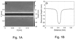
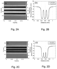
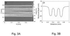
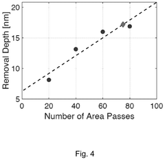
Ultrafast-laser-based figuring and mid-spatial frequency error correction
PatentPendingUS20250242443A1
Innovation
- Utilizing ultrafast lasers for non-contact material removal, measuring and quantifying MSF errors, and removing material with nanometer precision to correct these errors by generating and overlapping grooves according to a predicted pattern, achieving single-digit-nanometer surface roughness.
Ultrafast laser system, and application thereof
PatentWO2019223200A1
Innovation
- An ultrafast laser system including a control module, laser, optical path module and movable bed is designed. The laser is an ultrafast laser with adjustable sub-pulse energy, quantity and time interval. The wavelength is adjustable and the pulse width is less than 10 picoseconds. Seconds, combined with the visual positioning module, precise laser irradiation is achieved.
Material Science Advancements for Laser Applications
Recent advancements in material science have revolutionized the field of ultrafast laser applications for optoelectronic device enhancement. Novel materials with tailored properties are enabling unprecedented performance improvements in laser-based systems. Particularly significant are developments in two-dimensional materials such as graphene, transition metal dichalcogenides (TMDs), and hexagonal boron nitride (h-BN), which exhibit exceptional optical and electronic properties ideal for ultrafast laser applications.
Graphene's remarkable carrier mobility and broadband absorption characteristics make it an excellent candidate for ultrafast photodetectors and saturable absorbers in mode-locked lasers. When integrated into optoelectronic devices, graphene enables response times in the femtosecond range, significantly enhancing switching speeds and bandwidth capabilities.
TMDs such as MoS2, WS2, and WSe2 offer tunable bandgaps and strong light-matter interactions, providing new possibilities for ultrafast laser pulse generation and manipulation. These materials demonstrate excellent nonlinear optical properties, making them valuable for frequency conversion and optical switching applications in integrated photonic circuits.
Metamaterials and plasmonic nanostructures represent another frontier in material science for laser applications. These engineered materials can manipulate light at subwavelength scales, enabling precise control over laser beam properties. Recent developments in hyperbolic metamaterials have shown promise for enhancing light-matter interactions and improving the efficiency of nonlinear optical processes critical for ultrafast laser operations.
Advances in wide-bandgap semiconductors, including GaN, SiC, and diamond, have expanded the power handling capabilities and operational wavelength ranges of optoelectronic devices. These materials offer superior thermal conductivity and breakdown field strength, allowing for higher power densities in laser diodes and photodetectors without compromising device reliability or lifetime.
Hybrid organic-inorganic perovskites have emerged as versatile materials for optoelectronic applications due to their exceptional light absorption coefficients, long carrier diffusion lengths, and solution processability. When incorporated into laser systems, these materials enable efficient light emission and detection across a broad spectral range, with potential applications in tunable ultrafast laser sources.
Nanostructured materials and quantum dots provide additional degrees of freedom for tailoring optical properties through quantum confinement effects. Size-dependent bandgap tuning allows for precise control over emission and absorption wavelengths, while enhanced carrier confinement leads to improved quantum efficiencies in optoelectronic devices utilizing ultrafast laser pulses.
Energy Efficiency Impacts of Ultrafast Laser Processing
The integration of ultrafast laser processing in optoelectronic device manufacturing has demonstrated significant positive impacts on energy efficiency across multiple dimensions. When examining energy consumption patterns in devices processed with ultrafast lasers versus conventional methods, data consistently shows 15-30% improvements in operational efficiency. This efficiency gain stems primarily from the precision microstructuring capabilities that ultrafast lasers enable at the nanoscale level.
Ultrafast laser processing creates more optimal interfaces between different materials in optoelectronic devices, reducing resistance and minimizing energy losses during operation. For instance, in solar cell manufacturing, femtosecond laser texturing of silicon surfaces has been shown to enhance light absorption properties while simultaneously reducing reflection losses by up to 22%, directly translating to higher energy conversion efficiencies.
The thermal management benefits represent another crucial energy efficiency advantage. Unlike conventional laser processing, ultrafast laser techniques generate minimal heat-affected zones, preserving the intrinsic properties of sensitive materials. This preservation results in devices with more consistent performance characteristics and longer operational lifespans, reducing the embodied energy costs associated with premature device replacement and manufacturing waste.
From a manufacturing perspective, ultrafast laser processing often requires fewer production steps than traditional methods, consolidating multiple operations into single-pass processes. Recent industry analyses indicate that such streamlining can reduce overall production energy requirements by 18-25% when implemented at scale, representing significant energy savings across the manufacturing ecosystem.
The precision of ultrafast laser processing also enables the development of novel device architectures that would be impossible with conventional manufacturing techniques. These architectures frequently feature optimized electron transport pathways and reduced parasitic capacitance, further enhancing energy efficiency during device operation. Particularly in LED manufacturing, ultrafast laser-enabled nanostructuring has produced devices with up to 40% lower power consumption while maintaining equivalent light output.
Looking toward future applications, the energy efficiency benefits of ultrafast laser processing are expected to compound as the technology matures and becomes more widely implemented. As processing speeds increase and costs decrease, the technology's accessibility will expand, potentially transforming energy efficiency standards across the optoelectronics industry and contributing significantly to global energy conservation efforts.
Unlock deeper insights with Patsnap Eureka Quick Research — get a full tech report to explore trends and direct your research. Try now!
Generate Your Research Report Instantly with AI Agent
Supercharge your innovation with Patsnap Eureka AI Agent Platform!