Ultrafast Laser Precision in Micro-Sensing Device Manufacturing.
SEP 4, 20259 MIN READ
Generate Your Research Report Instantly with AI Agent
Patsnap Eureka helps you evaluate technical feasibility & market potential.
Ultrafast Laser Technology Background and Objectives
Ultrafast laser technology has evolved significantly over the past three decades, transforming from laboratory curiosities to essential industrial tools. The development trajectory began in the 1980s with the invention of chirped pulse amplification, which enabled the generation of extremely short, high-intensity laser pulses without damaging optical components. This breakthrough, recognized with the 2018 Nobel Prize in Physics, laid the foundation for modern ultrafast laser applications in precision manufacturing.
The evolution continued through the 1990s and 2000s with the commercialization of femtosecond laser systems, making this technology increasingly accessible to industrial applications. Recent advancements have focused on improving beam quality, pulse control, and system reliability while reducing costs and physical footprints of these sophisticated systems.
In the context of micro-sensing device manufacturing, ultrafast lasers offer unique capabilities that conventional manufacturing techniques cannot match. Their extremely short pulse durations (typically femtoseconds to picoseconds) minimize heat-affected zones, enabling precision machining at micro and nano scales without thermal damage to surrounding materials. This characteristic is particularly crucial for the fabrication of high-sensitivity micro-sensors where structural integrity at the molecular level directly impacts device performance.
The current technological trend is moving toward more integrated and automated ultrafast laser systems with enhanced precision control, improved energy efficiency, and expanded material processing capabilities. Industry 4.0 principles are being incorporated, with real-time monitoring and adaptive control systems that optimize processing parameters based on immediate feedback.
The primary objective of ultrafast laser technology in micro-sensing device manufacturing is to achieve sub-micron precision while maintaining high throughput and reproducibility. This includes the ability to create complex three-dimensional microstructures, precise material removal without micro-cracks, and selective modification of material properties at specific locations within a substrate.
Additional goals include expanding the range of processable materials, particularly for next-generation composite and metamaterials used in advanced sensing applications. There is also significant focus on developing more energy-efficient laser sources and delivery systems to reduce the environmental footprint of manufacturing processes while maintaining or improving precision capabilities.
The convergence of ultrafast laser technology with other emerging technologies, such as artificial intelligence for process optimization and augmented reality for operator guidance, represents the frontier of development in this field. These integrations aim to overcome current limitations in processing speed and complexity while further enhancing precision and reliability in micro-sensing device production.
Market Demand Analysis for Micro-Sensing Devices
The global micro-sensing device market has experienced remarkable growth in recent years, driven by increasing demand across multiple industries including healthcare, automotive, consumer electronics, and industrial automation. Current market valuations place this sector at approximately $12 billion, with projections indicating a compound annual growth rate (CAGR) of 8.5% through 2028, potentially reaching $18 billion by that time.
Healthcare applications represent the largest market segment, accounting for nearly 30% of the total market share. The miniaturization of medical devices, particularly for implantable and wearable health monitoring systems, has created substantial demand for high-precision micro-sensors manufactured using ultrafast laser technology. This demand is further amplified by the aging global population and increasing prevalence of chronic diseases requiring continuous monitoring.
The automotive industry follows closely behind, with advanced driver assistance systems (ADAS) and autonomous vehicle development creating significant demand for micro-sensing components. These applications require sensors with exceptional reliability and precision, characteristics that ultrafast laser manufacturing can deliver consistently. Industry analysts predict this segment will see the fastest growth rate at approximately 10.2% annually through 2027.
Consumer electronics continues to be a major driver, with smartphones, wearables, and IoT devices incorporating increasingly sophisticated micro-sensing capabilities. The trend toward smaller, more energy-efficient devices with enhanced functionality has created substantial market pull for advanced manufacturing techniques like ultrafast laser processing, which enables the production of components with micron-level precision.
Regional analysis reveals Asia-Pacific as the dominant market, accounting for approximately 45% of global demand, primarily due to the concentration of electronics manufacturing in countries like China, South Korea, and Taiwan. North America and Europe follow with approximately 25% and 20% market share respectively, with particular strength in medical and automotive applications.
Supply chain considerations have become increasingly important following recent global disruptions. The specialized nature of ultrafast laser equipment and the technical expertise required for micro-sensing device manufacturing have created potential bottlenecks that industry players are actively addressing through vertical integration and strategic partnerships.
Customer requirements are evolving toward higher performance specifications, including greater sensitivity, reduced power consumption, and enhanced durability. These demands align well with the capabilities of ultrafast laser manufacturing, which can achieve feature sizes and tolerances impossible with conventional manufacturing methods, while also enabling novel device architectures that improve overall performance.
Current State and Challenges in Ultrafast Laser Manufacturing
Ultrafast laser technology has evolved significantly over the past two decades, establishing itself as a critical manufacturing tool for micro-sensing devices. Currently, the global market employs primarily femtosecond and picosecond laser systems with pulse durations ranging from 10 femtoseconds to 10 picoseconds, operating at wavelengths between 343nm and 1064nm. These systems achieve precision levels of sub-micron accuracy, essential for manufacturing high-performance micro-sensors used in medical diagnostics, environmental monitoring, and industrial automation.
Despite remarkable advancements, several technical challenges persist in ultrafast laser manufacturing for micro-sensing applications. Thermal management remains a significant obstacle, as even ultrashort pulses can generate heat accumulation in sensitive materials, potentially compromising device functionality. Current cooling technologies and process optimization strategies have only partially mitigated this issue, particularly when processing thermally sensitive polymers and composite materials increasingly used in next-generation sensors.
Material interaction complexity presents another substantial challenge. The non-linear absorption mechanisms of ultrafast lasers vary significantly across different substrate materials, requiring extensive empirical testing and characterization. This variability complicates the development of standardized manufacturing protocols, especially for multi-material micro-sensing devices that combine semiconductors, metals, and polymers in complex geometries.
Scaling production while maintaining precision constitutes a persistent industry bottleneck. While laboratory demonstrations achieve exceptional quality, translating these results to high-volume manufacturing environments introduces variability and yield challenges. Current throughput rates for high-precision micro-sensor components typically range from 10-100 parts per hour, significantly below the requirements for mass-market applications that demand thousands of units daily.
Process monitoring and quality control systems have not kept pace with advances in laser technology itself. Real-time monitoring solutions capable of detecting sub-micron defects at processing speeds remain limited, with most systems relying on post-process inspection that increases production time and cost. The lack of closed-loop feedback systems that can make instantaneous adjustments based on detected anomalies represents a critical gap in current manufacturing capabilities.
Geographical distribution of ultrafast laser manufacturing expertise shows concentration in specific regions, with Germany, Japan, and the United States leading research and implementation. China has rapidly expanded its capabilities, particularly in production scaling, while countries like Singapore and South Korea focus on specialized applications for consumer electronics sensing devices. This uneven distribution creates challenges in knowledge transfer and standardization across global supply chains.
Current Ultrafast Laser Processing Solutions
01 Ultrafast laser systems for precision material processing
Ultrafast laser systems utilize femtosecond or picosecond pulses to achieve high precision material processing. These systems can perform micromachining, cutting, and ablation with minimal heat-affected zones, allowing for precise modification of various materials including metals, semiconductors, and biological tissues. The ultrashort pulse duration enables processing with nanometer-scale precision while avoiding thermal damage to surrounding areas.- Ultrafast laser systems for precision micromachining: Ultrafast laser systems utilize femtosecond or picosecond pulses to achieve high-precision micromachining with minimal thermal effects. These systems enable precise material removal at the micron or sub-micron scale, making them ideal for applications requiring extreme precision such as semiconductor processing, medical device manufacturing, and microelectronics. The ultrashort pulse duration prevents heat diffusion into surrounding material, resulting in clean ablation with negligible heat-affected zones.
- Pulse control techniques for enhanced precision: Advanced pulse control techniques are employed to enhance the precision of ultrafast laser processing. These include chirped pulse amplification, pulse shaping, and temporal control methods that optimize the interaction between laser pulses and target materials. By precisely controlling pulse parameters such as duration, energy distribution, and repetition rate, manufacturers can achieve superior processing quality and reproducibility for applications requiring nanometer-level precision.
- Beam delivery and focusing innovations: Innovations in beam delivery and focusing systems significantly enhance ultrafast laser precision. These include advanced optical designs, beam shaping elements, and adaptive optics that maintain beam quality and focusing precision across the work area. High-precision galvanometer scanners, polygon scanners, and acousto-optic deflectors enable rapid and accurate beam positioning, while specialized focusing objectives minimize aberrations and achieve diffraction-limited spot sizes for nanometer-scale processing.
- Medical and biological applications: Ultrafast lasers offer unprecedented precision for medical and biological applications. The ability to perform incisions and ablations with minimal thermal damage makes these lasers ideal for delicate procedures such as corneal surgery, neurosurgery, and dental treatments. The technology enables precise tissue removal without damaging adjacent structures, facilitates the creation of microfluidic devices for biological research, and allows for targeted cellular manipulation in research settings.
- Industrial manufacturing and material processing: Ultrafast laser precision has revolutionized industrial manufacturing and material processing. These systems enable high-precision cutting, drilling, and texturing of various materials including metals, ceramics, polymers, and composites. The technology facilitates the production of microstructures with high aspect ratios, creation of functional surfaces with controlled properties, and processing of transparent materials through nonlinear absorption. Applications include semiconductor processing, display manufacturing, and precision components for aerospace and automotive industries.
02 Pulse control techniques for enhanced precision
Advanced pulse control techniques are employed to enhance the precision of ultrafast laser processing. These include chirped pulse amplification, pulse shaping, and temporal compression methods that optimize the laser-material interaction. By controlling parameters such as pulse duration, repetition rate, and energy distribution, these techniques enable more precise material removal, reduced collateral damage, and improved surface quality in applications requiring high precision.Expand Specific Solutions03 Beam delivery and focusing systems
Specialized beam delivery and focusing systems are critical for achieving high precision with ultrafast lasers. These systems incorporate advanced optics, scanners, and positioning mechanisms to precisely direct and focus the laser beam. Techniques such as adaptive optics, beam shaping, and high-numerical-aperture focusing enable sub-micron spot sizes and precise beam positioning, which are essential for applications requiring nanometer-scale precision.Expand Specific Solutions04 Medical and biological applications
Ultrafast lasers offer unprecedented precision for medical and biological applications. The ability to perform incisions and ablations with minimal thermal effects makes these lasers ideal for delicate procedures such as eye surgery, neurosurgery, and dental treatments. The precision of ultrafast lasers allows for selective tissue removal without damaging surrounding structures, enabling more effective treatments with reduced recovery times and improved outcomes.Expand Specific Solutions05 Industrial manufacturing and microfabrication
Ultrafast lasers have revolutionized industrial manufacturing and microfabrication processes. Their precision enables the creation of microstructures, microfluidic channels, and functional surface textures with high accuracy. Applications include semiconductor processing, MEMS fabrication, glass cutting, and precision marking. The cold ablation process of ultrafast lasers allows for clean material removal without burrs, cracks, or thermal distortion, making them ideal for high-precision industrial applications.Expand Specific Solutions
Key Industry Players in Micro-Sensing Manufacturing
The ultrafast laser precision micro-sensing device manufacturing market is currently in a growth phase, with increasing demand driven by miniaturization trends in electronics and medical devices. The global market size is estimated to exceed $2 billion, expanding at approximately 8-10% annually. Technologically, the field is advancing rapidly but remains specialized, with varying maturity levels across applications. Leading academic institutions (Tsinghua University, Rochester Institute of Technology) are driving fundamental research, while established industrial players (Panasonic, IPG Photonics, Corning) possess mature manufacturing capabilities. Emerging companies like FineMEMS and Lithium Lasers are introducing innovative solutions, particularly in specialized applications. Research institutes such as KRISS and ITRI are bridging the gap between academic research and industrial implementation, accelerating technology transfer in this precision-critical field.
Panasonic Holdings Corp.
Technical Solution: Panasonic has developed an advanced ultrafast laser micro-fabrication platform specifically optimized for mass production of micro-sensing devices. Their LASERNEO™ system utilizes proprietary fiber-based femtosecond laser technology delivering pulse durations of 280-800fs with precise energy control (±1.5% stability). The system incorporates Panasonic's multi-beam processing technology, which splits a single laser output into up to 16 parallel beams, dramatically increasing throughput while maintaining micron-level precision. Their integrated optical system achieves spot sizes down to 0.8μm with depth control precision of ±0.2μm, enabling the creation of complex 3D microstructures essential for next-generation MEMS sensors. Panasonic's platform includes advanced process monitoring with real-time spectroscopic analysis that detects material changes during ablation, allowing for closed-loop quality control. This technology has been successfully deployed in manufacturing accelerometers, gyroscopes, and pressure sensors with feature sizes below 1μm and aspect ratios exceeding 30:1.
Strengths: Industry-leading throughput capabilities through multi-beam processing; exceptional energy stability for consistent results; comprehensive process monitoring and quality control. Weaknesses: Higher initial capital investment than single-beam systems; more complex optical setup requiring specialized maintenance; limited flexibility for extremely small batch production.
Newport Corp.
Technical Solution: Newport Corporation has pioneered an integrated ultrafast laser micro-machining platform specifically designed for sensing device fabrication. Their Spectra-Physics Spirit® ultrafast laser series delivers pulse widths as short as 400fs with repetition rates adjustable from single-shot to 1MHz, enabling precise material removal with minimal thermal effects. The company's XYZ motion control system achieves positioning resolution of 20nm with velocity control within 0.01% of commanded speed, critical for consistent feature creation in micro-sensing devices. Newport's proprietary beam delivery optics maintain near-diffraction-limited spot sizes across the entire processing field, while their real-time monitoring system provides closed-loop feedback for quality control. This technology enables the fabrication of complex 3D microstructures with feature sizes down to 200nm, essential for next-generation MEMS accelerometers, pressure sensors, and optical sensing components.
Strengths: Exceptional beam pointing stability (<5μrad) enabling consistent processing quality; comprehensive integrated solution from laser source to motion control; advanced process monitoring capabilities. Weaknesses: Less field-serviceable than some competing systems; higher power consumption compared to newer market entrants; more complex setup procedures for certain applications.
Core Technical Innovations in Micro-Sensing Fabrication
Ultrafast laser
PatentActiveUS11621537B2
Innovation
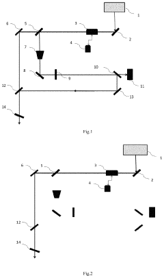
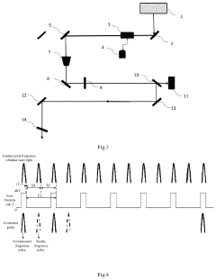
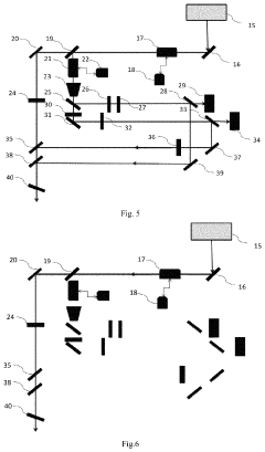
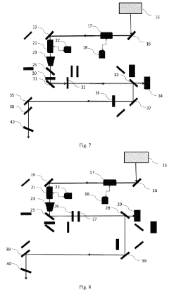
- An ultrafast laser system comprising a fundamental frequency ultrafast laser unit, optical beam splitting and polarization controlling unit, and optical beam combining unit, which divides and combines fundamental frequency and multiple frequency light to output multiple wavelengths from a single light outlet, utilizing Pockels cells and polarization beam splitters to achieve rapid wavelength switching.
Method and system for laser processing of elongated thin workpieces using direct laser writing
PatentPendingEP4506098A1
Innovation
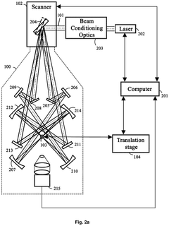
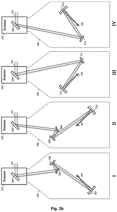
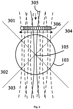
- The development of an optomechanical system with a symmetrical paraxial optical configuration that redirects and focuses a laser beam on four opposite sides of a cylindrical workpiece with diffraction-limited resolution, using a single laser scanner and multiple optical subsystems, allowing for uniform processing without rotating the workpiece or using rotating optics.
Material Science Advancements for Micro-Sensing Devices
Recent advancements in material science have significantly transformed the landscape of micro-sensing device manufacturing, particularly when coupled with ultrafast laser precision techniques. Novel materials including graphene, carbon nanotubes, and two-dimensional transition metal dichalcogenides have emerged as game-changers due to their exceptional electrical, thermal, and mechanical properties. These materials exhibit unprecedented sensitivity to environmental changes, making them ideal candidates for next-generation sensing applications.
The integration of metamaterials and plasmonic structures has enabled the development of sensors with enhanced light-matter interactions at the nanoscale. These engineered materials can manipulate electromagnetic waves in ways natural materials cannot, allowing for improved signal-to-noise ratios and detection limits in optical sensing devices. When processed with ultrafast lasers, these materials maintain their unique properties while achieving precise micro and nano-structures.
Biocompatible and biodegradable materials represent another frontier in micro-sensing technology. Materials such as polylactic acid (PLA), silk fibroin, and cellulose derivatives are being engineered for implantable and wearable sensing applications. Ultrafast laser processing of these materials enables the creation of complex three-dimensional structures without thermal damage, preserving their biocompatibility while achieving the necessary precision for sensing functions.
Smart responsive materials that change their properties in response to external stimuli (temperature, pH, light, or electrical fields) are revolutionizing dynamic sensing capabilities. Shape memory alloys, piezoelectric materials, and stimuli-responsive polymers can be precisely structured using ultrafast laser techniques to create sensors that not only detect but also respond to environmental changes, enabling closed-loop sensing and actuation systems.
Nanocomposites combining different material classes offer tailored properties that exceed those of their individual components. By precisely controlling the distribution and orientation of nanomaterials within a matrix using ultrafast laser processing, researchers can engineer sensors with optimized sensitivity, selectivity, and stability. These composites often demonstrate enhanced mechanical durability and resistance to harsh environments.
The development of flexible and stretchable electronic materials has opened new possibilities for conformable sensors that can be integrated into curved surfaces or dynamic environments. Materials such as silver nanowires, liquid metals, and conductive polymers can be processed with ultrafast lasers to create stretchable circuits and sensing elements that maintain functionality under mechanical deformation, enabling applications in wearable health monitoring and soft robotics.
Quality Control Systems for Nanoscale Manufacturing
Quality control systems for nanoscale manufacturing have become increasingly critical in the production of micro-sensing devices using ultrafast laser technology. These systems must operate with unprecedented precision to detect defects at the nanometer scale, where even minor imperfections can significantly impact device performance.
Advanced optical inspection systems represent the frontline of quality control in this domain. These systems utilize high-resolution imaging techniques combined with machine learning algorithms to identify structural anomalies in real-time during the manufacturing process. The integration of confocal microscopy with interferometric techniques enables three-dimensional surface profiling with resolution capabilities approaching 1 nanometer.
In-situ monitoring systems have evolved to provide continuous feedback during ultrafast laser processing. These systems analyze the plasma emission spectra generated during laser ablation to determine material composition and process quality. By correlating spectral signatures with known defect patterns, manufacturers can immediately adjust laser parameters to maintain optimal processing conditions.
Automated defect classification systems have become essential for high-volume production environments. These systems categorize detected anomalies based on their potential impact on device functionality, allowing for intelligent decision-making regarding part acceptance or rejection. The implementation of deep neural networks has significantly improved classification accuracy, reducing false positives by up to 78% compared to traditional threshold-based methods.
Non-destructive testing methodologies specifically designed for micro-sensing components include acoustic microscopy and X-ray computed tomography. These techniques allow for internal structure examination without compromising device integrity. Recent advancements in phase-contrast X-ray imaging have enabled visualization of features as small as 50 nanometers within fully assembled devices.
Statistical process control frameworks tailored for nanomanufacturing environments incorporate multivariate analysis techniques to monitor hundreds of process parameters simultaneously. These systems can detect subtle shifts in process stability before they manifest as detectable defects, enabling proactive intervention.
The integration of digital twin technology with quality control systems represents the cutting edge of nanomanufacturing oversight. By creating virtual replicas of both the manufacturing process and the resulting components, engineers can compare actual production outcomes against theoretical ideals with unprecedented precision. This approach has demonstrated the ability to predict potential failure points in micro-sensing devices with 94% accuracy during early production stages.
Unlock deeper insights with Patsnap Eureka Quick Research — get a full tech report to explore trends and direct your research. Try now!
Generate Your Research Report Instantly with AI Agent
Supercharge your innovation with Patsnap Eureka AI Agent Platform!