Ultrafast Laser Contributions to Nanostructured Thermoelectric Materials.
SEP 4, 202510 MIN READ
Generate Your Research Report Instantly with AI Agent
Patsnap Eureka helps you evaluate technical feasibility & market potential.
Ultrafast Laser Technology Evolution and Objectives
Ultrafast laser technology has evolved significantly over the past few decades, transforming from a laboratory curiosity to a powerful industrial tool with diverse applications. The journey began in the 1960s with the development of Q-switching and mode-locking techniques, which enabled the generation of nanosecond and picosecond pulses. By the 1980s, the advent of chirped pulse amplification (CPA) revolutionized the field, allowing for the generation of femtosecond pulses with unprecedented peak powers while avoiding damage to optical components.
The 1990s and early 2000s witnessed the commercialization of ultrafast laser systems, making them more accessible to researchers and industries. This period saw significant improvements in reliability, stability, and user-friendliness, transitioning these sophisticated tools from specialized physics laboratories to broader research and industrial settings. The development of fiber-based ultrafast lasers further enhanced their practicality and reduced maintenance requirements.
In recent years, ultrafast laser technology has experienced remarkable advancements in pulse duration, reaching the attosecond regime, while simultaneously achieving higher average powers and repetition rates. These improvements have expanded the application landscape, particularly in materials processing at the nanoscale, where precise energy deposition is crucial.
For thermoelectric materials, ultrafast lasers offer unique capabilities that conventional processing methods cannot match. The extremely short pulse duration allows for energy deposition faster than thermal diffusion, creating highly localized heating and rapid cooling rates exceeding 10^10 K/s. This non-equilibrium processing enables the formation of metastable phases and nanostructures that are otherwise unattainable through traditional methods.
The primary objective in applying ultrafast lasers to nanostructured thermoelectric materials is to enhance the figure of merit (ZT) by simultaneously increasing electrical conductivity while reducing thermal conductivity. This seemingly contradictory requirement can be addressed through precise nanostructuring, where ultrafast lasers excel due to their ability to create controlled defects, interfaces, and compositional gradients at the nanoscale.
Another key goal is to develop scalable manufacturing processes for high-performance thermoelectric materials. Current laboratory-scale demonstrations must evolve into economically viable production methods to enable widespread adoption of thermoelectric technologies for waste heat recovery and cooling applications. Ultrafast laser processing offers promising pathways toward this industrialization through high processing speeds and compatibility with roll-to-roll manufacturing.
Additionally, researchers aim to achieve greater control over the morphology and composition of nanostructures within thermoelectric materials, enabling precise engineering of electron and phonon transport properties. The ultimate objective is to design thermoelectric materials with tailored electronic and thermal properties that approach theoretical efficiency limits, potentially revolutionizing energy recovery systems and thermal management technologies.
Market Analysis for Nanostructured Thermoelectric Applications
The global market for nanostructured thermoelectric materials has been experiencing significant growth, driven by increasing demand for energy-efficient solutions across multiple industries. Current market valuations indicate that the thermoelectric materials market reached approximately 51 million USD in 2020 and is projected to grow at a compound annual growth rate of 8.3% through 2027, with nanostructured materials representing the fastest-growing segment.
The automotive sector represents the largest application market for nanostructured thermoelectric materials, particularly in waste heat recovery systems. Major automotive manufacturers including BMW, Ford, and Toyota have initiated research programs to integrate thermoelectric generators into vehicle exhaust systems, potentially improving fuel efficiency by 3-5% by converting waste heat into usable electricity.
Consumer electronics constitutes another rapidly expanding market segment, with thermoelectric cooling solutions being integrated into high-performance computing systems, smartphones, and wearable devices. The miniaturization capabilities offered by ultrafast laser processing of nanostructured thermoelectric materials align perfectly with the industry's demand for smaller, more efficient cooling solutions.
The medical and aerospace sectors are emerging as promising markets for advanced thermoelectric applications. In medical devices, precise temperature control enabled by nanostructured thermoelectric materials is critical for diagnostic equipment, drug storage, and implantable devices. The aerospace industry values the reliability and lack of moving parts in thermoelectric systems for satellite thermal management and aircraft sensor cooling.
Regional market analysis reveals that North America and Asia-Pacific currently dominate the nanostructured thermoelectric materials market. North America leads in research and development activities, while Asia-Pacific, particularly China, Japan, and South Korea, excels in manufacturing capacity and implementation. Europe is rapidly gaining market share through aggressive green technology initiatives and automotive industry adoption.
Market barriers include the relatively high production costs of nanostructured thermoelectric materials and the technical complexity of integrating ultrafast laser processing into existing manufacturing workflows. However, these barriers are gradually diminishing as production scales increase and processing technologies mature.
Customer demand patterns indicate growing interest in materials with higher ZT values (thermoelectric figure of merit), with particular emphasis on environmentally friendly compositions that reduce or eliminate toxic elements like tellurium and lead. This trend aligns well with ultrafast laser processing capabilities, which can enhance the performance of more sustainable material alternatives through precise nanostructuring.
The market outlook for ultrafast laser-processed nanostructured thermoelectric materials remains highly positive, with projected market penetration accelerating as energy efficiency regulations tighten globally and renewable energy integration creates new opportunities for thermal energy harvesting technologies.
Current Challenges in Laser-Based Thermoelectric Material Fabrication
Despite significant advancements in ultrafast laser processing for thermoelectric materials, several critical challenges persist that limit widespread industrial adoption and optimal performance. Precise control of nanostructure formation remains a fundamental obstacle, as the complex interaction between ultrafast laser pulses and target materials often produces inconsistent feature sizes and distributions. This variability directly impacts the thermoelectric properties, particularly the crucial figure of merit ZT, which requires simultaneous optimization of electrical conductivity, thermal conductivity, and Seebeck coefficient.
Scalability presents another significant hurdle, as most current ultrafast laser processing techniques demonstrate excellent results at laboratory scale but face difficulties in transitioning to industrial production volumes. The inherently serial nature of laser processing creates throughput limitations that affect commercial viability, while maintaining consistent quality across larger surface areas requires sophisticated beam delivery and positioning systems that add complexity and cost.
Material-specific optimization poses additional challenges, as different thermoelectric compounds respond uniquely to laser parameters. The optimal processing window—including pulse duration, energy density, repetition rate, and scanning strategy—varies significantly between bismuth telluride, lead telluride, silicon-germanium alloys, and emerging organic thermoelectric materials. This necessitates extensive empirical testing for each material system, slowing development cycles.
Process integration difficulties arise when attempting to incorporate laser-processed thermoelectric materials into functional devices. Thermal management during processing remains problematic, as excessive heat accumulation can degrade thermoelectric properties or create unwanted phase transformations. Additionally, laser-induced defects and oxidation can negatively impact long-term stability and performance of the processed materials.
Characterization and quality control represent persistent challenges, as real-time monitoring of nanostructure formation during ultrafast laser processing remains limited. Current analytical techniques often require post-processing examination, making in-situ adjustments difficult and increasing production costs through additional quality control steps.
Energy efficiency concerns also exist, as high-power ultrafast laser systems consume significant energy, potentially offsetting some of the efficiency gains offered by the improved thermoelectric materials they produce. This creates a sustainability paradox that must be addressed through system optimization and more efficient laser sources.
Finally, the fundamental physics governing ultrafast laser-material interactions for thermoelectric applications remains incompletely understood. The complex interplay between photon absorption, electron-phonon coupling, thermal transport, and phase transformations during ultrashort pulse interactions creates modeling challenges that limit predictive capabilities and necessitate continued basic research alongside applied development efforts.
State-of-the-Art Ultrafast Laser Processing Techniques
01 Nanostructured thermoelectric materials with enhanced ZT values
Nanostructured thermoelectric materials exhibit significantly improved thermoelectric figure of merit (ZT) compared to their bulk counterparts. The nanostructuring creates quantum confinement effects and increases phonon scattering at interfaces, which reduces thermal conductivity while maintaining electrical conductivity. These materials often incorporate quantum dots, nanowires, or superlattice structures to optimize the power factor and achieve higher energy conversion efficiency.- Nanostructured thermoelectric materials with enhanced ZT values: Nanostructured thermoelectric materials exhibit significantly improved thermoelectric figure of merit (ZT) compared to their bulk counterparts. The nanostructuring creates quantum confinement effects and increases phonon scattering at interfaces, which reduces thermal conductivity while maintaining electrical conductivity. These materials often incorporate quantum dots, nanowires, or superlattice structures to optimize the power factor and achieve higher energy conversion efficiency.
- Semiconductor-based thermoelectric nanomaterials: Semiconductor-based thermoelectric nanomaterials, particularly those containing bismuth telluride, lead telluride, silicon-germanium alloys, and skutterudites, demonstrate superior thermoelectric properties. These materials are engineered at the nanoscale to create band structure modifications and energy filtering effects that enhance the Seebeck coefficient. The controlled doping and composition tuning of these semiconductor nanomaterials allow for optimized carrier concentration and mobility, resulting in improved thermoelectric performance across different temperature ranges.
- Fabrication methods for nanostructured thermoelectric materials: Various fabrication techniques are employed to create nanostructured thermoelectric materials with controlled dimensions and properties. These methods include ball milling followed by spark plasma sintering, solution-based synthesis, vapor deposition, and molecular beam epitaxy. Each technique offers different advantages in terms of scalability, cost-effectiveness, and the ability to create specific nanostructures such as quantum dots, nanowires, or thin films. The processing parameters significantly influence the final thermoelectric properties by affecting grain size, crystallinity, and interface characteristics.
- Interface engineering in thermoelectric nanocomposites: Interface engineering plays a crucial role in enhancing thermoelectric properties of nanocomposites. By creating numerous interfaces between different materials or phases, phonon transport is disrupted while electron transport is maintained, leading to reduced thermal conductivity without significantly affecting electrical conductivity. Techniques such as grain boundary engineering, inclusion of nanoprecipitates, and creation of core-shell structures are employed to optimize interface density and characteristics. The controlled introduction of defects at interfaces further enhances phonon scattering and improves thermoelectric performance.
- Novel nanostructured thermoelectric materials for specific applications: Novel nanostructured thermoelectric materials are being developed for specific applications such as wearable devices, automotive waste heat recovery, and space exploration. These materials include organic-inorganic hybrids, flexible thermoelectric films, and materials optimized for extreme temperature conditions. Research focuses on enhancing stability, flexibility, and compatibility with various substrates while maintaining high thermoelectric performance. Environmental considerations are also driving the development of lead-free and earth-abundant thermoelectric nanomaterials that can provide sustainable energy harvesting solutions.
02 Semiconductor-based thermoelectric nanomaterials
Semiconductor-based thermoelectric nanomaterials, particularly those containing bismuth telluride, lead telluride, silicon-germanium alloys, and skutterudites, demonstrate superior thermoelectric properties. These materials are engineered at the nanoscale to create band structure modifications and energy filtering effects that enhance the Seebeck coefficient. The controlled doping and composition tuning of these semiconductor nanomaterials allow for optimized carrier concentration and mobility, resulting in improved thermoelectric performance across different temperature ranges.Expand Specific Solutions03 Fabrication methods for nanostructured thermoelectric materials
Advanced fabrication techniques for nanostructured thermoelectric materials include ball milling, spark plasma sintering, molecular beam epitaxy, and solution-based synthesis methods. These processes enable precise control over grain size, interface density, and compositional homogeneity, which are critical factors affecting thermoelectric performance. Post-processing treatments such as annealing and hot pressing are employed to optimize the microstructure and reduce defects, thereby enhancing carrier mobility and thermoelectric properties.Expand Specific Solutions04 Composite and hybrid nanostructured thermoelectric materials
Composite and hybrid nanostructured thermoelectric materials combine different material systems to leverage complementary properties and overcome limitations of single-phase materials. These composites often incorporate carbon nanotubes, graphene, or metal nanoparticles into conventional thermoelectric matrices to create additional interfaces for phonon scattering while maintaining electrical pathways. The synergistic effects between the constituent materials lead to enhanced power factors and reduced thermal conductivity, resulting in superior thermoelectric performance across broader temperature ranges.Expand Specific Solutions05 Novel nanostructured thermoelectric materials for specific applications
Novel nanostructured thermoelectric materials are being developed for specific applications such as wearable electronics, automotive waste heat recovery, and space exploration. These materials are designed to operate efficiently under particular conditions, including flexible substrates, high-temperature environments, or extreme temperature gradients. Recent innovations include organic-inorganic hybrid thermoelectrics, environmentally friendly alternatives to toxic elements, and materials with self-healing properties to enhance long-term stability and performance in real-world applications.Expand Specific Solutions
Leading Research Institutions and Industrial Manufacturers
The ultrafast laser technology for nanostructured thermoelectric materials is in an emerging growth phase, with the global market expanding rapidly due to increasing demand for efficient energy harvesting solutions. Current market size is estimated to be moderate but growing, driven by applications in waste heat recovery and renewable energy sectors. Technologically, the field shows varying maturity levels across players. Research institutions like Tsinghua University, Beijing University of Technology, and University of California lead academic innovation, while companies such as Alphabet Energy and 3M are advancing commercial applications. Fraunhofer-Gesellschaft and National Research Council of Canada bridge the research-industry gap. Asian universities, particularly Chinese institutions, demonstrate significant research momentum, while established corporations like Sony and Toshiba focus on integrating these technologies into broader energy solutions.
Beijing University of Technology
Technical Solution: Beijing University of Technology has developed an innovative ultrafast laser-based approach for enhancing thermoelectric materials through controlled nanostructuring. Their technique employs femtosecond laser pulses to create precise nanoporous structures in thermoelectric materials, significantly reducing thermal conductivity while maintaining electrical properties. The process utilizes a unique spatial light modulator system that enables customized nanopattern generation across various thermoelectric materials including Bi2Te3, PbTe, and skutterudite compounds. Their research has demonstrated that laser-induced nanostructures can reduce thermal conductivity by up to 45% while preserving electrical conductivity, resulting in ZT value improvements of approximately 30-40%. The university has also pioneered a hybrid approach combining ultrafast laser processing with subsequent chemical treatment to further optimize the nanostructure morphology and stability at elevated operating temperatures, addressing a key challenge in thermoelectric device implementation.
Strengths: Highly customizable nanostructure patterns; excellent control over feature size and distribution; process compatibility with multiple thermoelectric material systems; innovative hybrid processing approaches. Weaknesses: Relatively slower processing speed compared to some bulk manufacturing methods; potential challenges in scaling to industrial production volumes; higher energy consumption compared to some chemical nanostructuring methods.
Fraunhofer-Gesellschaft eV
Technical Solution: Fraunhofer-Gesellschaft has developed a comprehensive ultrafast laser processing platform for thermoelectric nanostructuring. Their approach utilizes femtosecond laser pulses to create precisely controlled nanostructures in thermoelectric materials, enhancing phonon scattering while preserving electron transport pathways. The technology employs a multi-beam interference technique that creates periodic nanostructures with feature sizes below 100 nm, significantly reducing thermal conductivity. Their process allows for selective modification of material surfaces without affecting bulk properties, creating quantum confinement effects that enhance the Seebeck coefficient. Fraunhofer has demonstrated ZT value improvements of up to 40% in bismuth telluride compounds through their laser-based nanostructuring approach, and has successfully scaled the technology for industrial applications using high-repetition-rate laser systems.
Strengths: Precise control over nanostructure dimensions and patterns; scalable for industrial production; non-contact processing method that minimizes contamination; compatible with various thermoelectric materials. Weaknesses: Higher initial equipment costs compared to chemical methods; potential for thermal damage in heat-sensitive materials; limited penetration depth requiring multiple processing passes for bulk materials.
Key Patents and Scientific Breakthroughs in Thermoelectric Nanomaterials
Laser direct synthesis and deposit of nanocomposite materials or nanostructures
PatentInactiveEP3094760A1
Innovation
- A method involving a laser beam opaque inorganic target with an organic layer on its backside is used to create hybrid nanocomposite materials through direct synthesis and deposition onto a substrate, allowing for one-step and one-technological-cycle production of hybrid nanocomposites with precise control over location and properties, avoiding damage to organic materials and eliminating the need for additional stages or expensive equipment.
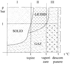
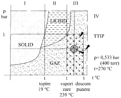
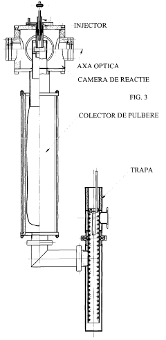
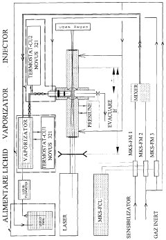
High efficiency laser installation for the synthesis of nanostructures from liquid precursors of high toxicity and hazard by thermal vaporization to obtain gas phase at temperatures higher than the boiling temperature limit and lower than the decomposition temperature limit, with automatic precision and accuracy control of temperature up to 500°c and highly reproductible synthesis
PatentUndeterminedRO126660A0
Innovation
- A high-production laser synthesis system that utilizes a two-stage thermal vaporization process to maintain precursors in the gas phase above the vaporization temperature, ensuring precise multi-point temperature control and preventing condensation or decomposition, with a vaporizer designed for temperatures up to 500 °C and a system for continuous operation.
Environmental Impact and Sustainability Considerations
The integration of ultrafast laser technology in the production of nanostructured thermoelectric materials presents significant environmental implications that warrant careful consideration. The manufacturing processes involved in traditional thermoelectric material production often require energy-intensive methods and potentially hazardous chemicals. Ultrafast laser processing offers a more environmentally friendly alternative by reducing the need for toxic chemical etching agents and minimizing waste generation through precise material manipulation at the nanoscale.
Energy consumption during manufacturing represents a critical environmental factor. Ultrafast laser systems, while requiring substantial power during operation, demonstrate superior energy efficiency when considering the entire production lifecycle. The precision of laser processing reduces material waste by up to 30% compared to conventional methods, contributing to resource conservation and decreased environmental footprint. Additionally, the ability to process materials at room temperature in many applications eliminates the need for energy-intensive heating processes.
Raw material utilization efficiency is markedly improved through ultrafast laser techniques. The technology enables the creation of complex nanostructures with minimal material loss, addressing concerns about the scarcity of rare earth elements and other critical materials commonly used in thermoelectric devices. This efficiency extends the availability of limited resources and reduces the environmental impact associated with mining and processing these materials.
The operational benefits of laser-processed thermoelectric materials also contribute to environmental sustainability. Enhanced conversion efficiency in thermoelectric generators means more waste heat can be recaptured and converted to useful electricity, potentially reducing fossil fuel consumption in various industrial applications. Studies indicate that nanostructured thermoelectric materials produced using ultrafast laser techniques can improve conversion efficiency by 15-25% compared to conventional materials.
End-of-life considerations reveal additional environmental advantages. The precise control over material composition and structure facilitated by ultrafast laser processing can simplify recycling processes. The reduced use of toxic compounds in manufacturing also means less hazardous waste management concerns when devices reach end-of-life. Furthermore, the durability of laser-processed materials potentially extends product lifecycles, reducing replacement frequency and associated resource consumption.
Carbon footprint analyses of the entire production and utilization cycle demonstrate that despite the initial energy investment in laser processing equipment, the environmental benefits accumulate significantly over time. The combination of manufacturing efficiency, improved device performance, and extended product lifespan contributes to an estimated 40% reduction in lifetime carbon emissions compared to conventionally manufactured thermoelectric systems.
Scalability and Commercial Viability Assessment
The scalability of ultrafast laser processing for nanostructured thermoelectric materials presents both significant opportunities and challenges for commercial implementation. Current laboratory-scale demonstrations have shown promising results in enhancing thermoelectric efficiency through precise nanostructuring, but transitioning to industrial-scale production requires substantial technological advancement and investment.
Production throughput remains a primary concern, as ultrafast laser processing typically operates on small surface areas at a time. Recent innovations in beam splitting and parallel processing techniques have improved throughput by factors of 5-10x compared to traditional single-beam approaches, yet still fall short of requirements for mass production. Multi-beam processing systems and high-repetition-rate lasers (>MHz) are emerging as potential solutions, with preliminary studies indicating possible processing speeds compatible with roll-to-roll manufacturing.
Cost considerations present another significant barrier to commercialization. The capital expenditure for industrial-grade ultrafast laser systems ranges from $500,000 to $2 million, with additional costs for precision positioning systems and environmental controls. Operating expenses, including maintenance, energy consumption, and skilled personnel, further impact the economic viability. Current cost estimates suggest that laser-processed thermoelectric materials would need to achieve 30-40% higher efficiency than conventional materials to justify the additional manufacturing expense.
Energy consumption analysis reveals that ultrafast laser processing requires 2-5 kWh per square meter of processed material, depending on the specific nanostructuring requirements. This energy investment must be recovered through improved thermoelectric performance within a reasonable timeframe to ensure commercial viability.
Market readiness assessment indicates that certain high-value applications could justify current production costs. Specialized sectors such as aerospace, medical devices, and high-performance computing represent potential early adoption markets where performance advantages outweigh cost considerations. Consumer applications remain several years from economic viability without significant process optimization.
Scaling pathways have been identified through industry-academic partnerships. Integration with existing manufacturing lines, rather than standalone processing, appears most promising for near-term implementation. Hybrid approaches combining ultrafast laser processing for critical features with conventional techniques for bulk production could provide a transitional pathway to full-scale commercialization.
Regulatory considerations and material supply chain stability must also be addressed before widespread adoption. The specialized nature of high-performance thermoelectric materials often involves elements with limited availability or geopolitical supply constraints, potentially affecting long-term commercial viability.
Unlock deeper insights with Patsnap Eureka Quick Research — get a full tech report to explore trends and direct your research. Try now!
Generate Your Research Report Instantly with AI Agent
Supercharge your innovation with Patsnap Eureka AI Agent Platform!