Ultrafast Laser Techniques for Transparent Conductive Film Creation.
SEP 4, 20259 MIN READ
Generate Your Research Report Instantly with AI Agent
Patsnap Eureka helps you evaluate technical feasibility & market potential.
Ultrafast Laser TCF Technology Background and Objectives
Transparent conductive films (TCFs) represent a critical component in modern optoelectronic devices, serving as essential elements in touchscreens, displays, solar cells, and smart windows. Historically, indium tin oxide (ITO) has dominated this field since the 1950s due to its excellent combination of optical transparency and electrical conductivity. However, ITO's inherent limitations—including brittleness, scarcity of indium resources, and high processing temperatures—have driven extensive research into alternative TCF technologies over the past two decades.
Ultrafast laser processing has emerged as a revolutionary approach for TCF creation, offering unprecedented precision in material modification at the nanoscale. This technology utilizes femtosecond or picosecond lasers that deliver extremely short pulses (10^-15 to 10^-12 seconds), enabling material interaction without significant heat diffusion—a phenomenon known as "cold ablation." The evolution of this technology began in the early 2000s with fundamental research and has accelerated dramatically since 2010 with the commercialization of more stable and accessible ultrafast laser systems.
The primary objective of ultrafast laser TCF technology development is to create conductive patterns on transparent substrates with minimal optical impact while maintaining electrical performance comparable to or exceeding that of ITO. Specifically, the technology aims to achieve sheet resistance below 100 Ω/sq with optical transparency above 90% in the visible spectrum, while enabling flexibility that traditional ITO cannot provide.
Current research focuses on several key technical goals: optimizing laser parameters for various substrate materials, developing scalable manufacturing processes for industrial implementation, enhancing the long-term stability of laser-processed TCFs, and reducing production costs to compete with established technologies. Additionally, researchers are exploring multi-material approaches where ultrafast lasers can selectively modify composite structures to create gradient properties within a single film.
The technology trajectory suggests potential breakthroughs in direct-write processes that eliminate photolithography steps, in-situ monitoring systems for real-time quality control, and integration with roll-to-roll manufacturing for high-throughput production. These advancements would position ultrafast laser TCF technology as a viable solution for next-generation flexible electronics, wearable devices, and building-integrated photovoltaics.
As environmental considerations gain prominence, another critical objective is developing eco-friendly TCF production methods. Ultrafast laser processing offers advantages in this regard through reduced chemical waste compared to conventional wet etching processes, lower energy consumption than vacuum deposition techniques, and compatibility with sustainable substrate materials.
Market Analysis for Transparent Conductive Films
The transparent conductive film (TCF) market has experienced significant growth in recent years, driven primarily by the expanding electronics industry and increasing demand for touch-enabled devices. The global TCF market was valued at approximately 5.1 billion USD in 2022 and is projected to reach 8.3 billion USD by 2028, growing at a CAGR of 8.4% during the forecast period.
Consumer electronics remains the dominant application segment, accounting for over 60% of the market share. This is largely attributed to the widespread adoption of smartphones, tablets, and other touch-enabled devices that require high-performance TCFs. The automotive sector represents the fastest-growing segment, with increasing integration of touch panels in vehicle infotainment systems and the rising production of electric vehicles incorporating advanced display technologies.
Regionally, Asia-Pacific dominates the TCF market, holding approximately 65% of the global market share. This dominance is primarily due to the presence of major electronics manufacturers in countries like China, Japan, South Korea, and Taiwan. North America and Europe follow, with market shares of approximately 18% and 12% respectively, driven by technological advancements and high consumer spending on electronic devices.
The market for ultrafast laser-processed TCFs specifically is emerging as a high-growth subsegment. While currently representing less than 5% of the total TCF market, it is expected to grow at a CAGR of 15.2% through 2028, significantly outpacing the overall market growth. This accelerated growth is driven by the superior performance characteristics of laser-processed films, including higher transparency, better conductivity, and improved flexibility compared to conventionally manufactured alternatives.
Key market drivers include the growing demand for flexible and foldable displays, increasing adoption of OLED technology, and the push for more sustainable manufacturing processes. The ultrafast laser technique addresses several pain points in traditional TCF manufacturing, including material waste reduction and enhanced performance parameters, making it particularly attractive for high-end applications.
Market challenges include high initial equipment costs for ultrafast laser systems and competition from alternative technologies such as silver nanowires and metal mesh. However, as production scales and technology matures, cost barriers are expected to diminish, further accelerating market penetration of laser-processed TCFs.
Current Challenges in Ultrafast Laser Processing
Despite significant advancements in ultrafast laser processing for transparent conductive film (TCF) creation, several critical challenges continue to impede broader industrial adoption and optimal performance. The fundamental challenge lies in achieving the delicate balance between optical transparency and electrical conductivity, as these properties typically exhibit inverse relationships in most processing scenarios.
Material interaction complexity presents a significant hurdle, as ultrafast lasers interact with transparent substrates through nonlinear absorption mechanisms that are highly dependent on pulse characteristics. The multiphoton absorption and plasma formation processes remain difficult to precisely control across different material compositions, leading to inconsistent results when scaling from laboratory to production environments.
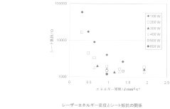
Process parameter optimization remains exceptionally complex due to the multidimensional nature of variables involved. Pulse duration, repetition rate, wavelength, polarization, scanning speed, and focal position must be simultaneously optimized for each specific material system. The interdependence of these parameters creates an expansive solution space that is challenging to navigate efficiently, even with advanced machine learning approaches.
Heat accumulation effects pose particular difficulties when processing at high repetition rates necessary for industrial throughput. While ultrafast lasers are known for "cold ablation," the cumulative thermal effects at megahertz repetition rates can compromise the intended non-thermal nature of processing, leading to undesired material modifications and reduced conductivity-transparency performance.
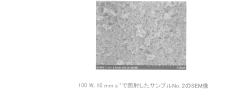
Scalability and throughput limitations represent significant industrial barriers. Current processing speeds remain insufficient for large-area applications like touch panels and solar cells. While polygon scanner systems have improved processing speeds, they introduce beam quality variations across the scanning field that affect feature consistency and electrical performance.
Quality control and process monitoring capabilities lag behind processing technology. Real-time assessment of electrical and optical properties during fabrication remains challenging, with most quality verification occurring post-processing. This delayed feedback loop extends development cycles and increases production costs.
Long-term stability of laser-processed TCFs presents ongoing concerns, particularly regarding oxidation resistance and mechanical durability under bending or stretching conditions. Environmental factors can gradually degrade the conductive pathways created through laser processing, limiting application in flexible electronics and outdoor installations.
Standardization across different laser systems and processing environments is notably absent, making it difficult to transfer optimized parameters between different manufacturing setups. This lack of standardized protocols hinders broader industrial adoption and slows technology transfer from research to production environments.
Material interaction complexity presents a significant hurdle, as ultrafast lasers interact with transparent substrates through nonlinear absorption mechanisms that are highly dependent on pulse characteristics. The multiphoton absorption and plasma formation processes remain difficult to precisely control across different material compositions, leading to inconsistent results when scaling from laboratory to production environments.
Process parameter optimization remains exceptionally complex due to the multidimensional nature of variables involved. Pulse duration, repetition rate, wavelength, polarization, scanning speed, and focal position must be simultaneously optimized for each specific material system. The interdependence of these parameters creates an expansive solution space that is challenging to navigate efficiently, even with advanced machine learning approaches.
Heat accumulation effects pose particular difficulties when processing at high repetition rates necessary for industrial throughput. While ultrafast lasers are known for "cold ablation," the cumulative thermal effects at megahertz repetition rates can compromise the intended non-thermal nature of processing, leading to undesired material modifications and reduced conductivity-transparency performance.
Scalability and throughput limitations represent significant industrial barriers. Current processing speeds remain insufficient for large-area applications like touch panels and solar cells. While polygon scanner systems have improved processing speeds, they introduce beam quality variations across the scanning field that affect feature consistency and electrical performance.
Quality control and process monitoring capabilities lag behind processing technology. Real-time assessment of electrical and optical properties during fabrication remains challenging, with most quality verification occurring post-processing. This delayed feedback loop extends development cycles and increases production costs.
Long-term stability of laser-processed TCFs presents ongoing concerns, particularly regarding oxidation resistance and mechanical durability under bending or stretching conditions. Environmental factors can gradually degrade the conductive pathways created through laser processing, limiting application in flexible electronics and outdoor installations.
Standardization across different laser systems and processing environments is notably absent, making it difficult to transfer optimized parameters between different manufacturing setups. This lack of standardized protocols hinders broader industrial adoption and slows technology transfer from research to production environments.
State-of-the-Art Ultrafast Laser TCF Solutions
01 Ultrafast laser patterning of transparent conductive films
Ultrafast laser techniques are used for precise patterning of transparent conductive films (TCFs). The femtosecond or picosecond laser pulses allow for high-precision ablation with minimal thermal damage to the surrounding material. This technique enables the creation of intricate patterns and circuits on TCFs while maintaining their optical transparency and electrical conductivity properties, which is crucial for applications in touch screens, displays, and photovoltaic devices.- Ultrafast laser patterning of transparent conductive films: Ultrafast laser techniques are used for precise patterning of transparent conductive films. The femtosecond or picosecond laser pulses allow for high-precision ablation and structuring of the conductive layers without damaging the underlying substrate. This technique enables the creation of intricate electrode patterns for touch screens, displays, and other electronic devices while maintaining optical transparency and electrical conductivity.
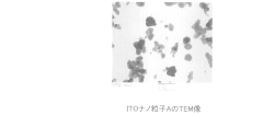
- Laser-induced modification of transparent conductive oxides: Ultrafast lasers can be used to modify the properties of transparent conductive oxides (TCOs) such as indium tin oxide (ITO) and zinc oxide (ZnO). The high-intensity, short-duration pulses can alter the crystalline structure, oxygen content, or doping concentration in these materials, allowing for controlled changes in conductivity and transparency. This technique enables the creation of gradient-index materials or selective modification of electrical properties without compromising optical transparency.
- Laser-assisted deposition of transparent conductive films: Ultrafast laser techniques can be employed in the deposition process of transparent conductive films. Pulsed laser deposition (PLD) using femtosecond or picosecond lasers allows for the precise control of film thickness, composition, and structure. The high-energy, short-duration pulses can ablate target materials and create plasma plumes that deposit uniform thin films with excellent optical and electrical properties, suitable for various optoelectronic applications.
- Laser sintering of nanoparticle-based transparent conductive films: Ultrafast laser sintering is used to process nanoparticle-based transparent conductive films. The technique involves applying short, intense laser pulses to sinter metallic nanoparticles (such as silver or copper) into continuous conductive networks while maintaining transparency. This approach allows for low-temperature processing of flexible substrates and enables the fabrication of bendable or stretchable transparent electrodes for flexible electronics and displays.
- Laser-induced reduction for transparent conductive film fabrication: Ultrafast laser techniques can be used for the selective reduction of metal oxide precursors to create transparent conductive patterns. The high-intensity laser pulses trigger photochemical or photothermal reduction processes that convert non-conductive metal oxide compounds into conductive metallic structures. This direct-write approach enables maskless patterning of transparent conductive elements and can be performed at ambient conditions, reducing manufacturing complexity and cost.
02 Laser-induced modification of TCF material properties
Ultrafast laser techniques can be used to modify the material properties of transparent conductive films without complete ablation. By controlling laser parameters such as pulse duration, energy density, and scanning speed, it's possible to selectively alter the electrical conductivity, optical transparency, and mechanical properties of TCFs. This approach allows for gradient property changes and localized modifications that are difficult to achieve with conventional processing methods.Expand Specific Solutions03 Fabrication of TCFs using ultrafast laser deposition
Ultrafast laser deposition techniques, including pulsed laser deposition (PLD), can be used to fabricate high-quality transparent conductive films. The ultrashort laser pulses create a plasma plume from target materials, which then deposits onto substrates to form thin films with controlled thickness and composition. This method allows for the deposition of various materials including indium tin oxide (ITO), zinc oxide, and carbon-based materials to create TCFs with tailored properties.Expand Specific Solutions04 Laser annealing and crystallization of TCFs
Ultrafast laser techniques can be employed for post-deposition treatment of transparent conductive films through annealing and crystallization processes. The high-intensity, short-duration laser pulses provide localized heating that improves film crystallinity and reduces defects without damaging temperature-sensitive substrates. This process enhances electrical conductivity while maintaining optical transparency, and can be performed selectively on specific areas of the film.Expand Specific Solutions05 Nanostructuring of TCFs using ultrafast lasers
Ultrafast laser techniques enable the creation of nanostructures on transparent conductive films that can enhance their performance. By generating controlled surface textures, nanopatterns, or periodic structures at the nanoscale, the optical and electrical properties of TCFs can be significantly improved. These nanostructures can reduce reflection, enhance light trapping, improve conductivity, and create unique functional properties for advanced applications in optoelectronics and photonics.Expand Specific Solutions
Leading Companies in Ultrafast Laser TCF Industry
The ultrafast laser techniques for transparent conductive film creation market is in a growth phase, characterized by increasing adoption across electronics, automotive, and energy sectors. The market is expanding rapidly with an estimated size of several billion dollars, driven by demand for flexible displays, touchscreens, and photovoltaics. Technologically, the field shows varying maturity levels with established players like IMRA America, Sumitomo Electric, and Panasonic leading commercial applications, while research institutions such as Fraunhofer-Gesellschaft, RIKEN, and Qingdao University of Technology push fundamental innovations. Companies like JOLED and Konica Minolta are advancing specialized applications in display technologies, while Furukawa Electric and Hon Hai Precision focus on scaling manufacturing processes. The ecosystem demonstrates a healthy balance between industrial commercialization and academic research advancement.
IMRA America, Inc.
Technical Solution: IMRA America has pioneered ultrafast fiber laser technology for transparent conductive film (TCF) creation. Their approach utilizes femtosecond laser pulses with precisely controlled parameters to directly pattern metal nanoparticles onto transparent substrates. The company's FCPA (Fiber Chirped Pulse Amplification) technology delivers high-energy ultrashort pulses that enable selective ablation and modification of thin films without thermal damage to underlying substrates. Their proprietary process involves laser-induced forward transfer (LIFT) techniques that can deposit conductive materials with sub-micron precision. IMRA's systems operate at high repetition rates (>100 kHz) allowing for industrial-scale throughput while maintaining nanoscale feature resolution. The company has developed specialized beam delivery systems that optimize the laser-material interaction for TCF applications, resulting in films with transparency >90% and sheet resistance <100 ohms/square.
Strengths: Superior precision in patterning capability with minimal thermal effects; scalable process suitable for industrial production; ability to create complex patterns without masks. Weaknesses: Higher initial equipment costs compared to conventional methods; requires sophisticated control systems; process optimization needed for different substrate materials.
Sumitomo Electric Industries Ltd.
Technical Solution: Sumitomo Electric Industries has developed a sophisticated ultrafast laser technique for transparent conductive film creation that builds upon their extensive expertise in materials science and precision manufacturing. Their approach utilizes ultrashort pulse lasers operating in the sub-picosecond regime to selectively modify the surface properties of specialized polymer substrates infused with conductive nanoparticles. The process involves a proprietary multi-pass laser treatment that creates interconnected networks of conductive pathways while preserving optical transparency. Sumitomo's technology incorporates adaptive optics systems that compensate for material variations in real-time, ensuring consistent processing quality across large substrate areas. Their method achieves remarkable uniformity in electrical properties, with sheet resistance variation less than ±5% across 1-meter-wide substrates. The company has also developed a unique laser-assisted doping technique that enhances conductivity in specific regions without compromising transparency, enabling the creation of gradient conductivity profiles tailored for specific applications. Sumitomo's TCFs demonstrate exceptional environmental stability, maintaining performance specifications after extended exposure to high humidity (85% RH) and elevated temperatures (85°C) for over 1000 hours.
Strengths: Outstanding uniformity across large areas; excellent environmental stability and durability; capability to create customized conductivity profiles within a single film. Weaknesses: Higher processing complexity requiring sophisticated control systems; more energy-intensive than some competing methods; specialized substrate requirements that may limit material options.
Key Patents in Ultrafast Laser TCF Processing
Method for producing transparent conductive film
PatentInactiveJP2012094284A
Innovation
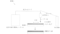
- A method involving the use of laser irradiation with wavelengths between 700 to 2200 nm, particularly using continuous-wave GaAs-AlGaInP-based or InP-GaInAsP-based semiconductor lasers, to penetrate and reduce sheet resistance in thick transparent conductive films, combined with the use of ITO nanoparticles and InSn complexes to further enhance conductivity.
Laser patterning of dual sided transparent conductive films
PatentWO2015164024A1
Innovation
- A method involving a transparent conductive film with a substrate and two conductive layers of metal nanostructures on opposing sides, where a laser is used to pattern one layer without affecting the other, utilizing radiation absorbing or reflective compounds to reduce transmission and maintain high visible light transmission.
Environmental Impact of Laser TCF Manufacturing
The manufacturing of transparent conductive films (TCFs) using ultrafast laser techniques presents both environmental challenges and opportunities compared to conventional methods. Traditional TCF production often relies on chemical-intensive processes and rare materials like indium, which pose significant environmental concerns. Ultrafast laser techniques offer a more environmentally conscious alternative by reducing chemical waste and enabling more efficient material utilization.
Energy consumption represents a critical environmental factor in laser-based TCF manufacturing. While ultrafast laser systems require substantial power during operation, their precision and efficiency can result in lower overall energy consumption per unit of production compared to conventional methods. Recent advancements in laser technology have improved energy efficiency by up to 40%, with fiber laser systems demonstrating particularly promising results in reducing the carbon footprint of TCF production.
Waste reduction constitutes another significant environmental advantage of laser-based TCF manufacturing. The precise nature of ultrafast laser processing minimizes material waste through targeted ablation and modification processes. Studies indicate that laser-based techniques can reduce material waste by 30-50% compared to traditional wet chemical etching methods, substantially decreasing the environmental burden associated with waste disposal and treatment.
The reduced reliance on toxic chemicals represents perhaps the most substantial environmental benefit of laser TCF manufacturing. Conventional TCF production typically involves hazardous substances such as acids, heavy metals, and volatile organic compounds. Ultrafast laser techniques largely eliminate the need for these chemicals, resulting in cleaner production processes with minimal toxic emissions and effluent discharge. This transition significantly reduces water pollution risks and workplace hazards.
Life cycle assessments of laser-based TCF manufacturing have demonstrated a 25-35% reduction in overall environmental impact compared to conventional methods. These assessments consider factors including raw material extraction, energy consumption, waste generation, and end-of-life disposal. The extended operational lifespan of laser-produced TCFs further enhances their environmental credentials by reducing replacement frequency and associated resource consumption.
Despite these advantages, challenges remain in optimizing the environmental performance of laser TCF manufacturing. Current research focuses on developing more energy-efficient laser sources, implementing closed-loop material recovery systems, and exploring alternative substrate materials with lower environmental footprints. Addressing these challenges will be crucial for maximizing the environmental benefits of this promising technology as it continues to evolve and gain wider industrial adoption.
Cost-Benefit Analysis of Ultrafast Laser TCF Production
The implementation of ultrafast laser techniques for transparent conductive film (TCF) creation requires careful economic evaluation to determine its viability in commercial settings. Initial capital expenditure for ultrafast laser systems represents a significant investment, with industrial-grade femtosecond laser setups ranging from $200,000 to $500,000, depending on power specifications, pulse characteristics, and automation capabilities. Additional costs include specialized optical components, precision positioning systems, and environmental control infrastructure, potentially adding 30-50% to the base system cost.
Operational expenses must be considered alongside capital costs. Energy consumption for high-power ultrafast laser systems can reach 10-30 kW during operation, translating to substantial utility costs in production environments. Maintenance requirements include regular replacement of optical components (typically every 3-6 months), laser gain medium servicing, and cooling system maintenance, collectively accounting for approximately 8-12% of the initial system cost annually.
However, these costs must be balanced against the significant benefits of ultrafast laser TCF production. Production efficiency metrics indicate that laser-based techniques can achieve processing speeds of 0.5-2 m²/min, depending on pattern complexity and required conductivity specifications. This represents a 30-40% improvement over conventional chemical etching methods. Material utilization efficiency is particularly noteworthy, with laser techniques reducing material waste by up to 60% compared to traditional subtractive methods.
Quality improvements provide additional economic value. Laser-produced TCFs demonstrate 15-25% higher optical transparency at equivalent conductivity levels compared to conventional ITO films. Mechanical flexibility tests show 3-5 times greater bend resistance before conductivity degradation, extending product lifespans in flexible electronics applications. These performance advantages translate to premium pricing potential in high-value markets such as OLED displays, touch panels, and photovoltaics.
Return on investment calculations suggest that despite higher initial capital costs, ultrafast laser TCF production systems can achieve breakeven within 18-30 months in high-volume manufacturing scenarios. This timeline is heavily dependent on production volume, with facilities processing over 10,000 m² annually achieving faster returns. Sensitivity analysis indicates that material cost savings and premium pricing for higher-quality outputs are the most significant factors affecting ROI, more so than energy efficiency or labor cost reductions.
Unlock deeper insights with Patsnap Eureka Quick Research — get a full tech report to explore trends and direct your research. Try now!
Generate Your Research Report Instantly with AI Agent
Supercharge your innovation with Patsnap Eureka AI Agent Platform!