Investigating Ultrafast Laser Fabrication of Embedded Circuits.
SEP 4, 202510 MIN READ
Generate Your Research Report Instantly with AI Agent
Patsnap Eureka helps you evaluate technical feasibility & market potential.
Ultrafast Laser Fabrication Background and Objectives
Ultrafast laser fabrication of embedded circuits represents a revolutionary approach in the field of electronics manufacturing, marking a significant departure from traditional circuit fabrication methods. This technology has evolved over the past two decades from experimental laboratory demonstrations to increasingly sophisticated industrial applications. The fundamental principle involves using ultrashort laser pulses—typically in the femtosecond to picosecond range—to modify materials with unprecedented precision, enabling the creation of three-dimensional conductive pathways within various substrates.
The historical trajectory of ultrafast laser technology began in the 1990s with the development of reliable femtosecond laser systems. By the early 2000s, researchers demonstrated the ability to create localized modifications in transparent materials, laying the groundwork for embedded circuit fabrication. The field gained significant momentum between 2010-2015 when several research groups successfully demonstrated functional embedded electronic components in glass and polymer substrates.
Current technological trends indicate a shift toward higher processing speeds, greater precision, and expanded material compatibility. The integration of advanced beam shaping techniques and multi-beam processing approaches has dramatically increased fabrication efficiency, while developments in laser sources have extended the wavelength ranges available for processing different materials.
The primary objectives of ultrafast laser fabrication research center on addressing several critical challenges. First, achieving higher circuit density and complexity within embedded structures remains a fundamental goal. Second, improving the electrical performance of laser-fabricated circuits to match or exceed that of conventional electronics represents a significant technical hurdle. Third, developing scalable manufacturing processes that maintain precision while increasing throughput is essential for commercial viability.
Additional objectives include expanding the range of compatible substrate materials beyond glass and certain polymers to include flexible substrates and ceramics. There is also considerable interest in developing hybrid approaches that combine ultrafast laser processing with complementary technologies such as inkjet printing or vapor deposition to create more sophisticated embedded systems.
From a strategic perspective, ultrafast laser fabrication aims to enable entirely new device architectures that are impossible with traditional fabrication methods. These include truly three-dimensional electronic circuits, embedded sensors in structural components, and electronics integrated directly into optical systems. The ultimate goal is to establish a versatile manufacturing platform that can produce highly customized, geometrically complex electronic systems with minimal material waste and environmental impact.
Market Demand for Embedded Circuit Technologies
The embedded circuit technology market is experiencing robust growth driven by increasing demand for miniaturization and integration in electronic devices. The global market for embedded circuits was valued at approximately 9.8 billion USD in 2022 and is projected to reach 15.3 billion USD by 2027, representing a compound annual growth rate of 9.2%. This growth trajectory is primarily fueled by advancements in ultrafast laser fabrication techniques that enable the creation of more compact, efficient, and reliable embedded circuits.
The automotive industry represents one of the largest market segments for embedded circuit technologies, accounting for nearly 28% of the total market share. The transition toward electric vehicles and autonomous driving systems has significantly increased the demand for sophisticated embedded circuits that can withstand harsh operating conditions while maintaining high performance standards. Automotive manufacturers are particularly interested in ultrafast laser-fabricated embedded circuits due to their enhanced thermal management capabilities and reduced form factors.
Consumer electronics constitutes another substantial market segment, with smartphones, wearables, and IoT devices driving demand for miniaturized embedded circuits. The consumer electronics sector values the ability of ultrafast laser fabrication to create intricate circuit patterns within limited spaces, enabling the development of increasingly compact and feature-rich devices. Market research indicates that approximately 65% of consumer electronics manufacturers are exploring or implementing embedded circuit technologies in their product roadmaps.
The medical device industry represents a rapidly growing market for embedded circuit technologies, with applications ranging from implantable devices to diagnostic equipment. The biocompatibility and reliability of ultrafast laser-fabricated embedded circuits make them particularly suitable for medical applications where device failure is not an option. Industry analysts project that the medical embedded circuits segment will grow at a rate of 12.5% annually through 2028, outpacing the overall market growth.
Industrial automation and aerospace sectors are also showing increased interest in embedded circuit technologies. These industries require robust electronic components that can function reliably in extreme environments, making them ideal candidates for ultrafast laser-fabricated embedded circuits. The industrial automation sector alone is expected to contribute approximately 2.1 billion USD to the embedded circuits market by 2025.
Regional analysis reveals that Asia-Pacific dominates the embedded circuits market with a 42% share, followed by North America (27%) and Europe (21%). China, Japan, South Korea, and Taiwan are the primary manufacturing hubs, while research and development activities are concentrated in the United States, Germany, and Japan. The geographical distribution of market demand closely aligns with the locations of major electronics manufacturing facilities and technology research centers.
Current State and Technical Barriers in Ultrafast Laser Processing
Ultrafast laser processing technology has evolved significantly over the past two decades, transitioning from laboratory research to industrial applications. Currently, the technology demonstrates remarkable capabilities in fabricating embedded circuits with feature sizes down to sub-micrometer scale. Leading research institutions in North America, Europe, and East Asia have established comprehensive ultrafast laser processing platforms capable of achieving processing speeds of several hundred millimeters per second with positioning accuracy in the nanometer range.
Despite these advancements, several technical barriers persist in ultrafast laser fabrication of embedded circuits. The primary challenge remains the thermal management during high-repetition-rate processing, where heat accumulation can compromise the precision of fabricated structures. Current systems struggle to maintain consistent quality when processing speeds exceed 500 mm/s, particularly for complex three-dimensional embedded structures.
Material compatibility presents another significant obstacle. While ultrafast lasers work effectively with certain substrate materials like glass and select polymers, processing efficiency varies dramatically across different material compositions. Particularly challenging are multi-material interfaces where laser parameters must be dynamically adjusted to accommodate varying ablation thresholds and thermal properties.
The scalability of ultrafast laser processing for mass production environments remains limited. Current systems typically operate with single-beam configurations, restricting throughput capabilities. Although multi-beam approaches have been demonstrated in laboratory settings, their industrial implementation faces challenges in maintaining uniform quality across all processing channels.
Resolution limitations constitute another barrier, particularly for next-generation embedded circuit applications requiring sub-100 nm features. While theoretical models suggest the possibility of achieving such resolution, practical implementations are constrained by beam delivery systems, atmospheric conditions, and material response characteristics.
From a geographical perspective, ultrafast laser technology development shows distinct regional specializations. European research centers, particularly in Germany and Switzerland, lead in fundamental laser-material interaction research. North American institutions excel in system integration and software control development, while East Asian manufacturers, especially in Japan and South Korea, dominate in scaling the technology for consumer electronics applications.
Recent technical literature indicates emerging solutions to these challenges, including adaptive optics for real-time beam control, hybrid processing approaches combining ultrafast lasers with complementary technologies, and advanced monitoring systems utilizing machine learning algorithms to optimize processing parameters dynamically. However, these solutions remain primarily at the research level, with significant development required before widespread industrial adoption.
Current Ultrafast Laser Fabrication Methodologies
01 Ultrafast laser micromachining for embedded circuits
Ultrafast lasers can be used for precise micromachining to create embedded circuits within various substrates. The femtosecond or picosecond pulses allow for high-precision material removal without thermal damage to surrounding areas. This technique enables the creation of microchannels, vias, and circuit patterns that can be filled with conductive materials to form embedded electrical circuits. The process offers advantages in miniaturization and 3D integration of electronic components.- Ultrafast laser micromachining for embedded circuits: Ultrafast lasers can be used for precise micromachining to create embedded circuits within various substrates. The femtosecond or picosecond pulses allow for high-precision material removal with minimal thermal effects, enabling the creation of microchannels, vias, and circuit patterns within transparent materials. This technique allows for three-dimensional circuit integration and can be applied to glass, polymers, and semiconductors to create embedded conductive pathways.
- Waveguide fabrication in transparent materials: Ultrafast lasers can modify the refractive index of transparent materials to create optical waveguides directly embedded within the substrate. By focusing the laser beam inside the material, localized modifications can be induced without affecting the surface, allowing for the creation of three-dimensional optical circuits. These waveguides can be integrated with electronic components to form optoelectronic circuits, enabling high-speed data transmission within compact devices.
- Multi-material processing and hybrid circuit integration: Ultrafast laser fabrication enables the processing of multiple materials in a single workflow, allowing for the creation of hybrid embedded circuits. The technique can selectively modify, ablate, or weld different materials including metals, semiconductors, and dielectrics. This capability facilitates the integration of electronic, optical, and mechanical components within a unified structure, leading to more compact and efficient devices with enhanced functionality.
- Subsurface metallization and conductive path formation: Ultrafast lasers can induce localized chemical and physical changes within materials to create conductive pathways beneath the surface. Through processes such as laser-induced forward transfer, two-photon polymerization, or selective reduction of metal ions, conductive traces can be formed inside transparent substrates. These techniques enable the fabrication of truly three-dimensional circuits with complex interconnect structures that cannot be achieved using conventional manufacturing methods.
- Advanced control systems for precision fabrication: Sophisticated control systems are essential for ultrafast laser fabrication of embedded circuits, incorporating real-time monitoring, adaptive optics, and precise positioning mechanisms. These systems enable dynamic adjustment of laser parameters based on feedback from the fabrication process, ensuring consistent quality and feature resolution. Advanced software algorithms optimize the fabrication path and laser parameters to achieve complex three-dimensional circuit designs while minimizing processing time and material damage.
02 Waveguide fabrication in transparent materials
Ultrafast lasers can modify the refractive index of transparent materials to create optical waveguides directly embedded within the substrate. By focusing the laser beam inside the material, localized modifications occur only at the focal point due to nonlinear absorption processes. This enables the fabrication of three-dimensional optical circuits and photonic integrated circuits without affecting the surface. The technique allows for creating complex optical networks including splitters, couplers, and interferometers within glass, crystals, or polymers.Expand Specific Solutions03 Direct laser writing of conductive traces
Ultrafast lasers can directly write conductive traces by inducing chemical or physical changes in specially formulated materials. This process can involve the reduction of metal precursors, sintering of nanoparticles, or transformation of polymers into conductive carbon structures. The high precision of ultrafast lasers allows for creating fine conductive lines with minimal heat-affected zones, enabling the fabrication of high-density circuits on temperature-sensitive substrates. This technique eliminates the need for traditional photolithography steps in certain applications.Expand Specific Solutions04 Laser-induced forward transfer for circuit fabrication
Laser-induced forward transfer (LIFT) techniques use ultrafast lasers to precisely deposit conductive materials onto substrates for creating embedded circuits. The process involves a donor film containing the circuit material that is transferred to a receiver substrate when irradiated by focused laser pulses. This additive manufacturing approach allows for high-resolution patterning of various materials including metals, semiconductors, and dielectrics. The technique is particularly valuable for creating multilayer embedded circuits in complex three-dimensional structures.Expand Specific Solutions05 Hybrid integration of optical and electronic circuits
Ultrafast laser fabrication enables the integration of both optical and electronic circuits within the same substrate. By selectively modifying different regions of the material, waveguides for optical signals and conductive paths for electronic signals can be created in a single process. This hybrid integration approach facilitates the development of optoelectronic devices with reduced size, weight, and power consumption. Applications include high-speed communication systems, sensors, and computing devices that benefit from both optical and electronic functionalities.Expand Specific Solutions
Leading Companies and Research Institutions in Ultrafast Laser Technology
Ultrafast laser fabrication of embedded circuits is currently in the early growth phase, with a market size estimated to reach significant expansion due to increasing demand for miniaturized electronics. The technology is approaching maturity, with key players demonstrating varied levels of advancement. Applied Materials and Siemens AG lead in industrial implementation, while Samsung Electro-Mechanics and Taiwan Semiconductor Manufacturing Co. are developing integration capabilities for high-volume production. Research institutions like California Institute of Technology and Naval Research Laboratory continue to push fundamental boundaries. Companies including Electro Scientific Industries and M-Solv Ltd. are specializing in laser processing equipment, while Nitto Denko and Unimicron focus on materials compatibility. The competitive landscape shows a balance between established electronics manufacturers and specialized laser technology providers.
Applied Materials, Inc.
Technical Solution: Applied Materials has developed an advanced ultrafast laser fabrication platform for embedded circuits called the "Endura® Clover™" system. This technology utilizes femtosecond lasers with pulse durations in the 100-500 femtosecond range to achieve cold ablation processes that minimize thermal damage to surrounding materials. Their approach combines precision laser micromachining with advanced deposition techniques to create embedded circuits within semiconductor packages and advanced substrates. The system employs a proprietary beam shaping technology that transforms the Gaussian beam profile into a uniform top-hat distribution, ensuring consistent energy delivery across the processing area. Applied Materials' solution incorporates in-situ monitoring with closed-loop feedback control that adjusts laser parameters in real-time based on material response. This enables the creation of high-density interconnects with line widths below 5μm and aspect ratios exceeding 10:1, suitable for advanced packaging applications in high-performance computing and mobile devices.
Strengths: Industry-leading precision with sub-5μm feature sizes; integrated process solution combining ablation and deposition; real-time monitoring and feedback control; high throughput suitable for volume manufacturing. Weaknesses: Extremely high capital equipment costs; complex integration with existing semiconductor manufacturing flows; requires specialized expertise for operation and maintenance; primarily focused on advanced packaging rather than general embedded circuit applications.
Electro Scientific Industries, Inc.
Technical Solution: ESI (now part of MKS Instruments) has pioneered the GemStone™ laser processing platform specifically designed for ultrafast laser fabrication of embedded circuits. Their technology utilizes a hybrid approach combining femtosecond and picosecond lasers to optimize processing for different materials and circuit features. The system employs proprietary beam positioning technology with galvanometer scanners achieving positioning accuracy of ±1μm across the processing area. ESI's approach involves a multi-step process: first creating precise vias and channels in substrate materials using femtosecond lasers, followed by material removal and surface preparation with picosecond lasers, and finally metallization through various deposition techniques. Their technology enables the creation of embedded passive components (resistors, capacitors) alongside interconnects, allowing for complete functional circuit integration. The GemStone platform incorporates advanced vision systems for alignment and inspection, with automated defect detection capabilities that ensure quality control during high-volume manufacturing. ESI's systems are particularly noted for their ability to process glass and ceramic substrates for high-frequency applications.
Strengths: Versatile processing capabilities across multiple substrate materials; high throughput suitable for volume production; excellent precision with ±1μm positioning accuracy; ability to create embedded passive components. Weaknesses: Complex system requiring significant expertise to operate; high initial capital investment; process optimization needed for different material combinations; challenges with certain high-aspect-ratio structures.
Key Patents and Innovations in Embedded Circuit Fabrication
Ultraviolet laser ablative patterning of microstructures in semiconductors
PatentInactiveUS7157038B2
Innovation
- Employing a nonexcimer UV laser with high pulse energy output at high pulse repetition frequencies and wavelengths shorter than 390 nm, such as a Q-switched frequency-tripled Nd:YAG laser, to achieve precise and high-aspect ratio micron-scale features, along with a compound beam positioner for rapid patterning and the use of nonreflecting materials to minimize damage from stray reflections.

Ultraviolet laser ablative patterning of microstructures in semiconductors
PatentInactiveUS20060091126A1
Innovation
- The use of a nonexcimer UV laser with wavelengths shorter than 390 nm, such as a Q-switched frequency-tripled Nd:YAG laser, emitting high-energy pulses at high repetition frequencies, coupled with a compound beam positioner for precise focusing, enables the formation of micron-scale features with improved aspect ratios and reduced thermal damage.

Material Compatibility and Selection Considerations
Material compatibility represents a critical factor in the successful implementation of ultrafast laser fabrication for embedded circuits. The selection of appropriate substrate materials directly impacts the quality, reliability, and performance of the fabricated circuits. Glass-based materials, particularly fused silica and borosilicate glasses, have emerged as preferred substrates due to their excellent optical transparency, thermal stability, and chemical inertness. These properties enable precise laser-material interactions while maintaining structural integrity during the fabrication process.
Polymeric materials offer complementary advantages, including flexibility, lower cost, and ease of processing. Polyimides, polycarbonates, and certain photosensitive polymers demonstrate promising compatibility with ultrafast laser processing, though they generally exhibit lower damage thresholds compared to their glass counterparts. The integration of polymer-glass composites presents an emerging approach that combines the benefits of both material classes.
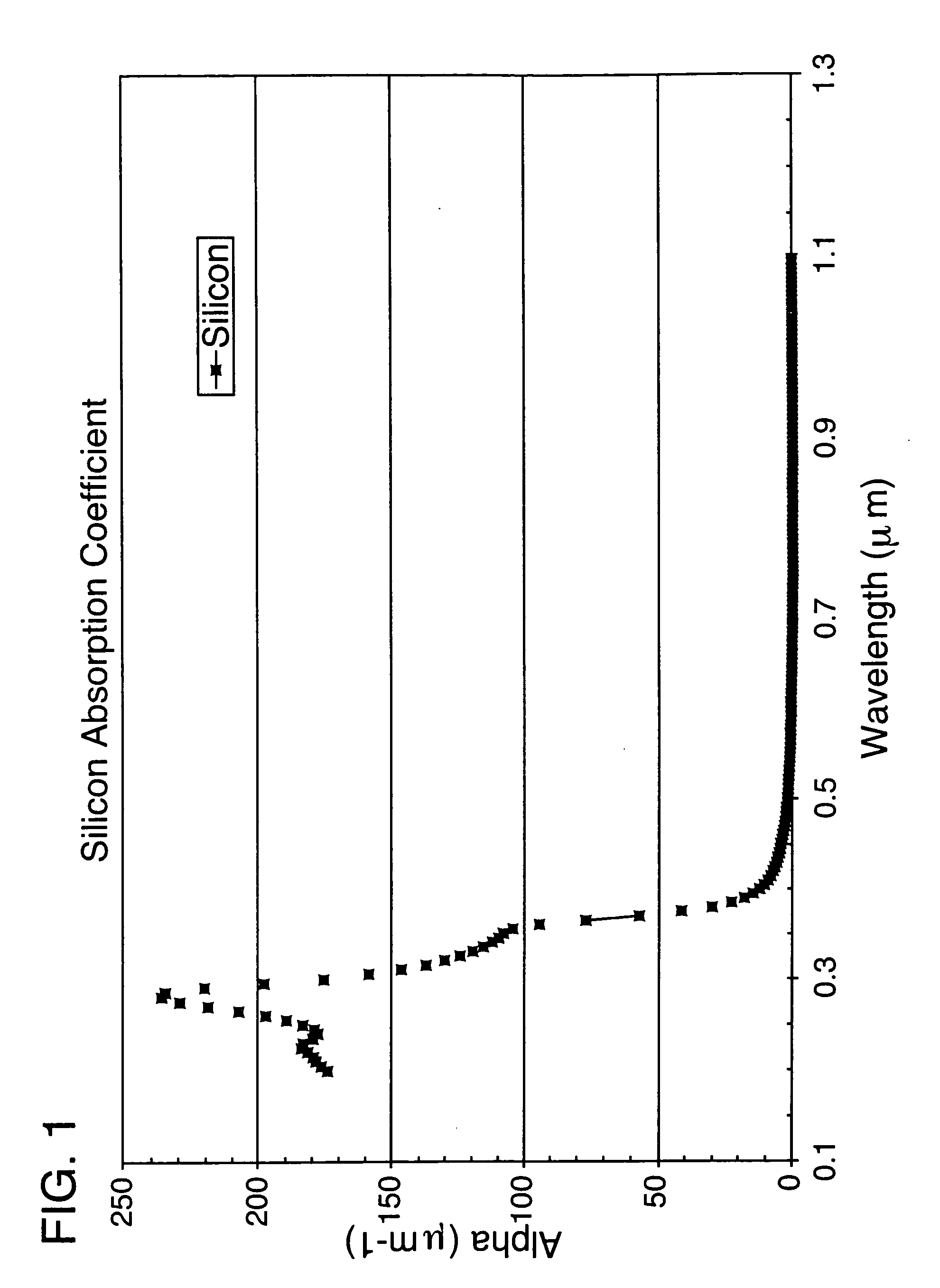
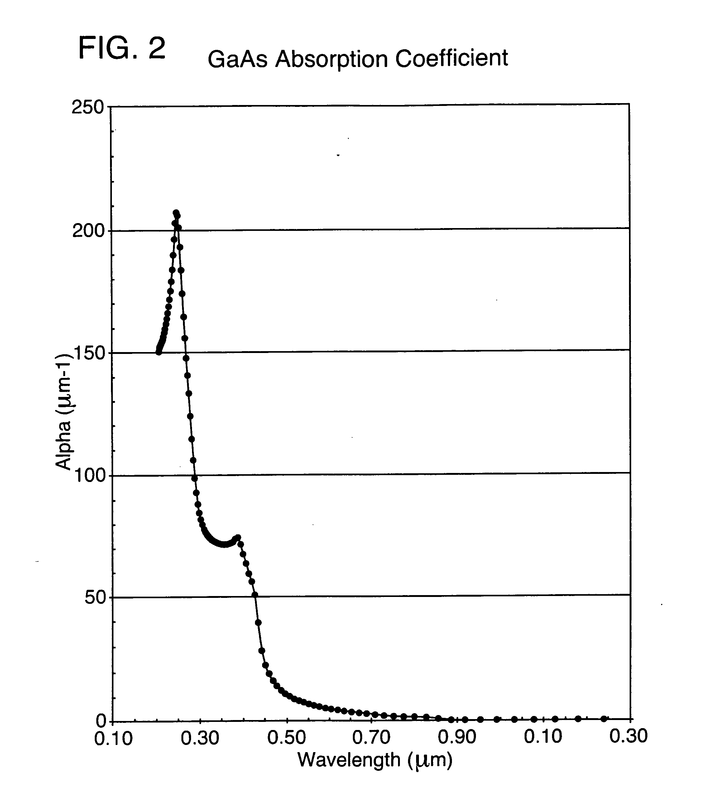
Semiconductor substrates, particularly silicon and gallium arsenide, present unique challenges for ultrafast laser fabrication. While these materials are fundamental to conventional electronics, their optical properties and heat dissipation characteristics require carefully optimized laser parameters to achieve precise modifications without collateral damage. Recent advances in laser pulse shaping and beam delivery have expanded the processing window for these materials.
Material selection must also consider the intended application environment of the embedded circuits. Factors such as operating temperature range, exposure to chemicals or radiation, mechanical stress, and required lifetime all influence material choice. For instance, aerospace applications may prioritize radiation hardness and thermal stability, while biomedical implants demand biocompatibility and long-term stability in physiological environments.
The interface properties between different materials in multilayer structures require particular attention. Thermal expansion coefficient mismatches can lead to delamination or stress-induced failures during thermal cycling. Adhesion promotion techniques and gradient interfaces have proven effective in mitigating these challenges, enabling more complex heterogeneous integration.
Emerging materials such as transparent ceramics, glass-ceramics, and specialized composites are expanding the material palette for ultrafast laser fabrication. These materials offer enhanced mechanical properties, higher temperature stability, or specific functional characteristics that may enable new applications beyond what conventional materials can support. Research into material-specific absorption mechanisms and modification thresholds continues to refine selection criteria and processing parameters.
Polymeric materials offer complementary advantages, including flexibility, lower cost, and ease of processing. Polyimides, polycarbonates, and certain photosensitive polymers demonstrate promising compatibility with ultrafast laser processing, though they generally exhibit lower damage thresholds compared to their glass counterparts. The integration of polymer-glass composites presents an emerging approach that combines the benefits of both material classes.
Semiconductor substrates, particularly silicon and gallium arsenide, present unique challenges for ultrafast laser fabrication. While these materials are fundamental to conventional electronics, their optical properties and heat dissipation characteristics require carefully optimized laser parameters to achieve precise modifications without collateral damage. Recent advances in laser pulse shaping and beam delivery have expanded the processing window for these materials.
Material selection must also consider the intended application environment of the embedded circuits. Factors such as operating temperature range, exposure to chemicals or radiation, mechanical stress, and required lifetime all influence material choice. For instance, aerospace applications may prioritize radiation hardness and thermal stability, while biomedical implants demand biocompatibility and long-term stability in physiological environments.
The interface properties between different materials in multilayer structures require particular attention. Thermal expansion coefficient mismatches can lead to delamination or stress-induced failures during thermal cycling. Adhesion promotion techniques and gradient interfaces have proven effective in mitigating these challenges, enabling more complex heterogeneous integration.
Emerging materials such as transparent ceramics, glass-ceramics, and specialized composites are expanding the material palette for ultrafast laser fabrication. These materials offer enhanced mechanical properties, higher temperature stability, or specific functional characteristics that may enable new applications beyond what conventional materials can support. Research into material-specific absorption mechanisms and modification thresholds continues to refine selection criteria and processing parameters.
Environmental Impact and Sustainability of Laser Fabrication Processes
Ultrafast laser fabrication of embedded circuits presents significant environmental considerations that must be evaluated within the broader context of sustainable manufacturing. Traditional circuit fabrication methods often involve chemical etching processes that generate substantial hazardous waste and require extensive water usage. In contrast, laser-based fabrication offers a potentially more environmentally friendly alternative by reducing chemical consumption and minimizing waste generation through precise material removal.
The energy efficiency of ultrafast laser systems represents a critical sustainability factor. Current systems typically operate at 10-30% wall-plug efficiency, with significant energy losses occurring during laser generation and beam delivery. Recent advancements in fiber laser technology have improved efficiency metrics, with some systems achieving up to 40% efficiency. However, the environmental benefits of these improvements must be weighed against the increased energy demands of higher pulse repetition rates in industrial applications.
Material utilization rates in ultrafast laser fabrication significantly outperform conventional subtractive manufacturing techniques. The precise nature of femtosecond laser processing enables material removal with micron-level accuracy, reducing waste by up to 80% compared to traditional circuit fabrication methods. Additionally, the ability to process materials in ambient conditions without vacuum requirements further reduces the environmental footprint of the manufacturing process.
Lifecycle assessment studies indicate that the environmental impact of ultrafast laser systems is heavily concentrated in the manufacturing and operational phases. The production of specialized optical components and precision positioning systems involves energy-intensive processes and rare earth elements. However, the extended operational lifespan of modern laser systems (typically 7-10 years) helps distribute this initial environmental cost over a longer productive period.
Waste management considerations for laser-fabricated embedded circuits present both challenges and opportunities. The ablation process generates particulate matter that requires appropriate filtration and collection systems. However, the composition of this waste is often less chemically complex than traditional etching residues, potentially simplifying disposal or recycling pathways. Some research facilities have implemented closed-loop material recovery systems that capture and repurpose up to 60% of ablated metals from certain fabrication processes.
Regulatory frameworks governing laser manufacturing processes continue to evolve, with increasing emphasis on energy consumption metrics and end-of-life product management. The European Union's Eco-design Directive and similar regulations in other regions are beginning to incorporate specific provisions for advanced manufacturing technologies, including ultrafast laser processing. Compliance with these emerging standards will likely become a significant factor in the commercial viability of laser-fabricated embedded circuits.
Unlock deeper insights with Patsnap Eureka Quick Research — get a full tech report to explore trends and direct your research. Try now!
Generate Your Research Report Instantly with AI Agent
Supercharge your innovation with Patsnap Eureka AI Agent Platform!