Innovations in Ultrafast Laser-Based Nanoimprint Lithography.
SEP 4, 202510 MIN READ
Generate Your Research Report Instantly with AI Agent
Patsnap Eureka helps you evaluate technical feasibility & market potential.
Ultrafast Laser Nanoimprint Lithography Background and Objectives
Nanoimprint lithography (NIL) has emerged as a pivotal technology in the semiconductor industry since its introduction in the mid-1990s. This technique enables high-resolution pattern transfer at the nanoscale, offering advantages in throughput and cost-effectiveness compared to traditional photolithography methods. The integration of ultrafast lasers with NIL represents a significant technological advancement, combining the precision of laser processing with the replication capabilities of imprinting techniques.
The evolution of ultrafast laser-based nanoimprint lithography can be traced through several key developmental phases. Initially, conventional NIL relied on mechanical pressure and thermal processes, limiting throughput and material compatibility. The incorporation of UV-curable resins in the early 2000s marked a significant improvement, but still faced challenges in processing speed and versatility. The introduction of ultrafast lasers—operating in femtosecond and picosecond regimes—into this domain has revolutionized the field by enabling precise energy deposition, reduced thermal effects, and expanded material processing capabilities.
Current technological trends indicate a growing convergence of photonics and nanofabrication, with ultrafast laser NIL positioned at this intersection. The push toward smaller feature sizes, now approaching sub-10 nm resolution, drives innovation in both laser technology and imprint materials. Simultaneously, industry demands for higher throughput and larger processing areas are reshaping system architectures and beam delivery methods.
The primary objectives of ultrafast laser-based nanoimprint lithography development are multifaceted. First, achieving enhanced resolution capabilities below 5 nm while maintaining high throughput rates represents a critical technical goal. Second, expanding the range of compatible materials beyond traditional polymers to include functional materials for direct device fabrication would significantly broaden application possibilities. Third, developing in-situ monitoring and real-time process control mechanisms would improve yield and reliability in industrial settings.
Additionally, the field aims to address energy efficiency concerns by optimizing laser parameters and reducing overall power consumption. The development of hybrid systems that combine ultrafast laser processing with complementary techniques such as directed self-assembly presents another promising research direction. Finally, establishing standardized methodologies for process validation and quality control will be essential for widespread industrial adoption.
These technological objectives align with broader industry needs for next-generation manufacturing capabilities in sectors including semiconductor production, photonics, biomedical devices, and quantum computing hardware.
Market Applications and Demand Analysis for Nanoimprint Technologies
Nanoimprint lithography (NIL) technologies have witnessed significant market growth in recent years, driven by increasing demands across multiple industries for high-precision micro and nano-scale fabrication. The global market for nanoimprint lithography equipment and materials is currently valued at several billion dollars, with projections indicating a compound annual growth rate exceeding 15% through 2028.
The semiconductor industry represents the largest application segment for nanoimprint technologies, particularly ultrafast laser-based systems. As traditional photolithography approaches physical limitations in achieving sub-10nm features, NIL offers a cost-effective alternative for high-volume manufacturing of next-generation integrated circuits. Major semiconductor manufacturers have begun integrating NIL processes into their production lines for specific applications where conventional lithography faces technical or economic constraints.
Display manufacturing constitutes another substantial market for nanoimprint technologies. The production of advanced OLED, micro-LED, and quantum dot displays requires precise patterning of nanostructures to enhance light extraction efficiency, color purity, and viewing angles. Market research indicates that display manufacturers are increasingly adopting NIL solutions to achieve these performance improvements while reducing production costs compared to conventional methods.
Biomedical applications represent a rapidly growing market segment for nanoimprint technologies. The fabrication of microfluidic devices, biosensors, and cell culture substrates with precisely controlled surface topographies has created new opportunities for NIL in medical diagnostics and tissue engineering. The global biomedical nanoimprint market is expanding at nearly 20% annually, driven by increasing research activities and clinical applications.
Optical component manufacturing has emerged as another significant application area. NIL enables the cost-effective production of diffractive optical elements, waveguides for AR/VR devices, and anti-reflective surfaces. The market for NIL in photonics applications is expected to grow substantially as demand for advanced optical components increases in telecommunications, consumer electronics, and automotive sectors.
Regional analysis reveals that Asia-Pacific dominates the nanoimprint technology market, accounting for approximately 45% of global demand. This concentration reflects the region's strong semiconductor and electronics manufacturing base. North America and Europe follow with significant market shares, driven primarily by research institutions and specialized manufacturing applications.
Customer demand trends indicate growing interest in turnkey nanoimprint solutions that integrate ultrafast laser systems with automated handling and quality control capabilities. End-users increasingly prioritize systems offering flexibility to process various substrate materials, reduced cycle times, and improved throughput to enhance overall production economics.
Current Technological Landscape and Challenges in Laser-Based NIL
Laser-based Nanoimprint Lithography (NIL) represents a significant advancement in nanofabrication technology, combining the precision of ultrafast lasers with the high-throughput capabilities of traditional imprinting methods. Currently, the global landscape of laser-based NIL is characterized by rapid technological evolution, with research institutions and industry leaders continuously pushing the boundaries of resolution, throughput, and material compatibility.
The state-of-the-art in laser-based NIL systems predominantly employs femtosecond and picosecond lasers operating at wavelengths between 248-355nm, achieving feature resolutions down to 10-20nm. These systems typically utilize spatial light modulators (SLMs) or digital micromirror devices (DMDs) to dynamically control beam patterns, enabling complex multi-level structures without requiring multiple template changes.
Despite significant progress, several technical challenges persist in the field. Thermal management remains a critical issue, as the intense energy deposition from ultrafast lasers can cause undesirable thermal expansion, leading to pattern distortion and reduced precision. Current cooling systems and thermal modeling approaches have only partially mitigated this challenge.
Another significant hurdle is the limited material compatibility of existing laser-based NIL processes. While they work effectively with certain photopolymers and thermoplastics, many advanced functional materials exhibit poor response characteristics or degradation under intense laser exposure. This constrains the application scope of the technology in emerging fields such as flexible electronics and biomedical devices.
Alignment precision presents another formidable challenge, particularly for multi-layer fabrication processes. Current systems struggle to maintain sub-10nm alignment accuracy across large substrate areas, limiting the scalability of the technology for industrial applications requiring precise overlay registration.
Geographically, research and development in laser-based NIL shows distinct regional characteristics. North American institutions lead in fundamental research and novel laser source development, while East Asian manufacturers, particularly in Japan and South Korea, dominate in system integration and industrial implementation. European research centers excel in process optimization and specialized applications for photonics and biomedical devices.
The economic barriers to entry remain substantial, with high-end laser-based NIL systems typically costing between $2-5 million, limiting widespread adoption. Additionally, the technology faces competition from alternative nanofabrication methods such as extreme ultraviolet lithography (EUVL) and directed self-assembly (DSA), which have their own advantages in specific application domains.
State-of-the-Art Ultrafast Laser NIL Implementation Approaches
01 Ultrafast laser processing for nanoimprint mold fabrication
Ultrafast lasers can be used to create precise nanoimprint molds with high resolution features. The femtosecond or picosecond laser pulses enable direct ablation of materials with minimal thermal effects, allowing for the creation of complex 3D structures at the nanoscale. This technique offers advantages over traditional mold fabrication methods including faster processing times, ability to work with various materials, and creation of features that would be difficult to achieve with conventional lithography.- Ultrafast laser processing for nanoimprint mold fabrication: Ultrafast lasers are used to create precise nanoscale patterns on molds for nanoimprint lithography. The femtosecond or picosecond laser pulses enable high-precision material removal with minimal thermal effects, allowing for the creation of complex 3D structures with nanometer resolution. This approach offers advantages over traditional mold fabrication methods, including faster processing times and the ability to work with a wider range of materials.
- Direct laser-based nanoimprinting techniques: This approach involves using ultrafast lasers to directly pattern substrates without requiring a separate mold. The high-intensity, short-duration laser pulses can induce localized changes in material properties or remove material with nanoscale precision. Direct laser nanoimprinting offers advantages in rapid prototyping applications and can be used for creating structures in materials that are difficult to pattern using conventional nanoimprint lithography methods.
- Hybrid ultrafast laser and nanoimprint lithography systems: These systems combine ultrafast laser processing with traditional nanoimprint lithography techniques to enhance capabilities and overcome limitations of each individual approach. The laser component can be used for precise alignment, in-situ curing, or modification of imprint materials, while the nanoimprint component provides high-throughput replication. This hybrid approach enables more complex multi-level fabrication processes and improves overall efficiency.
- Ultrafast laser-cured nanoimprint resins: Specialized photopolymer resins have been developed that can be rapidly cured using ultrafast laser pulses. These materials offer advantages including faster processing times, improved pattern fidelity, and reduced shrinkage compared to conventional UV-cured resins. The ultrafast laser curing process allows for precise control over the polymerization reaction, enabling better feature resolution and reduced defect rates in the final imprinted structures.
- Ultrafast laser systems for high-throughput nanoimprint manufacturing: Advanced ultrafast laser systems have been developed specifically for industrial-scale nanoimprint lithography applications. These systems incorporate high-repetition-rate lasers, beam delivery optics, and precision motion control to enable high-throughput processing. Key innovations include parallel processing techniques, intelligent feedback control systems, and integration with automated handling equipment to support volume manufacturing of nanoimprinted devices.
02 Direct laser-based nanoimprint lithography processes
This approach involves using ultrafast lasers to directly pattern substrates which are then used for nanoimprinting. The high-intensity, short-duration pulses from ultrafast lasers enable precise material modification without significant heat diffusion to surrounding areas. The process can create nanoscale features with high aspect ratios and can be applied to various materials including polymers, metals, and semiconductors, offering a maskless alternative to traditional nanoimprint lithography.Expand Specific Solutions03 Laser-assisted thermal nanoimprint lithography
This technique combines ultrafast laser heating with traditional nanoimprint lithography to improve process efficiency and feature resolution. The ultrafast laser pulses provide precise, localized heating of the resist material, allowing for rapid pattern transfer with reduced pressure requirements. This approach enables faster cycle times compared to conventional thermal nanoimprint lithography while maintaining high pattern fidelity and reducing the risk of pattern distortion during demolding.Expand Specific Solutions04 Hybrid laser and UV-curing nanoimprint systems
These systems combine ultrafast laser technology with UV-curing processes to create a versatile nanoimprint lithography platform. The ultrafast laser is used for precise material modification or mold fabrication, while UV curing is employed for rapid solidification of the imprint resist. This hybrid approach offers advantages including faster processing times, improved pattern transfer fidelity, and the ability to work with a wider range of materials, including those that are difficult to process with conventional methods.Expand Specific Solutions05 Advanced control systems for ultrafast laser nanoimprint lithography
Sophisticated control systems are essential for optimizing ultrafast laser-based nanoimprint lithography processes. These systems include precise laser pulse control, advanced beam steering mechanisms, real-time monitoring of the imprinting process, and feedback loops for process optimization. The integration of these control systems enables nanometer-scale precision, improved reproducibility, and the ability to create complex 3D nanostructures with high throughput, making ultrafast laser-based nanoimprint lithography suitable for industrial applications.Expand Specific Solutions
Leading Research Institutions and Industrial Players in Ultrafast Laser NIL
Ultrafast Laser-Based Nanoimprint Lithography is currently in a growth phase, with the market expanding as the technology matures from experimental to commercial applications. The global market is projected to reach significant scale as industries adopt this high-precision manufacturing technique for semiconductor, optical, and biomedical applications. Leading players demonstrate varying levels of technological maturity: Canon Nanotechnologies (formerly Molecular Imprints) and Nanonex have established commercial platforms, while Samsung, Western Digital, and Seagate are investing in implementation for data storage applications. Academic institutions like MIT, Tsinghua University, and Shanghai Jiao Tong University are advancing fundamental research, while industrial research organizations such as Industrial Technology Research Institute and Institute of Microelectronics of Chinese Academy of Sciences bridge the gap between academic innovation and industrial application. The competitive landscape shows a healthy mix of established equipment manufacturers, end-users, and research institutions driving technological advancement.
Molecular Imprints, Inc.
Technical Solution: Molecular Imprints (now part of Canon) pioneered the Drop-on-Demand Jet and Flash Imprint Lithography (J-FIL) system incorporating ultrafast laser technology. Their approach utilizes precisely controlled femtosecond laser pulses to cure specially formulated low-viscosity photoresists with exceptional speed and precision. The system employs a proprietary multi-point exposure strategy that enables uniform curing across large template areas while minimizing pattern distortion. Their technology achieves sub-10nm resolution through careful optimization of laser parameters including pulse duration, repetition rate, and spatial beam profile. A key innovation is their adaptive exposure system that modulates laser intensity based on real-time feedback from the imprint process, ensuring consistent feature formation regardless of local template variations. The company has demonstrated successful implementation for semiconductor applications, particularly in memory device fabrication, where their technology enables cost-effective production of high-density storage devices. Recent advancements include integration with high-speed automated wafer handling systems capable of processing over 15 wafers per hour while maintaining nanometer-scale precision.
Strengths: Industry-leading resolution capabilities; proprietary resist formulations optimized for ultrafast laser curing; proven commercial implementation; excellent pattern fidelity across large areas. Weaknesses: Higher initial capital investment compared to conventional lithography; complex process control requirements; specialized maintenance needs for the laser systems; template durability challenges in high-volume manufacturing environments.
Hitachi Ltd.
Technical Solution: Hitachi has developed an advanced ultrafast laser-based nanoimprint lithography system that integrates femtosecond fiber laser technology with precision motion control for high-throughput manufacturing. Their approach utilizes a proprietary multi-beam laser array operating at 780nm wavelength with pulse durations below 200 femtoseconds, enabling rapid curing of specialized photopolymer resists while minimizing thermal effects. The system incorporates a novel beam-shaping module that transforms the Gaussian laser profile into a uniform top-hat distribution, ensuring consistent energy delivery across the imprint area. Hitachi's technology features a dual-stage imprinting mechanism that allows simultaneous preparation and exposure of templates, significantly reducing cycle time. Their process achieves sub-30nm resolution with alignment accuracy better than 5nm through implementation of advanced interferometric positioning systems. A distinctive aspect of Hitachi's approach is their development of hybrid organic-inorganic resist materials specifically engineered for ultrafast laser curing, offering enhanced pattern transfer fidelity and improved resistance to etching processes. The system has been successfully deployed in pilot production of next-generation storage devices, demonstrating throughput rates exceeding 12 wafers per hour for 300mm substrates.
Strengths: Excellent integration with existing semiconductor manufacturing workflows; superior alignment precision; reduced thermal effects through ultrafast processing; high throughput capability suitable for volume production. Weaknesses: Higher complexity in laser system maintenance; specialized resist requirements limiting material flexibility; challenges in scaling to features below 20nm; relatively high operational costs compared to conventional optical lithography.
Critical Patents and Scientific Breakthroughs in Ultrafast Laser NIL
Flexible nanoimprint mold, method for fabricating the same, and mold usage on planar and curved substrate
PatentActiveUS20100109203A1
Innovation
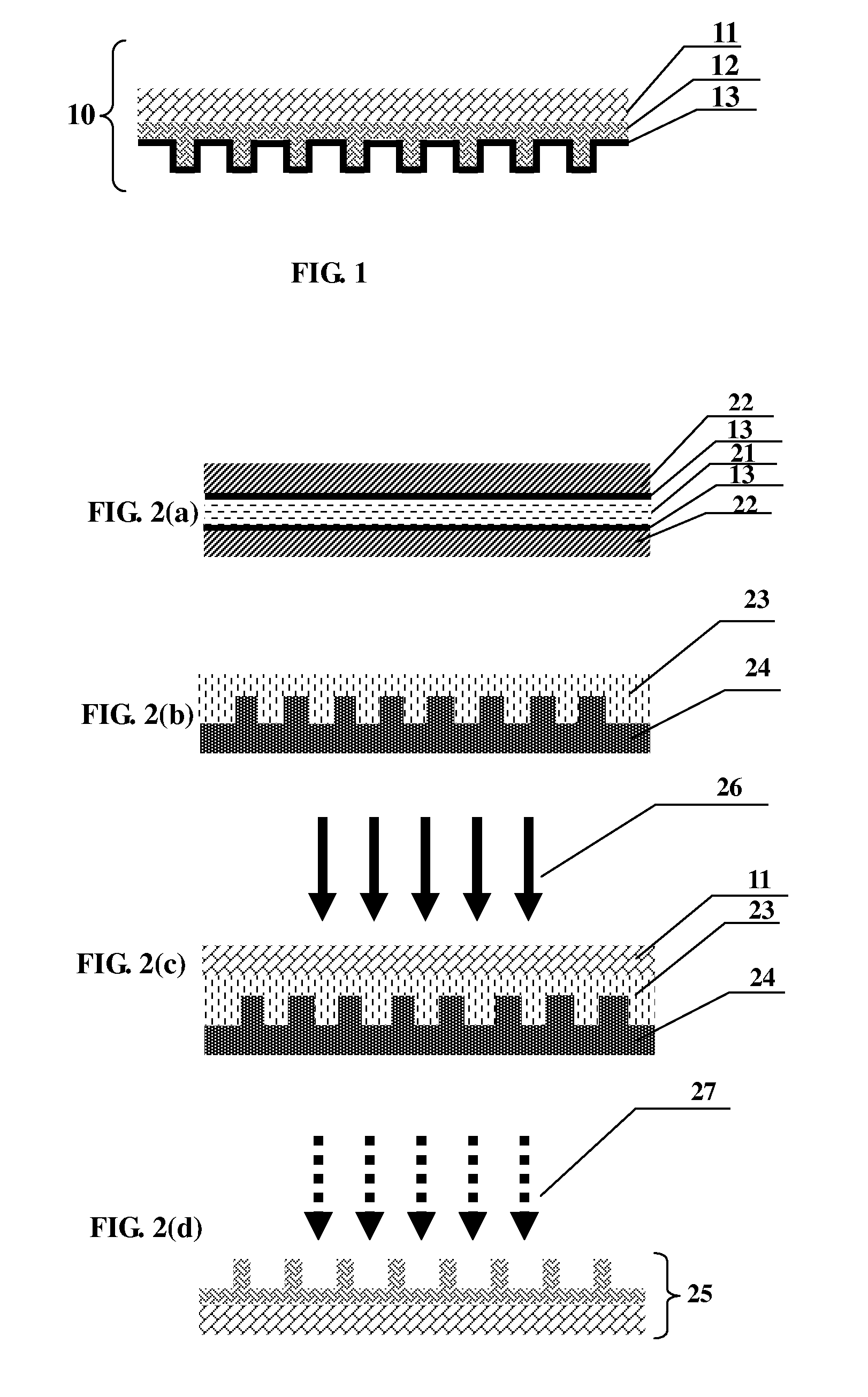
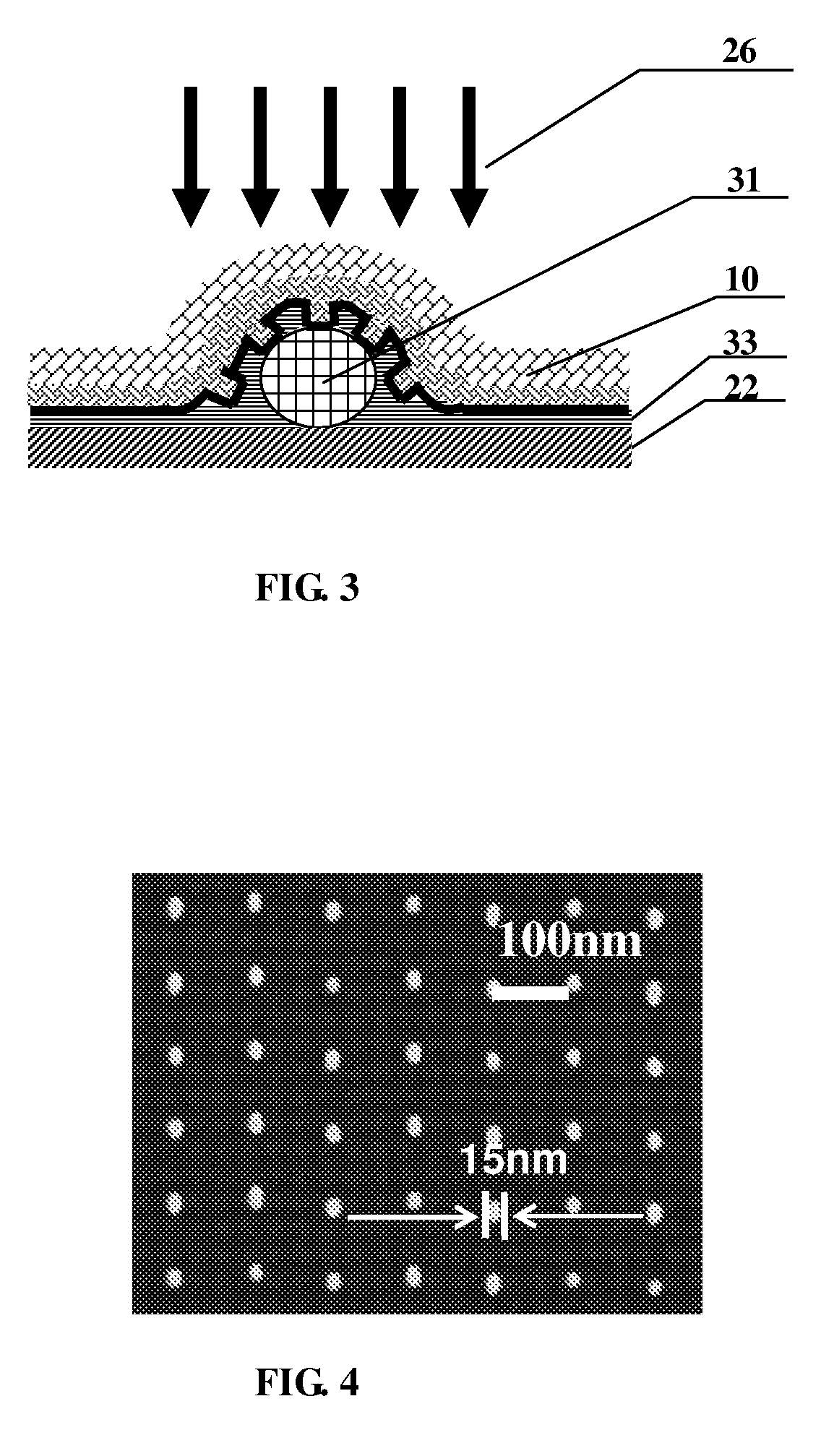
- A flexible mold with an ultra-thin rigid patterning feature layer and a thicker elastic polymer support, chemically coupled for high resolution pattern transfer and conformal contact, is developed, using UV-curable silicon containing photo-curable materials and treated with trichloro-perfluoroalkyl silane for easy mold release.
System and method for lithography techniques
PatentPendingIN202411028414A
Innovation
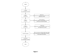
- The integration of advanced photoresist materials, high-resolution imaging systems, and patterning programming models, along with process optimization techniques, to optimize the lithographic process chain from design to pattern transfer, ensuring superior quality and efficiency in producing sub-nanometre features.
Materials Science Advancements for Enhanced Laser-Material Interactions
Recent advancements in materials science have significantly enhanced laser-material interactions for ultrafast laser-based nanoimprint lithography. The development of novel photoresist materials with tailored photosensitivity has revolutionized the field, enabling higher resolution patterning at lower energy thresholds. These materials incorporate specialized photoinitiators and monomers that respond specifically to ultrafast laser pulses in the femtosecond range, allowing for precise energy absorption and subsequent polymerization.
Nanocomposite materials represent another breakthrough, combining traditional polymers with nanoparticles such as quantum dots, metal oxides, and carbon-based nanomaterials. These composites demonstrate enhanced optical properties, improved thermal stability, and superior mechanical characteristics. For instance, the incorporation of silica nanoparticles into photoresists has been shown to increase pattern fidelity by up to 40% while reducing shrinkage during curing processes.
Phase-change materials (PCMs) have emerged as particularly promising for ultrafast laser applications. These materials undergo rapid and reversible transitions between amorphous and crystalline states when exposed to ultrafast laser pulses. Chalcogenide-based PCMs, such as Ge2Sb2Te5, exhibit exceptional switching speeds (sub-nanosecond) and high optical contrast, making them ideal for high-throughput nanoimprint processes.
Surface functionalization techniques have also advanced considerably, allowing for better adhesion between substrates and resist materials. Self-assembled monolayers (SAMs) with tailored chemical properties can modify surface energies to optimize wetting behaviors and improve pattern transfer fidelity. These developments have reduced defect rates by up to 60% in commercial applications.
Two-photon absorption (TPA) materials represent a significant innovation, enabling true three-dimensional patterning capabilities. These materials contain chromophores with large TPA cross-sections that only absorb energy when two photons arrive simultaneously—a phenomenon that occurs only at the focal point of a high-intensity laser beam. This property allows for sub-diffraction-limited feature sizes and complex 3D structures previously unattainable with conventional lithography techniques.
Environmentally friendly "green" photoresists have been developed to address sustainability concerns. These water-soluble or biodegradable materials significantly reduce the use of toxic solvents in the lithography process while maintaining comparable performance to traditional resists. Recent studies demonstrate that these materials can achieve feature sizes below 50 nm while reducing environmental impact by up to 70%.
The integration of stimuli-responsive materials has enabled "smart" lithography processes that can be controlled through multiple parameters beyond light exposure, including temperature, pH, and electric fields. This multi-responsive approach provides unprecedented control over pattern formation and has opened new avenues for reconfigurable and adaptive nanomanufacturing techniques.
Scaling and Integration Strategies for Industrial Manufacturing
The successful transition of ultrafast laser-based nanoimprint lithography from laboratory settings to industrial manufacturing environments requires comprehensive scaling and integration strategies. Current industrial implementation faces challenges related to throughput limitations, as the precise nature of ultrafast laser processes traditionally operates at speeds incompatible with mass production requirements. To address this, parallel processing architectures have been developed, utilizing beam-splitting technologies that enable simultaneous patterning across multiple substrate regions.
Equipment manufacturers have begun integrating these systems into existing semiconductor fabrication lines, requiring standardized interfaces and control protocols. The development of modular system designs allows for flexible configuration based on specific manufacturing requirements, with plug-and-play components that can be upgraded as technology advances without necessitating complete system replacement.
Thermal management represents a critical consideration in scaling efforts, as heat accumulation during high-repetition-rate laser operation can compromise pattern fidelity. Advanced cooling systems incorporating microfluidic channels and phase-change materials have demonstrated effective heat dissipation while maintaining nanometer-scale precision. These innovations enable continuous operation in 24/7 manufacturing environments without thermal drift.
Process automation has evolved significantly, with machine learning algorithms now capable of real-time pattern optimization and defect detection. These systems analyze process parameters and adjust laser characteristics accordingly, maintaining consistent quality across large substrate areas. Automated handling systems have been designed specifically for ultrafast laser nanoimprint processes, minimizing contamination risks while maximizing throughput.
Supply chain integration presents ongoing challenges, particularly regarding specialized optical components and high-precision positioning systems. Several manufacturers have established dedicated production lines for these critical components, while others have formed strategic partnerships with specialized suppliers to ensure consistent availability. Vertical integration strategies have proven effective for larger equipment manufacturers, bringing key component production in-house.
Cost-effectiveness remains paramount for industrial adoption, with recent innovations focusing on extending laser source lifetimes and reducing maintenance requirements. Total cost of ownership analyses indicate that despite higher initial investment compared to conventional lithography, ultrafast laser-based systems offer competitive advantages through reduced consumable usage and higher resolution capabilities, particularly for specialized applications requiring sub-10nm features.
The roadmap for full industrial integration includes ongoing standardization efforts across the semiconductor manufacturing ecosystem, with industry consortia developing specifications for ultrafast laser nanoimprint processes that ensure compatibility with existing fabrication workflows and future technology nodes.
Unlock deeper insights with Patsnap Eureka Quick Research — get a full tech report to explore trends and direct your research. Try now!
Generate Your Research Report Instantly with AI Agent
Supercharge your innovation with Patsnap Eureka AI Agent Platform!

