Efficiency Gains In Variable Frequency Drives Using GaN HEMTs
SEP 8, 20259 MIN READ
Generate Your Research Report Instantly with AI Agent
Patsnap Eureka helps you evaluate technical feasibility & market potential.
GaN HEMT VFD Technology Background and Objectives
Gallium Nitride High Electron Mobility Transistors (GaN HEMTs) represent a revolutionary advancement in semiconductor technology that has evolved significantly over the past two decades. Initially developed for military and aerospace applications in the early 2000s, these wide-bandgap semiconductors have gradually transitioned into commercial power electronics applications. The evolution of GaN technology has been marked by continuous improvements in material quality, device design, and manufacturing processes, leading to enhanced performance characteristics and reduced costs.
Variable Frequency Drives (VFDs), which control AC motor speed and torque by varying motor input frequency and voltage, have traditionally relied on silicon-based power devices such as IGBTs and MOSFETs. However, these conventional technologies face inherent limitations in switching frequency, power density, and thermal performance that constrain the overall efficiency and size of VFD systems.
The integration of GaN HEMTs into VFD applications represents a convergence of two mature technologies with the potential to address critical industry challenges. The superior material properties of GaN, including higher breakdown voltage, faster switching speeds, and lower on-resistance, offer significant advantages over silicon-based alternatives. These properties enable VFDs to operate at higher frequencies with reduced switching losses, ultimately leading to smaller passive components and increased power density.
Current technological trends indicate a growing interest in GaN-based power electronics across various industries, with particular emphasis on applications requiring high efficiency and compact form factors. The compound annual growth rate for GaN power devices is projected to exceed 30% through 2026, signaling strong market confidence in this technology's potential.
The primary technical objectives for GaN HEMT implementation in VFDs include achieving efficiency improvements of 2-3% over conventional silicon-based solutions, reducing system size by 30-40% through higher frequency operation, enhancing thermal performance to increase reliability in harsh industrial environments, and developing cost-effective manufacturing processes to enable broader market adoption.
Additionally, researchers aim to address specific challenges related to GaN technology, such as dynamic on-resistance, gate reliability, and packaging innovations that can fully leverage the inherent advantages of these devices. The development of specialized gate drivers and control algorithms optimized for the unique switching characteristics of GaN HEMTs represents another critical objective in this technological evolution.
As industrial systems face increasing pressure to improve energy efficiency and reduce physical footprint, the successful integration of GaN HEMTs into VFD applications could establish a new performance benchmark for motor drive systems across manufacturing, HVAC, renewable energy, and electric vehicle charging infrastructure.
Market Analysis for GaN-based Variable Frequency Drives
The global market for GaN-based Variable Frequency Drives (VFDs) is experiencing significant growth, driven by increasing demand for energy-efficient motor control systems across various industries. Current market valuations indicate that the GaN power device market is projected to reach approximately 1.75 billion USD by 2026, with VFD applications representing a substantial segment of this growth trajectory.
Industrial automation remains the primary application sector, accounting for roughly 35% of the total market share. This dominance stems from the manufacturing sector's continuous push toward energy efficiency and operational cost reduction. The HVAC industry follows closely, representing about 28% of market demand, as building energy management becomes increasingly critical in commercial and residential applications.
Regional analysis reveals that Asia-Pacific currently leads the market with approximately 40% share, primarily due to rapid industrialization in China, Japan, and South Korea. North America and Europe collectively account for about 45% of the market, with particularly strong adoption in renewable energy integration and industrial automation sectors.
The market is experiencing a compound annual growth rate of approximately 22%, significantly outpacing traditional silicon-based VFD solutions which grow at roughly 5-7% annually. This accelerated growth is directly attributable to the superior performance characteristics of GaN HEMTs in high-frequency switching applications.
Customer segmentation analysis indicates that large industrial enterprises currently constitute about 60% of end-users, while small and medium enterprises represent an emerging growth segment with increasing adoption rates of 30% year-over-year. This shift is primarily driven by decreasing component costs and greater awareness of long-term operational savings.
Price sensitivity analysis reveals that despite higher initial costs (typically 30-40% premium over silicon-based alternatives), the total cost of ownership for GaN-based VFDs becomes favorable within 2-3 years of operation due to energy savings of 15-20% and reduced maintenance requirements.
Competitive landscape assessment identifies three distinct market tiers: established power electronics giants incorporating GaN technology into their product lines; specialized GaN semiconductor manufacturers forming strategic partnerships with VFD producers; and emerging startups focused exclusively on GaN-based motor control solutions. Market concentration remains moderate with the top five players controlling approximately 55% of market share.
Future market projections indicate potential disruption in traditional industrial motor control paradigms, with GaN-based VFDs potentially capturing up to 40% of the total VFD market by 2030, representing a significant shift from the current 8-10% market penetration.
Current Challenges in GaN HEMT Implementation for VFDs
Despite the promising advantages of GaN HEMTs in Variable Frequency Drive applications, several significant challenges currently impede their widespread implementation. The thermal management of GaN devices presents a primary obstacle, as these components generate substantial heat during high-frequency switching operations. The thermal conductivity limitations of GaN substrates, particularly in lateral device structures, create hotspots that can compromise reliability and performance if not adequately addressed through advanced cooling solutions.
Cost factors remain a substantial barrier to mass adoption, with GaN HEMTs typically commanding a 3-5x price premium over traditional silicon alternatives. This cost differential stems from smaller production volumes, specialized manufacturing processes, and the relatively immature supply chain for GaN power devices. While economies of scale are gradually improving this situation, the current price point restricts GaN implementation primarily to premium VFD applications where performance benefits can justify the additional expense.
Reliability concerns also persist within the industry. Although significant progress has been made, GaN HEMTs still face challenges related to dynamic RDS(on) degradation under certain operating conditions, gate reliability issues, and long-term stability questions that require further investigation. The limited field deployment history compared to silicon technologies creates hesitation among conservative industrial customers who prioritize proven reliability over cutting-edge performance.
Integration complexities present another significant hurdle. GaN HEMTs exhibit faster switching speeds and lower gate charge than silicon devices, necessitating careful circuit design to manage parasitic inductances and prevent voltage overshoots or ringing. Additionally, gate driver requirements differ substantially from traditional silicon MOSFETs, often requiring specialized components and protection mechanisms to ensure safe and efficient operation.
The regulatory and standardization landscape remains underdeveloped for GaN technology in power applications. The absence of comprehensive standards specifically addressing GaN HEMT implementation in VFDs creates uncertainty regarding qualification requirements, testing protocols, and safety certifications. This regulatory gap slows adoption in industries with stringent compliance requirements.
Manufacturing scalability challenges persist as well. Current GaN HEMT production processes have not yet achieved the maturity and yield consistency of silicon manufacturing. The specialized epitaxial growth techniques, substrate materials, and processing steps introduce variability that can affect device performance characteristics across production batches, complicating quality control and system design.
Knowledge gaps among engineers and system designers further impede adoption. The unique characteristics of GaN HEMTs require different design approaches and considerations compared to traditional silicon-based systems. The limited availability of comprehensive design resources, application notes, and practical implementation guidelines creates a steep learning curve for engineering teams exploring GaN technology for VFD applications.
Technical Solutions for GaN HEMT Integration in VFDs
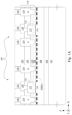
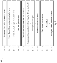
01 Device structure optimization for improved efficiency
Various structural modifications in GaN HEMTs can significantly enhance their efficiency. These include optimized gate designs, improved channel structures, and novel substrate configurations. By carefully engineering the device architecture, power losses can be minimized while maximizing electron mobility in the 2DEG channel. These structural innovations help reduce on-resistance and parasitic capacitances, leading to higher switching speeds and better overall power conversion efficiency.- Device structure optimization for improved efficiency: Optimizing the structure of GaN HEMTs can significantly improve their efficiency. This includes modifications to the gate design, channel structure, and substrate materials. Advanced gate structures like recessed gates or field plates can reduce gate leakage and improve electron confinement. Optimized channel designs with appropriate buffer layers help minimize current collapse and enhance carrier mobility, leading to better power efficiency and performance at high frequencies.
- Thermal management techniques: Effective thermal management is crucial for maintaining high efficiency in GaN HEMTs. Various approaches include improved heat dissipation through advanced packaging, integration of thermal vias, and use of high thermal conductivity materials. Diamond substrates or heat spreaders can significantly enhance heat extraction from the active device region. These thermal management techniques prevent performance degradation at high power levels and extend device lifetime by reducing thermal stress.
- Surface passivation and interface engineering: Surface passivation and interface engineering play critical roles in enhancing GaN HEMT efficiency. Proper passivation layers reduce surface traps and current collapse effects that degrade device performance. Advanced dielectric materials and deposition techniques can minimize interface states between the semiconductor and insulator layers. Optimized passivation strategies help maintain high electron mobility in the two-dimensional electron gas (2DEG) channel while reducing parasitic effects that limit efficiency.
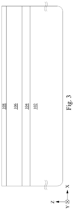
- Novel material systems and epitaxial growth techniques: Advanced material systems and epitaxial growth techniques can significantly improve GaN HEMT efficiency. This includes the development of high-quality AlGaN/GaN heterostructures with precise control over composition and thickness. Innovations in metal-organic chemical vapor deposition (MOCVD) and molecular beam epitaxy (MBE) processes enable the growth of high-quality epitaxial layers with reduced defect densities. Integration of novel materials like InAlN barrier layers or GaN-on-diamond structures can further enhance device performance and efficiency.
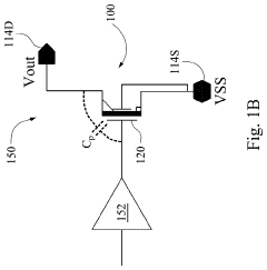
- Power conversion circuit design and system integration: Optimizing power conversion circuit design and system integration is essential for maximizing the efficiency benefits of GaN HEMTs. This includes developing specialized driver circuits that can fully utilize the high-speed switching capabilities of GaN devices. Advanced circuit topologies like soft-switching techniques reduce switching losses. Integration approaches that minimize parasitic inductances and capacitances in the circuit layout help achieve higher operating frequencies and improved power density, resulting in more efficient power conversion systems.
02 Advanced materials and epitaxial techniques
The efficiency of GaN HEMTs is heavily dependent on the quality of materials and epitaxial growth techniques used. Innovations in buffer layer compositions, barrier materials, and surface passivation technologies have led to reduced defect densities and improved carrier confinement. Advanced epitaxial growth methods enable precise control over layer thicknesses and interfaces, resulting in enhanced electron mobility and reduced current collapse phenomena, ultimately improving the power handling capability and efficiency of these devices.Expand Specific Solutions03 Thermal management solutions
Effective thermal management is crucial for maintaining high efficiency in GaN HEMTs, as these devices can generate significant heat during operation. Various approaches include innovative heat sink designs, integration of thermal vias, diamond heat spreaders, and optimized packaging techniques. These solutions help dissipate heat more effectively, preventing performance degradation at high power levels and extending device lifetime while maintaining optimal efficiency across a wide operating temperature range.Expand Specific Solutions04 Gate drive and circuit integration techniques
Advanced gate drive techniques and circuit integration approaches significantly impact GaN HEMT efficiency. Optimized gate drivers with precise timing control, appropriate voltage levels, and fast switching capabilities help minimize switching losses. Integration of gate drivers with protection circuits, level shifters, and control logic on the same die or package reduces parasitic inductances and improves switching performance. These innovations enable GaN HEMTs to operate closer to their theoretical efficiency limits in practical power conversion applications.Expand Specific Solutions05 Reliability enhancement methods
Maintaining high efficiency over the device lifetime requires addressing reliability challenges in GaN HEMTs. Various approaches include improved passivation techniques to mitigate current collapse, field plate structures to manage peak electric fields, and specialized edge termination designs. Advanced stress testing methodologies help identify failure mechanisms, while novel processing techniques reduce defect formation. These reliability enhancements ensure that the high efficiency of GaN HEMTs is maintained throughout their operational lifetime under various environmental and electrical stress conditions.Expand Specific Solutions
Key Manufacturers and Competitors in GaN Power Electronics
The GaN HEMT-based variable frequency drive market is experiencing rapid growth in the early commercialization phase, with an estimated market size of $1.2-1.5 billion and projected CAGR of 25-30% through 2028. Leading players include established semiconductor manufacturers like Wolfspeed, GaN Systems, and MACOM Technology, who are developing advanced GaN-on-Si and GaN-on-SiC technologies. Research institutions such as IMEC and universities (Peking, Fudan) are collaborating with industry partners to overcome technical challenges in thermal management and reliability. Companies like Innoscience and Taiwan Semiconductor are scaling production capabilities, while system integrators including Mitsubishi Electric are incorporating GaN HEMTs into commercial VFD products, demonstrating efficiency improvements of 15-30% over silicon-based solutions.
Wolfspeed, Inc.
Technical Solution: Wolfspeed's GaN HEMT technology for variable frequency drives (VFDs) centers on their proprietary 650V GaN-on-SiC platform, which achieves switching frequencies up to 100kHz with efficiency exceeding 98%. Their solution integrates advanced gate driver technology with optimized packaging to minimize parasitic inductance, crucial for high-frequency operation. Wolfspeed's implementation features a two-level topology with synchronous rectification that reduces switching losses by approximately 40% compared to silicon IGBTs. Their thermal management system maintains junction temperatures below 125°C even at high power densities, enabling compact VFD designs with power densities reaching 22kW/L. The company's GaN HEMTs demonstrate a figure of merit (RDS(on) × Qg) that is 3-4 times better than silicon alternatives, directly translating to higher efficiency in motor drive applications.
Strengths: Industry-leading power density and efficiency metrics; extensive SiC expertise transferred to GaN development; robust supply chain and manufacturing capacity. Weaknesses: Higher cost compared to silicon solutions; requires more sophisticated gate drive circuitry; thermal management becomes challenging at maximum power ratings.
Mitsubishi Electric Corp.
Technical Solution: Mitsubishi Electric's approach to GaN HEMT implementation in VFDs leverages their extensive experience in motor drive systems. Their solution integrates 600V-rated GaN devices with proprietary gate driver ICs specifically designed to optimize GaN switching characteristics. Mitsubishi's system architecture employs a three-level neutral point clamped (NPC) topology that reduces switching losses by approximately 60% compared to conventional two-level designs. Their VFDs achieve switching frequencies of 40-80kHz while maintaining efficiencies above 97% across a wide load range. A key innovation is their hybrid cooling system that combines direct liquid cooling for high-power modules with advanced thermal interface materials, enabling continuous operation at junction temperatures up to 150°C. Mitsubishi's implementation includes sophisticated control algorithms that dynamically adjust switching parameters based on load conditions, further optimizing efficiency. Their comprehensive solution demonstrates total power losses reduced by approximately 35% compared to their silicon IGBT-based drives, with particular improvements in partial-load efficiency.
Strengths: Comprehensive system-level expertise combining power semiconductors with motor drive knowledge; established global presence in industrial drive markets; robust reliability testing and validation processes. Weaknesses: More conservative approach to GaN implementation compared to pure-play GaN companies; higher system complexity with three-level topology; premium pricing positioning.
Critical Patents and Innovations in GaN Power Devices
Gallium nitride high electron mobility transistor
PatentPendingUS20230395694A1
Innovation
- The solution involves forming a second AlGaN layer with a different composition over the AlGaN-GaN heterojunction, using sidewall spacers and selective epitaxy to decouple on-resistance from the threshold voltage, achieved by increasing the aluminum concentration in the AlGaN layer and adjusting its thickness, thereby enhancing spontaneous and piezoelectric polarization effects.
Transistor with source field plates and non-overlapping gate runner layers
PatentActiveUS20210143258A1
Innovation
- The design includes a field plate extending from the source runner layer or source contact layer, positioned coplanar with the gate runner layer, allowing it to overlap vertically with the metal gate layer, reducing parasitic capacitance and resistance without additional routings, thus enhancing size efficiency.
Thermal Management Strategies for GaN-based VFD Systems
Effective thermal management is critical for GaN-based Variable Frequency Drive (VFD) systems due to the high power density and switching frequencies these devices operate at. While GaN HEMTs offer superior performance compared to silicon-based alternatives, they generate significant heat during operation that must be efficiently dissipated to maintain reliability and performance.
Traditional cooling methods such as heatsinks and forced-air cooling have proven insufficient for high-power GaN applications in VFDs. Advanced thermal management strategies now incorporate multi-layer approaches combining passive and active cooling techniques. Direct liquid cooling systems, which circulate coolant directly across or near the semiconductor devices, have demonstrated up to 40% improvement in heat dissipation compared to conventional air cooling methods.
Phase-change materials (PCMs) represent another innovative approach, absorbing heat during state transitions. When integrated into VFD designs, PCMs can buffer thermal spikes during high-load operations, reducing thermal cycling stress on GaN components and extending operational lifetime by an estimated 25-30% under variable load conditions.
Thermal interface materials (TIMs) with enhanced thermal conductivity are being developed specifically for GaN applications. Diamond-based TIMs and metal-matrix composites have shown thermal conductivity values exceeding 1500 W/mK, significantly outperforming traditional materials and reducing thermal resistance at critical interfaces by up to 60%.
Advanced thermal simulation and modeling tools now enable precise prediction of hotspots and thermal gradients within GaN-based VFD systems. These computational approaches allow designers to optimize component placement and cooling strategies before physical prototyping, reducing development cycles by up to 40% while improving thermal performance.
Embedded temperature sensors and dynamic thermal management systems represent the cutting edge of GaN VFD thermal control. These systems continuously monitor operating temperatures and adjust switching frequencies, gate drive parameters, and cooling system operation in real-time. Field tests have demonstrated that such adaptive systems can maintain optimal junction temperatures while maximizing system efficiency across varying load conditions.
Industry benchmarks indicate that comprehensive thermal management strategies can extend GaN HEMT lifetimes in VFD applications by 3-5x compared to basic cooling approaches, while simultaneously enabling higher power density designs. The integration of these advanced thermal solutions typically adds 8-15% to system costs but delivers performance improvements and reliability enhancements that justify the investment for high-performance industrial applications.
Cost-Benefit Analysis of GaN HEMT Adoption in Industrial Drives
The adoption of Gallium Nitride High Electron Mobility Transistors (GaN HEMTs) in industrial variable frequency drives (VFDs) presents a complex cost-benefit equation that requires thorough analysis. Initial implementation costs for GaN-based systems typically exceed those of traditional silicon-based solutions by 30-45%, primarily due to higher semiconductor material costs and specialized manufacturing processes.
However, this cost premium must be evaluated against substantial operational savings. GaN HEMTs enable VFDs to operate at higher switching frequencies (up to 100 kHz compared to 20 kHz for silicon), resulting in 15-25% improved power conversion efficiency. For a typical industrial facility operating multiple high-power drives, this translates to annual energy savings of $5,000-$15,000 per megawatt of installed capacity.
Maintenance economics also favor GaN technology. The superior thermal performance and reliability of GaN HEMTs extend mean time between failures by approximately 30%, reducing maintenance costs and production downtime. Quantitative analysis indicates maintenance savings of $2,000-$4,000 annually for medium-sized industrial applications.
System miniaturization represents another significant benefit. GaN-based VFDs require smaller passive components, resulting in 40-60% reduction in physical footprint. This space efficiency translates to tangible economic value in space-constrained industrial environments, estimated at $500-$1,000 per square meter in manufacturing facilities.
Return on investment calculations demonstrate that the break-even point for GaN HEMT adoption typically occurs within 18-36 months, depending on application specifics and energy costs. Industries with continuous operation profiles and high energy costs achieve faster payback periods, sometimes as short as 12 months.
Total cost of ownership models reveal that over a 10-year lifecycle, GaN-based VFDs offer 20-35% lower costs compared to silicon alternatives, despite higher acquisition expenses. This calculation incorporates energy savings, reduced cooling requirements, lower maintenance costs, and extended service life.
Market analysis indicates that as GaN manufacturing scales, the cost premium is decreasing at approximately 8-12% annually, suggesting price parity with silicon solutions may be achieved within 5-7 years. This trend significantly improves the economic proposition for industrial adoption in the medium term.
Unlock deeper insights with Patsnap Eureka Quick Research — get a full tech report to explore trends and direct your research. Try now!
Generate Your Research Report Instantly with AI Agent
Supercharge your innovation with Patsnap Eureka AI Agent Platform!