

Enhancing Semiconductor Performance with Ultrafast Laser Processes.
SEP 12, 202510 MIN READ
Generate Your Research Report Instantly with AI Agent
PatSnap Eureka helps you evaluate technical feasibility & market potential.
Ultrafast Laser Semiconductor Processing Background and Objectives
Ultrafast laser processing has emerged as a transformative technology in semiconductor manufacturing, representing a significant evolution from traditional thermal processing methods. Since the early 2000s, femtosecond and picosecond lasers have progressively advanced from laboratory curiosities to industrial tools, enabling unprecedented precision in semiconductor modification at the nanoscale level.
The fundamental principle behind ultrafast laser processing lies in its non-thermal interaction with semiconductor materials. Unlike conventional laser systems that operate in nanosecond regimes and induce significant heat-affected zones, ultrafast lasers deliver energy in extremely short pulses—typically between 10 femtoseconds to 10 picoseconds. This temporal concentration allows for material modification through multiphoton absorption and plasma formation before thermal diffusion occurs, resulting in minimal collateral damage to surrounding structures.
Industry trends indicate a clear trajectory toward smaller feature sizes and more complex three-dimensional architectures in semiconductor devices. This evolution necessitates processing technologies capable of achieving sub-micron precision while maintaining high throughput. Ultrafast laser processing addresses these requirements through its ability to create highly localized modifications without thermal damage, enabling features previously unattainable with conventional methods.
The primary technical objectives for enhancing semiconductor performance through ultrafast laser processes include developing methodologies for precise subsurface modification, improving wafer dicing quality for thinner substrates, enabling selective ablation of multilayer structures, and facilitating direct writing of waveguides and other photonic components. Additionally, there is significant interest in utilizing ultrafast lasers for defect engineering to enhance carrier lifetime management in power semiconductors.
Recent advancements have demonstrated the capability of ultrafast lasers to induce controlled stress within silicon, potentially enabling bandgap engineering without material doping. This represents a paradigm shift in semiconductor performance enhancement, offering pathways to overcome traditional limitations in electronic device design.
The convergence of ultrafast laser technology with semiconductor manufacturing also aims to address sustainability challenges by reducing chemical usage in etching processes and enabling more energy-efficient manufacturing methods. As the semiconductor industry continues its pursuit of Moore's Law extensions and beyond-CMOS technologies, ultrafast laser processing stands as a critical enabler for next-generation device architectures.
Our technical investigation seeks to comprehensively evaluate the current capabilities, limitations, and future potential of ultrafast laser processes in semiconductor manufacturing, with particular emphasis on identifying breakthrough applications that could fundamentally transform device performance or manufacturing economics.
Market Demand Analysis for Advanced Semiconductor Processing
The semiconductor industry is experiencing unprecedented demand for advanced processing technologies, driven primarily by the continuous pursuit of Moore's Law and the expanding applications of semiconductor devices across various sectors. The global semiconductor market, valued at approximately $556 billion in 2021, is projected to reach $1 trillion by 2030, with advanced processing technologies representing a significant growth segment.
Ultrafast laser processes have emerged as a critical enabler for next-generation semiconductor manufacturing, addressing the increasing complexity and miniaturization requirements of modern chips. Market research indicates that nearly 70% of semiconductor manufacturers are actively exploring or implementing ultrafast laser technologies to enhance their production capabilities and yield rates.
The demand for these advanced processing techniques is particularly strong in three key market segments. First, the mobile and consumer electronics sector requires increasingly powerful yet energy-efficient chips, driving the need for precise manufacturing processes that ultrafast lasers can provide. This segment alone accounts for roughly 40% of the current demand for advanced semiconductor processing.
Second, the automotive industry's shift toward electric and autonomous vehicles has created substantial demand for specialized semiconductors that can withstand harsh operating conditions while delivering high performance. Market analysts project that semiconductor content in vehicles will double by 2025, with advanced processing technologies being essential to meet these requirements.
Third, the expansion of data centers and cloud computing infrastructure continues to drive demand for high-performance computing chips that require cutting-edge manufacturing techniques. This segment is growing at approximately 25% annually, creating sustained demand for advanced semiconductor processing solutions.
Geographically, East Asia remains the dominant market for semiconductor manufacturing equipment, accounting for over 60% of global demand. However, significant investments in semiconductor manufacturing capacity in North America and Europe are creating new market opportunities for advanced processing technologies, including ultrafast laser processes.
Customer requirements are increasingly focused on achieving higher precision, reduced thermal damage, and improved throughput. Survey data from major semiconductor manufacturers indicates that 85% consider ultrafast laser processing as a potential solution to address current manufacturing limitations, particularly for advanced packaging, wafer dicing, and defect repair applications.
The economic value proposition of ultrafast laser processes is compelling, with manufacturers reporting potential yield improvements of 15-20% for certain critical applications, translating to significant cost savings in high-volume production environments. This economic driver, combined with technical advantages, is accelerating market adoption despite the higher initial investment required for ultrafast laser equipment.
Current State and Challenges in Ultrafast Laser Semiconductor Technology
Ultrafast laser processing has emerged as a transformative technology in semiconductor manufacturing, with significant advancements achieved globally over the past decade. Currently, the technology has reached a maturity level where femtosecond and picosecond lasers are being integrated into production lines for specific semiconductor applications. However, widespread adoption faces several technical and economic barriers that must be addressed to realize its full potential.
The global landscape of ultrafast laser semiconductor technology shows distinct regional strengths. North America leads in research innovation, with institutions like MIT and Stanford pioneering new theoretical approaches. Asia, particularly Japan, South Korea, and Taiwan, dominates in industrial implementation, with companies like TSMC and Samsung investing heavily in production-scale integration. Europe excels in specialized equipment development, with German and Swiss firms producing high-precision ultrafast laser systems.
A significant technical challenge remains in achieving consistent sub-micron precision across large wafer surfaces while maintaining economically viable processing speeds. Current systems struggle to balance the trade-off between throughput and precision, particularly when processing advanced semiconductor materials like silicon carbide and gallium nitride. Heat-affected zone (HAZ) minimization, while improved, still presents challenges for certain critical applications requiring atomic-level precision.
Material-specific optimization represents another major hurdle. Different semiconductor materials respond uniquely to ultrafast laser processing, necessitating customized parameters that are difficult to standardize across production environments. This creates implementation barriers for manufacturers working with diverse material sets or developing heterogeneous integration technologies.
Energy efficiency concerns persist despite improvements in laser source technology. The power consumption of ultrafast laser systems remains high relative to conventional semiconductor processing techniques, creating both economic and environmental sustainability challenges for large-scale deployment. Current systems typically operate at 5-15% wall-plug efficiency, significantly below the theoretical maximum.
Integration with existing semiconductor manufacturing workflows presents compatibility issues. Ultrafast laser processes must seamlessly interface with established production lines, requiring sophisticated control systems and real-time monitoring capabilities that are still evolving. The industry lacks standardized protocols for such integration, resulting in custom solutions that increase implementation costs.
Scaling challenges are particularly evident in high-volume manufacturing environments. While laboratory demonstrations have shown impressive results, translating these achievements to production scales that process thousands of wafers daily remains problematic. Beam delivery systems, scanning strategies, and process monitoring tools all require further development to meet industrial requirements.
Regulatory and safety considerations add another layer of complexity, with stringent requirements for operator protection and environmental controls when implementing high-power ultrafast laser systems in production environments. These factors contribute to implementation delays and increased operational costs.
Current Technical Solutions for Ultrafast Laser Semiconductor Enhancement
01 Ultrafast laser processing for semiconductor modification
Ultrafast lasers can be used to modify semiconductor materials by creating precise microstructures, altering electrical properties, or enhancing performance characteristics. These lasers operate with extremely short pulses that minimize heat-affected zones, allowing for precise control over semiconductor properties. The process can be used to tune bandgap characteristics, create defects for specific functionality, or modify doping profiles in semiconductor materials.- Ultrafast laser processing for semiconductor modification: Ultrafast lasers can be used to modify semiconductor properties through precise material processing. These lasers deliver extremely short pulses that can alter the crystal structure, doping profiles, or surface properties of semiconductors without causing thermal damage to surrounding areas. This controlled modification can enhance electrical conductivity, carrier mobility, and overall semiconductor performance by creating specific defect structures or altering band gaps.
- Laser-induced doping and annealing techniques: Ultrafast lasers enable advanced doping and annealing processes that can significantly improve semiconductor performance. The high-intensity, short-duration pulses allow for precise control of dopant activation and distribution while minimizing thermal diffusion. These techniques can create abrupt junctions, selective area doping, and unique defect engineering that enhance carrier concentration and mobility in semiconductor devices.
- Surface texturing and nanostructuring for enhanced properties: Ultrafast laser processing can create controlled surface textures and nanostructures on semiconductors that improve light absorption, reduce reflection, and enhance charge carrier collection. These surface modifications can significantly boost the performance of optoelectronic devices, solar cells, and photodetectors by optimizing the interaction between light and the semiconductor material, leading to higher efficiency and better overall device performance.
- Laser-based semiconductor device fabrication: Ultrafast lasers enable novel semiconductor device fabrication methods that can improve performance characteristics. These include precision cutting, drilling, and patterning with minimal heat-affected zones, allowing for the creation of complex 3D structures and features at micro and nanoscales. The high precision of ultrafast laser processing permits the fabrication of advanced semiconductor devices with optimized geometries that enhance electrical and optical performance.
- Ultrafast laser pulse shaping for controlled semiconductor modification: Advanced pulse shaping techniques in ultrafast laser processing allow for precise control over the energy deposition in semiconductors. By tailoring the temporal and spatial characteristics of laser pulses, specific modifications to semiconductor properties can be achieved. This approach enables selective alteration of band structure, creation of quantum confinement effects, and optimization of carrier transport properties, resulting in enhanced semiconductor performance for specialized applications.
02 Laser-induced crystallization and annealing techniques
Ultrafast lasers enable advanced crystallization and annealing processes for semiconductor materials, improving their electrical performance. These techniques can transform amorphous silicon into polycrystalline structures with enhanced carrier mobility, or selectively anneal specific regions of semiconductor devices without affecting surrounding areas. The controlled energy delivery of ultrafast lasers allows for precise modification of crystal structures, reducing defects and improving overall semiconductor performance.Expand Specific Solutions03 Ultrafast laser micromachining for semiconductor devices
Ultrafast laser micromachining enables the creation of complex microstructures in semiconductor materials with minimal thermal damage. This technique allows for the fabrication of microchannels, vias, and other features that enhance device performance through improved thermal management, electrical connectivity, or optical properties. The precision of ultrafast lasers makes it possible to create structures at micro and nano scales that would be difficult or impossible to achieve with conventional manufacturing methods.Expand Specific Solutions04 Ultrafast laser applications in optoelectronic semiconductor devices
Ultrafast lasers play a crucial role in the development and enhancement of optoelectronic semiconductor devices such as photodetectors, light-emitting diodes, and laser diodes. These lasers can be used to create optical waveguides, modify refractive indices, or create quantum structures that improve device efficiency and performance. The precise energy deposition of ultrafast lasers allows for tailored modifications of semiconductor materials to optimize their optoelectronic properties.Expand Specific Solutions05 Advanced semiconductor doping and surface modification using ultrafast lasers
Ultrafast lasers enable novel approaches to semiconductor doping and surface modification that can significantly enhance device performance. These techniques include laser-assisted doping, where the laser creates conditions for improved dopant incorporation, and surface texturing that can enhance light absorption or reduce reflection in photovoltaic applications. The controlled energy delivery of ultrafast lasers allows for precise modification of semiconductor surfaces without compromising the integrity of underlying structures.Expand Specific Solutions
Key Industry Players in Ultrafast Laser Semiconductor Processing
The ultrafast laser processing for semiconductor enhancement market is in a growth phase, characterized by increasing adoption across advanced manufacturing applications. The market is expanding rapidly, driven by demands for higher semiconductor performance and miniaturization, with projections suggesting a multi-billion dollar valuation by 2025. Technologically, the field shows varying maturity levels among key players. Industry leaders like Tokyo Electron, Samsung Electronics, and Mitsubishi Electric demonstrate advanced capabilities in commercial applications, while research-focused organizations such as Fraunhofer-Gesellschaft and KRISS are pushing boundaries in fundamental technology development. Semiconductor Energy Laboratory and Electro Scientific Industries have established specialized expertise in laser-semiconductor integration, while emerging players from China, including SMIC and Wuhan Telecommunication Devices, are rapidly advancing their technological capabilities to compete globally.
Semiconductor Energy Laboratory Co., Ltd.
Technical Solution: Semiconductor Energy Laboratory (SEL) has developed advanced ultrafast laser annealing processes for semiconductor manufacturing, particularly focusing on oxide semiconductor thin-film transistors. Their proprietary technology utilizes femtosecond lasers with pulse durations below 100fs to precisely modify semiconductor crystal structures without thermal damage to surrounding areas. SEL's approach enables selective crystallization of amorphous silicon and oxide semiconductors, resulting in significantly improved carrier mobility (up to 10x higher than conventional methods) and better electrical stability. Their laser process also allows for lower temperature processing (below 400°C), making it compatible with flexible substrates and enabling next-generation display technologies. SEL has integrated this ultrafast laser technology into their manufacturing line for high-performance backplane drivers in advanced displays and has demonstrated successful implementation in various semiconductor devices including memory and logic circuits.
Strengths: Enables processing on temperature-sensitive substrates; achieves highly localized energy transfer without thermal damage; provides precise control over semiconductor crystallization; compatible with large-area processing for displays. Weaknesses: Requires sophisticated optical systems and precise control mechanisms; higher initial equipment investment compared to conventional thermal processes; challenges in scaling to very high throughput manufacturing.
Electro Scientific Industries, Inc.
Technical Solution: Electro Scientific Industries (ESI) has pioneered ultrafast laser processing systems specifically designed for semiconductor manufacturing applications. Their technology employs picosecond and femtosecond lasers with pulse durations ranging from 10ps to 400fs to perform high-precision micromachining operations on semiconductor materials. ESI's systems utilize proprietary beam positioning and pulse control technologies that enable submicron accuracy for critical semiconductor processes such as wafer dicing, via drilling, and circuit modification. Their PyroFlex™ platform incorporates advanced beam shaping optics and real-time monitoring systems to optimize laser-material interaction for different semiconductor compounds. This technology has demonstrated significant improvements in processing speed (up to 3x faster than conventional methods) while reducing kerf width by up to 50% and virtually eliminating heat-affected zones. ESI's systems are particularly valuable for processing compound semiconductors and advanced packaging applications where thermal sensitivity is critical.
Strengths: Exceptional precision with submicron accuracy; minimal heat-affected zone; versatile processing capabilities across different semiconductor materials; high throughput with multi-beam processing options. Weaknesses: Higher capital equipment costs compared to mechanical processing; requires specialized expertise for operation and maintenance; challenges in processing certain highly reflective materials without surface preparation.
Critical Patents and Innovations in Ultrafast Laser Processing
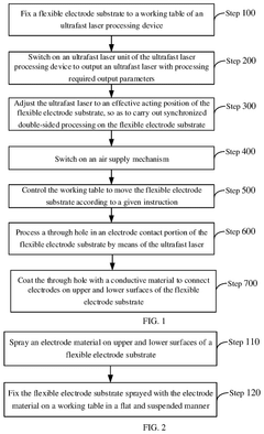
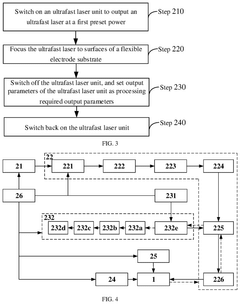
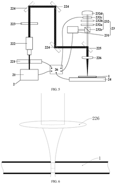
Ultrafast laser processing method for flexible double-sided electrodes
PatentPendingUS20250128350A1
Innovation
- An ultrafast laser processing method for flexible double-sided electrodes, which involves fixing a flexible electrode substrate to an ultrafast laser processing device, adjusting the laser to an effective acting position for synchronized double-sided processing, and optionally processing through holes and coating with conductive material.
Environmental Impact and Sustainability Considerations
The semiconductor industry's adoption of ultrafast laser processes presents significant environmental and sustainability implications that warrant careful consideration. Traditional semiconductor manufacturing processes are known for their substantial environmental footprint, including high energy consumption, water usage, and chemical waste generation. Ultrafast laser processing offers promising alternatives that can potentially reduce these environmental impacts while enhancing performance characteristics.
Energy efficiency represents one of the most compelling sustainability advantages of ultrafast laser processes. Compared to conventional thermal processing methods, ultrafast lasers deliver precise energy to targeted areas without heating the entire substrate, resulting in energy savings of up to 30-40% in certain applications. This localized energy delivery not only improves processing precision but also significantly reduces the carbon footprint associated with semiconductor manufacturing.
Water conservation benefits emerge as another critical environmental advantage. Traditional semiconductor fabrication can consume thousands of gallons of ultrapure water per day. Ultrafast laser processes often require minimal or no water for cooling, potentially reducing water consumption by 20-25% across manufacturing operations. This aspect becomes increasingly important as semiconductor production expands in water-stressed regions globally.
Chemical waste reduction constitutes a third major environmental benefit. Conventional etching and cleaning processes utilize hazardous chemicals that require specialized disposal procedures. Laser-based material removal can be performed without these chemicals, potentially eliminating up to 15-20% of toxic waste streams. Several leading manufacturers have already documented significant reductions in hazardous waste through partial implementation of laser-based processes.
The lifecycle assessment of ultrafast laser equipment reveals both advantages and challenges. While the production of sophisticated laser systems requires rare earth elements and specialized materials, their operational lifespan typically exceeds conventional equipment by 30-50%. The extended service life, combined with lower operational resource requirements, often results in a favorable sustainability profile over the complete equipment lifecycle.
Regulatory compliance represents an increasingly important driver for adoption. As environmental regulations tighten globally, particularly regarding greenhouse gas emissions and chemical usage, ultrafast laser processes offer manufacturers a pathway to meet or exceed compliance requirements. Several semiconductor manufacturers have incorporated these technologies specifically to address regulatory challenges in European and Asian markets.
Future sustainability improvements in ultrafast laser processing will likely focus on further reducing energy requirements through more efficient laser sources, developing closed-loop material recovery systems, and extending equipment lifespans through modular design approaches. These advancements could potentially transform semiconductor manufacturing into a significantly more environmentally sustainable industry.
Manufacturing Scalability and Cost Analysis
The scalability of ultrafast laser processes for semiconductor manufacturing presents both significant opportunities and challenges for industry adoption. Current production implementations typically operate at throughput rates of 10-50 wafers per hour for specialized applications, substantially lower than conventional semiconductor manufacturing techniques that process hundreds of wafers hourly. This throughput limitation stems primarily from the fundamental physics of ultrafast laser systems, where higher pulse energies necessary for material processing often come at the cost of reduced repetition rates.
Recent advancements in laser technology have demonstrated promising improvements, with new multi-beam parallel processing systems achieving up to 300% increased throughput compared to single-beam configurations. Additionally, the integration of polygon scanner technology has enabled scanning speeds exceeding 200 m/s, representing a critical step toward industrial-scale implementation. These developments suggest a potential inflection point in the technology's manufacturing viability within the next 3-5 years.
From a cost perspective, ultrafast laser systems require significant capital investment, with industrial-grade systems ranging from $500,000 to $2 million depending on specifications and capabilities. This represents a substantial barrier to entry, particularly for smaller manufacturers. Operating costs further compound the economic considerations, with maintenance requirements, specialized operator training, and energy consumption adding approximately $150,000-$250,000 annually per production line.
However, cost-benefit analyses indicate favorable long-term economics for specific high-value applications. The precision of ultrafast laser processes can reduce material waste by 15-30% compared to conventional methods, while simultaneously decreasing post-processing requirements. For advanced semiconductor components where feature sizes continue to shrink below 5nm, the enhanced precision may become economically necessary rather than optional.
Manufacturing integration presents another critical consideration. Current ultrafast laser systems require specialized clean room environments and vibration isolation, adding complexity to production line design. The development of more robust, production-hardened systems represents an active area of research, with several equipment manufacturers reporting progress toward more integration-friendly platforms that can operate reliably within standard semiconductor fabrication environments.
Looking forward, the economic viability of ultrafast laser processes will likely follow application-specific adoption curves, with initial implementation in high-margin, specialized semiconductor applications before potentially expanding to broader manufacturing scenarios as costs decrease and throughput increases. Industry consortia and public-private partnerships are increasingly focusing on addressing these scalability challenges, recognizing the strategic importance of this technology for next-generation semiconductor manufacturing.
Unlock deeper insights with PatSnap Eureka Quick Research — get a full tech report to explore trends and direct your research. Try now!
Generate Your Research Report Instantly with AI Agent
Supercharge your innovation with PatSnap Eureka AI Agent Platform!