

Evaluating Polysilane's Application in Smart Home Technology?
JUL 11, 20259 MIN READ
Generate Your Research Report Instantly with AI Agent
PatSnap Eureka helps you evaluate technical feasibility & market potential.
Polysilane Background and Smart Home Goals
Polysilane, a class of silicon-based polymers, has emerged as a promising material in the field of smart home technology. The evolution of polysilane research can be traced back to the 1920s when initial studies on organosilicon compounds began. However, it wasn't until the 1980s that significant breakthroughs in polysilane synthesis and characterization were achieved, paving the way for their potential applications in various fields, including electronics and optoelectronics.
The unique electronic and optical properties of polysilanes, stemming from their σ-conjugated backbone, have attracted considerable attention in recent years. These properties include high photosensitivity, excellent charge carrier mobility, and tunable bandgap, making polysilanes particularly suitable for integration into smart home technologies. As the smart home market continues to grow rapidly, there is an increasing demand for advanced materials that can enhance the performance and functionality of various devices and systems.
In the context of smart home technology, the primary goal of polysilane application is to leverage its unique properties to develop more efficient, responsive, and versatile devices. One key objective is to improve the performance of sensors and detectors used in smart home systems. Polysilanes' high photosensitivity and fast response to light make them ideal candidates for developing advanced optical sensors, which can be utilized in various applications such as ambient light detection, occupancy sensing, and even gesture recognition.
Another important goal is to enhance the energy efficiency of smart home devices. Polysilanes' excellent charge carrier mobility can be exploited to develop more efficient organic light-emitting diodes (OLEDs) and organic photovoltaic cells (OPVs). These improvements could lead to energy-saving lighting solutions and more effective solar energy harvesting systems for smart homes.
Furthermore, the integration of polysilanes into smart home technology aims to enable the development of flexible and wearable electronics. The ability to process polysilanes into thin films and their compatibility with various substrates make them suitable for creating bendable displays, touch-sensitive surfaces, and wearable sensors that can seamlessly integrate into the smart home ecosystem.
As research in polysilane technology progresses, the overarching goal is to create a new generation of smart home devices that are not only more efficient and responsive but also more sustainable and environmentally friendly. By harnessing the unique properties of polysilanes, researchers and developers aspire to push the boundaries of what is possible in smart home technology, ultimately enhancing the quality of life for users while minimizing environmental impact.
Smart Home Market Demand Analysis
The smart home market has experienced significant growth in recent years, driven by increasing consumer demand for convenience, energy efficiency, and enhanced home security. As of 2023, the global smart home market is valued at approximately $112 billion, with projections indicating a compound annual growth rate (CAGR) of 25.3% from 2023 to 2030. This rapid expansion is fueled by advancements in Internet of Things (IoT) technology, artificial intelligence, and the proliferation of connected devices.
Consumer adoption of smart home technologies has been steadily increasing, with smart speakers and smart lighting systems leading the way as entry points for many households. The COVID-19 pandemic has further accelerated this trend, as people spent more time at home and sought ways to improve their living spaces. This has led to a surge in demand for smart home devices that enhance comfort, productivity, and entertainment.
Energy management and sustainability have emerged as key drivers in the smart home market. Consumers are increasingly looking for solutions that can help reduce their energy consumption and carbon footprint. Smart thermostats, energy monitoring systems, and automated lighting controls are among the most sought-after products in this category. The integration of renewable energy sources, such as solar panels, with smart home systems is also gaining traction.
Home security and surveillance systems represent another significant segment of the smart home market. The demand for connected cameras, smart doorbells, and intelligent locks has been growing steadily, driven by consumers' desire for enhanced safety and peace of mind. The ability to remotely monitor and control these devices through smartphones has been a key selling point.
The healthcare sector is emerging as a promising area for smart home technology applications. With an aging population in many developed countries, there is increasing demand for home-based healthcare solutions. Smart home devices that can monitor vital signs, detect falls, and assist with medication management are gaining popularity among elderly consumers and their caregivers.
Interoperability and seamless integration between different smart home devices and platforms remain a challenge in the market. Consumers are seeking solutions that can work together harmoniously, regardless of the manufacturer. This has led to the development of industry standards and protocols aimed at improving device compatibility and user experience.
As the smart home market continues to evolve, there is growing interest in more advanced and specialized applications. This includes the potential use of novel materials and technologies, such as polysilane, to enhance the functionality and performance of smart home devices. The market demand for innovative solutions that can offer unique benefits in terms of energy efficiency, durability, or sensing capabilities presents opportunities for new materials to make their mark in the smart home ecosystem.
Polysilane Technology Status and Challenges
Polysilane technology, while promising in various applications, faces several challenges in its current state of development for smart home technology. The synthesis and processing of polysilanes remain complex and costly, limiting their widespread adoption in consumer electronics. Current manufacturing methods often involve harsh conditions and toxic precursors, posing environmental and safety concerns that need to be addressed for large-scale production.
One of the primary technical hurdles is the stability of polysilanes under ambient conditions. Many polysilane compounds are sensitive to light and oxygen, which can lead to degradation and loss of their unique electronic properties. This instability presents a significant obstacle for their integration into smart home devices that require long-term reliability and consistent performance.
The electrical conductivity of polysilanes, while notable for organic materials, still falls short of traditional inorganic semiconductors used in electronic devices. Enhancing the conductivity and charge carrier mobility of polysilanes remains a key focus area for researchers aiming to improve their viability in smart home applications.
Another challenge lies in the integration of polysilanes with existing smart home technologies. Compatibility issues with current manufacturing processes and materials used in consumer electronics need to be resolved to facilitate seamless incorporation of polysilane-based components into smart home devices.
The development of efficient and cost-effective methods for patterning and depositing polysilanes on various substrates is crucial for their application in smart home technology. Current techniques often lack the precision and scalability required for mass production of consumer electronics.
Globally, research on polysilanes is concentrated in a few countries, with Japan, the United States, and Germany leading in patent filings and academic publications. This geographical concentration of expertise may limit the rapid dissemination and advancement of polysilane technology worldwide.
Despite these challenges, recent advancements in polysilane chemistry have shown promise. Researchers have made progress in developing more stable polysilane derivatives and improving their processability. Novel synthesis routes using milder conditions and more environmentally friendly precursors are being explored, addressing some of the production-related concerns.
The potential of polysilanes in smart home technology lies in their unique optoelectronic properties and their ability to be tailored for specific applications. As research continues to overcome current limitations, polysilanes could enable the development of more efficient, flexible, and multifunctional smart home devices, potentially revolutionizing areas such as displays, sensors, and energy management systems.
Current Polysilane Applications in Smart Homes
01 Synthesis and properties of polysilanes
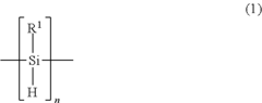
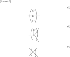
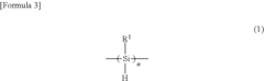
Polysilanes are synthesized through various methods and exhibit unique properties. These silicon-based polymers have applications in electronics, optics, and materials science due to their electronic and optical characteristics. The synthesis methods and resulting properties can be tailored for specific applications.- Synthesis and properties of polysilanes: Polysilanes are silicon-based polymers with unique electronic and optical properties. They can be synthesized through various methods, including Wurtz coupling of dichlorosilanes. These polymers exhibit interesting characteristics such as photoconductivity, luminescence, and high thermal stability, making them suitable for various applications in electronics and materials science.
- Applications of polysilanes in photoresists and lithography: Polysilanes have found significant use in photoresist formulations and lithographic processes. Their photosensitivity and ability to undergo photochemical reactions make them valuable in the production of microelectronic devices and semiconductor manufacturing. They can be used as positive or negative photoresists, offering high resolution and good etching resistance.
- Polysilane-based coatings and films: Polysilanes can be used to create thin films and coatings with unique properties. These films can exhibit excellent adhesion to various substrates, high thermal stability, and good optical transparency. They find applications in protective coatings, optical coatings, and as precursors for ceramic materials.
- Functionalization and modification of polysilanes: Polysilanes can be functionalized or modified to enhance their properties or introduce new functionalities. This can involve the incorporation of various organic groups, metal atoms, or other elements into the polymer backbone or as side chains. Such modifications can lead to improved solubility, processability, or specific functional properties tailored for particular applications.
- Polysilanes as precursors for silicon-based materials: Polysilanes serve as valuable precursors for the production of various silicon-based materials. Through controlled thermal decomposition or other conversion processes, they can be transformed into silicon carbide, silicon nitride, or other ceramic materials. This approach allows for the fabrication of advanced materials with tailored properties for applications in high-temperature environments or electronic devices.
02 Polysilane-based coatings and films
Polysilanes are used to create coatings and films with specific properties. These coatings can be applied to various substrates and may offer benefits such as improved durability, optical properties, or electronic characteristics. The formulation and application methods of polysilane-based coatings are crucial for their performance.Expand Specific Solutions03 Polysilanes in photoresist applications
Polysilanes are utilized in photoresist formulations for semiconductor manufacturing. Their unique properties make them suitable for lithography processes, allowing for the creation of fine patterns on substrates. The development of polysilane-based photoresists involves optimizing their photosensitivity and resolution capabilities.Expand Specific Solutions04 Functionalization and modification of polysilanes
Polysilanes can be functionalized or modified to enhance their properties or introduce new functionalities. This includes the addition of various side groups or the incorporation of other elements into the polymer backbone. These modifications allow for the tailoring of polysilanes for specific applications or to improve their compatibility with other materials.Expand Specific Solutions05 Polysilanes in electronic and optical devices
Polysilanes are employed in the development of electronic and optical devices. Their unique electronic structure and optical properties make them suitable for applications such as light-emitting diodes, photovoltaic cells, and other optoelectronic devices. The processing and integration of polysilanes into these devices are areas of ongoing research and development.Expand Specific Solutions
Key Players in Polysilane and Smart Home Industries
The application of polysilane in smart home technology is in an early developmental stage, with the market still emerging and relatively small. The technology's maturity is low, indicating significant room for innovation and growth. Key players in this field include Wacker Chemie AG, a leading chemical company with expertise in silicone-based products, and Air Liquide SA, which has a strong presence in industrial gases and advanced materials. Japanese firms like Osaka Gas Co., Ltd. and Toagosei Co., Ltd. are also exploring polysilane applications, leveraging their chemical industry experience. Research institutions such as Japan Science & Technology Agency and Kanazawa University are contributing to the fundamental understanding of polysilane properties, potentially accelerating its adoption in smart home technologies.
Wacker Chemie AG
Technical Solution: Wacker Chemie AG has developed innovative polysilane-based materials for smart home applications. Their approach involves synthesizing high-purity polysilanes with tailored molecular structures to enhance electrical and optical properties. These materials are used in the production of thin-film transistors for flexible displays and touch sensors in smart home devices[1]. Wacker's polysilanes also demonstrate excellent photosensitivity, making them suitable for light-sensitive switches and sensors in automated lighting systems[2]. The company has further explored the integration of polysilanes into self-cleaning coatings for smart windows, leveraging the material's unique surface properties[3].
Strengths: High-purity synthesis, customizable properties, versatile applications in displays and sensors. Weaknesses: Potentially higher production costs, limited long-term stability data in real-world smart home environments.
Japan Science & Technology Agency
Technical Solution: The Japan Science & Technology Agency has conducted extensive research on polysilane applications in smart home technology. Their approach focuses on developing polysilane-based organic photovoltaic (OPV) materials for energy-efficient smart windows and building-integrated photovoltaics[4]. By optimizing the molecular structure of polysilanes, researchers have achieved improved light absorption and charge transport properties, resulting in OPV devices with enhanced power conversion efficiencies[5]. Additionally, the agency has explored the use of polysilanes in flexible, large-area sensors for smart home security and environmental monitoring systems, leveraging the material's unique optoelectronic properties[6].
Strengths: Cutting-edge research in energy harvesting and sensing applications, potential for high-efficiency devices. Weaknesses: Technology still in research phase, may require significant time and investment for commercialization.
Key Polysilane Innovations for Smart Home Use
Polysilane and polysilane-containing resin composition
PatentInactiveUS8163863B2
Innovation
- Introducing a Si—H group into the polysilane main chain and bonding a hydrosilylatable compound with functional groups like hydroxyl, carboxyl, or epoxy groups, allowing for controlled hydrosilylation to enhance solubility and reactivity without complex steps or special apparatus.

Photoluminescent and/or electroluminescent material, method for production and use thereof and component comprising such a material
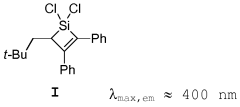
PatentWO2013068490A1
Innovation
- Development of polysilanes with stilbene and styrene units that are crosslinked to form stable, moisture-resistant materials with enhanced luminescence efficiency, suitable for use in optoelectronic components.
Environmental Impact of Polysilane in Smart Homes
The integration of polysilane in smart home technology brings both potential benefits and environmental concerns. As an emerging material, polysilane's environmental impact in smart homes requires careful consideration across its entire lifecycle, from production to disposal.
During the manufacturing process of polysilane-based smart home devices, the production of polysilane itself may involve energy-intensive processes and the use of potentially hazardous chemicals. This could contribute to increased carbon emissions and chemical waste if not properly managed. However, advancements in green chemistry and sustainable manufacturing practices may help mitigate these impacts over time.
In the usage phase, polysilane-based smart home technologies could potentially lead to energy savings through improved efficiency in lighting, heating, and cooling systems. The material's unique properties, such as its high electron mobility and sensitivity to environmental changes, may enable more precise control and optimization of home energy consumption. This could result in a net positive environmental impact by reducing overall household energy usage and associated carbon emissions.
The durability and longevity of polysilane-based devices are crucial factors in assessing their environmental footprint. If these devices prove to be more resilient and longer-lasting than traditional alternatives, it could reduce electronic waste generation. However, if the technology leads to rapid obsolescence and frequent replacements, it may exacerbate e-waste issues.
End-of-life considerations for polysilane-based smart home devices are particularly important. The recyclability and biodegradability of polysilane components need to be thoroughly investigated. If polysilane can be easily separated and recycled, it could contribute to a more circular economy in the smart home sector. However, if recycling processes are complex or energy-intensive, it may offset some of the material's environmental benefits.
The potential release of nanoparticles or degradation products from polysilane-based devices into the home environment is another area of concern. Long-term studies on the health and environmental impacts of these potential emissions are necessary to ensure the safety of residents and ecosystems.
As smart home technology becomes more prevalent, the cumulative environmental impact of polysilane-based devices across millions of households must be considered. While individual devices may have minimal impact, the scale of adoption could lead to significant aggregate effects on resource consumption, energy use, and waste generation.
In conclusion, the environmental impact of polysilane in smart homes is a complex issue that requires a holistic approach to assessment. While the material shows promise for enhancing energy efficiency and device performance, careful attention must be paid to its production, use, and disposal to ensure that its integration into smart home technology results in a net positive environmental outcome.
Polysilane Manufacturing and Supply Chain Analysis
The manufacturing and supply chain analysis of polysilane for smart home technology applications reveals a complex and evolving landscape. Polysilane production primarily relies on the synthesis of organosilicon compounds, which involves multiple steps and requires specialized equipment. The key raw materials include silicon metal, methyl chloride, and various catalysts, sourced from global suppliers.
The manufacturing process typically begins with the production of methylchlorosilanes through the direct process, followed by the synthesis of polysilanes through dehydrogenative coupling or reductive coupling methods. These processes demand precise control of reaction conditions and often involve energy-intensive steps, impacting the overall cost and environmental footprint of production.
Supply chain considerations for polysilane manufacturing are multifaceted. The primary silicon feedstock is predominantly sourced from China, which controls a significant portion of the global silicon market. This geographical concentration introduces potential supply risks and price volatility. Additionally, the specialized nature of polysilane production equipment limits the number of capable manufacturers, creating potential bottlenecks in scaling up production to meet growing demand in the smart home sector.
Transportation and storage of polysilanes present unique challenges due to their sensitivity to moisture and air. Specialized packaging and handling procedures are necessary to maintain product integrity throughout the supply chain, adding complexity and cost to logistics operations.
The smart home technology industry's increasing interest in polysilane applications has spurred efforts to optimize manufacturing processes and streamline supply chains. Innovations in continuous flow chemistry and process intensification are being explored to enhance production efficiency and reduce costs. Furthermore, efforts to diversify silicon sources and develop alternative synthesis routes are underway to mitigate supply chain risks and improve sustainability.
As the demand for polysilane in smart home applications grows, manufacturers are investing in capacity expansion and vertical integration strategies. This includes establishing partnerships with raw material suppliers and end-users to ensure a stable supply chain and foster collaborative innovation. However, challenges remain in scaling production to meet potential future demand while maintaining product quality and cost-effectiveness.
Unlock deeper insights with PatSnap Eureka Quick Research — get a full tech report to explore trends and direct your research. Try now!
Generate Your Research Report Instantly with AI Agent
Supercharge your innovation with PatSnap Eureka AI Agent Platform!