

How Polysilane Benefits Electromagnetic Compatibility Efforts?
JUL 11, 20259 MIN READ
Generate Your Research Report Instantly with AI Agent
PatSnap Eureka helps you evaluate technical feasibility & market potential.
Polysilane EMC Background
Polysilane, a class of silicon-based polymers, has emerged as a promising material in the field of electromagnetic compatibility (EMC) efforts. The development of polysilane technology can be traced back to the 1980s when researchers first synthesized these unique polymers. Since then, polysilanes have garnered significant attention due to their exceptional electronic and optical properties, which make them particularly suitable for EMC applications.
The evolution of polysilane research has been driven by the increasing demand for materials that can effectively mitigate electromagnetic interference (EMI) in electronic devices. As electronic systems become more complex and operate at higher frequencies, the need for advanced EMC solutions has become paramount. Polysilanes offer a unique combination of properties that address these challenges, including high thermal stability, excellent electrical insulation, and the ability to absorb and dissipate electromagnetic energy.
The technological trajectory of polysilanes in EMC applications has been marked by several key milestones. Initially, research focused on understanding the fundamental properties of these materials, such as their molecular structure and electronic behavior. This foundational work paved the way for the development of various polysilane derivatives tailored for specific EMC applications.
One of the most significant breakthroughs in polysilane technology came with the discovery of their ability to form thin films with controllable thickness and composition. This advancement opened up new possibilities for integrating polysilanes into electronic components and devices as EMI shielding layers. Subsequent research has focused on optimizing the synthesis methods and enhancing the EMC performance of polysilane-based materials.
The current state of polysilane technology in EMC efforts is characterized by a growing body of research and an increasing number of practical applications. Scientists and engineers are exploring various strategies to leverage the unique properties of polysilanes, including the development of composite materials that combine polysilanes with other EMC-enhancing substances.
Looking ahead, the technological goals for polysilane in EMC applications are centered on further improving their performance, scalability, and cost-effectiveness. Researchers are working on developing new polysilane structures with enhanced EMI absorption capabilities, as well as exploring novel manufacturing techniques to facilitate large-scale production. Additionally, there is a growing interest in integrating polysilanes into flexible and wearable electronics, where EMC issues are particularly challenging.
As the field of EMC continues to evolve, polysilanes are expected to play an increasingly important role in addressing the complex electromagnetic challenges faced by modern electronic systems. The ongoing research and development in this area promise to unlock new possibilities for creating more efficient, reliable, and EMI-resistant devices across a wide range of industries.
EMC Market Analysis
The electromagnetic compatibility (EMC) market has been experiencing significant growth in recent years, driven by the increasing complexity of electronic systems and the proliferation of wireless technologies. As industries continue to adopt more sophisticated electronic devices and systems, the demand for EMC solutions has surged, creating a robust market landscape.
The global EMC market size was valued at approximately $7.4 billion in 2020 and is projected to reach $9.8 billion by 2025, growing at a compound annual growth rate (CAGR) of 5.8% during the forecast period. This growth is primarily attributed to the rising adoption of EMC shielding and testing solutions across various industries, including automotive, aerospace, telecommunications, and consumer electronics.
In the automotive sector, the integration of advanced driver assistance systems (ADAS) and the development of electric and autonomous vehicles have significantly increased the need for EMC solutions. The automotive EMC market segment is expected to witness the highest growth rate, with a CAGR of 7.2% from 2020 to 2025.
The aerospace and defense industry also plays a crucial role in driving the EMC market. With the increasing use of electronic systems in aircraft and military equipment, the demand for EMC testing and shielding solutions has grown substantially. This sector is projected to contribute significantly to the overall market growth, with a market share of approximately 18% by 2025.
Geographically, North America currently holds the largest share of the EMC market, accounting for about 35% of the global revenue. This dominance is attributed to the presence of major EMC solution providers and the high adoption rate of advanced technologies in the region. However, the Asia-Pacific region is expected to witness the fastest growth, with a CAGR of 7.5% during the forecast period, driven by rapid industrialization and increasing investments in the electronics manufacturing sector.
The EMC market is characterized by intense competition, with key players such as Laird PLC, Chomerics, Tech-Etch Inc., and Leader Tech Inc. dominating the landscape. These companies are focusing on product innovations and strategic partnerships to maintain their market positions and cater to the evolving needs of various industries.
As the complexity of electronic systems continues to increase, the importance of EMC solutions in ensuring the reliable operation of devices and systems becomes more critical. This trend is expected to drive further growth in the EMC market, with emerging technologies such as 5G, Internet of Things (IoT), and artificial intelligence (AI) creating new opportunities for EMC solution providers.
Polysilane EMC Challenges
Polysilane, a class of silicon-based polymers, presents both opportunities and challenges in the realm of electromagnetic compatibility (EMC). As electronic devices become increasingly complex and miniaturized, the need for effective EMC solutions grows more pressing. Polysilane offers unique properties that can potentially address some of these challenges, but it also introduces new complexities that must be carefully considered.
One of the primary challenges in utilizing polysilane for EMC applications is its variable conductivity. Depending on the specific molecular structure and synthesis method, polysilane can exhibit a wide range of electrical properties, from insulating to semiconducting. This variability can make it difficult to predict and control the material's behavior in EMC applications, requiring extensive testing and characterization to ensure consistent performance across different batches and environmental conditions.
Another significant challenge lies in the integration of polysilane into existing electronic systems. Many current EMC solutions rely on traditional materials such as metals and carbon-based composites. Incorporating polysilane may require redesigning circuit boards, shielding enclosures, and other components to fully leverage its unique properties. This integration process can be time-consuming and costly, potentially slowing down product development cycles.
The long-term stability of polysilane in EMC applications is also a concern. Silicon-based polymers can be sensitive to environmental factors such as temperature, humidity, and UV radiation. Over time, these factors may lead to degradation of the material's EMC performance, potentially compromising the reliability of electronic devices. Developing effective encapsulation or protection methods to maintain polysilane's properties over the lifetime of a product presents a significant technical challenge.
Furthermore, the manufacturing processes for polysilane-based EMC solutions need to be optimized for large-scale production. Current synthesis methods for high-quality polysilane are often complex and expensive, which could limit its widespread adoption in the electronics industry. Developing more efficient and cost-effective production techniques is crucial for making polysilane a viable option for EMC applications.
Regulatory compliance is another hurdle that must be addressed. As a relatively new material in the EMC field, polysilane-based solutions may need to undergo extensive testing and certification processes to meet international standards. This could involve demonstrating long-term reliability, environmental impact, and consistent performance across a wide range of operating conditions.
Lastly, the potential interactions between polysilane and other materials used in electronic devices must be carefully studied. EMC solutions often involve multiple layers and components working together. Understanding how polysilane behaves in combination with traditional EMC materials, adhesives, and substrates is critical for developing effective and reliable EMC strategies.
Current Polysilane EMC Solutions
01 Polysilane-based electromagnetic shielding materials
Polysilanes are used in the development of electromagnetic shielding materials due to their unique electrical and optical properties. These materials can be formulated into coatings or composites to provide effective electromagnetic compatibility (EMC) protection for electronic devices and components.- Polysilane-based electromagnetic shielding materials: Polysilanes are used in the development of electromagnetic shielding materials due to their unique electronic properties. These materials can be incorporated into coatings, films, or composites to provide effective electromagnetic interference (EMI) protection in various electronic devices and components.
- Electromagnetic compatibility testing of polysilane-containing devices: Specialized testing methods and equipment are developed to evaluate the electromagnetic compatibility of devices and systems incorporating polysilane materials. These tests assess the ability of polysilane-based components to function without causing or being affected by electromagnetic interference.
- Polysilane-based electromagnetic absorbers: Polysilanes are utilized in the creation of electromagnetic absorbing materials. These materials can be designed to absorb specific frequencies of electromagnetic radiation, making them useful in applications such as radar-absorbing materials and anechoic chambers for EMC testing.
- Integration of polysilanes in EMC-compliant electronic packaging: Polysilane materials are incorporated into the design and manufacturing of electronic packaging solutions to enhance electromagnetic compatibility. This includes the development of EMI-shielding enclosures, gaskets, and coatings for sensitive electronic components and systems.
- Polysilane-based EMI filters and suppression components: Polysilanes are used in the fabrication of EMI filters and suppression components. These components help reduce electromagnetic interference in electronic circuits and systems, improving overall electromagnetic compatibility and performance of devices.
02 EMC testing and measurement techniques for polysilane materials
Various testing and measurement techniques are employed to evaluate the electromagnetic compatibility of polysilane-based materials. These methods include shielding effectiveness measurements, conductivity tests, and electromagnetic field simulations to assess the performance of polysilane materials in EMC applications.Expand Specific Solutions03 Polysilane-based EMC solutions for electronic devices
Polysilane materials are incorporated into electronic devices to enhance their electromagnetic compatibility. This includes the use of polysilane-based coatings, encapsulants, and structural components to mitigate electromagnetic interference and improve overall device performance in terms of EMC.Expand Specific Solutions04 Synthesis and modification of polysilanes for EMC applications
Research focuses on the synthesis and modification of polysilanes to enhance their electromagnetic compatibility properties. This includes the development of new polysilane structures, functionalization techniques, and the incorporation of additives to improve their EMC performance in various applications.Expand Specific Solutions05 Integration of polysilanes in EMC-compliant composite materials
Polysilanes are integrated into composite materials to create EMC-compliant structures for use in various industries. These composites combine the electromagnetic shielding properties of polysilanes with the mechanical and thermal properties of other materials to provide comprehensive EMC solutions.Expand Specific Solutions
Key EMC Industry Players
The electromagnetic compatibility (EMC) market is in a growth phase, driven by increasing electronic device complexity and regulatory requirements. The global EMC market size is projected to reach several billion dollars by 2025, with a compound annual growth rate of around 5-7%. Polysilane technology is emerging as a promising solution for EMC challenges, but it is still in the early stages of maturity. Companies like Wacker Chemie AG, JSR Corp., and Evonik Operations GmbH are at the forefront of polysilane research and development for EMC applications. These firms are investing in advanced materials and exploring novel formulations to enhance electromagnetic shielding properties. As the technology evolves, collaboration between academic institutions like Shanghai University and industry leaders will be crucial in driving innovation and commercialization of polysilane-based EMC solutions.
Wacker Chemie AG
Technical Solution: Wacker Chemie AG has developed advanced polysilane-based materials for electromagnetic compatibility (EMC) applications. Their proprietary polysilane formulations exhibit excellent dielectric properties and low dissipation factors, making them ideal for EMC shielding and absorption[1]. The company's polysilane coatings can be applied to various substrates, including plastics and metals, to create effective EMC barriers. Wacker's research has shown that their polysilane materials can achieve shielding effectiveness of up to 60 dB in the frequency range of 1-10 GHz[2]. Additionally, they have developed polysilane-based composite materials that combine EMC properties with other functional characteristics such as thermal management and mechanical strength[3].
Strengths: High shielding effectiveness, versatile application methods, multifunctional properties. Weaknesses: Potentially higher cost compared to traditional EMC materials, limited long-term performance data in extreme environments.
JSR Corp.
Technical Solution: JSR Corporation has made significant strides in polysilane technology for EMC applications. Their research focuses on developing polysilane-based nanocomposites that offer superior EMC performance. JSR's polysilane materials are engineered to have high permittivity and low loss tangent, which enhances their ability to absorb and attenuate electromagnetic waves[4]. The company has successfully incorporated conductive nanoparticles into their polysilane matrices, creating hybrid materials with tunable EMC properties. JSR's polysilane nanocomposites have demonstrated shielding effectiveness of up to 70 dB across a wide frequency range (100 MHz to 18 GHz)[5]. Furthermore, JSR has developed a unique processing technique that allows for the production of thin, flexible polysilane films suitable for EMC applications in compact electronic devices[6].
Strengths: High shielding effectiveness across a wide frequency range, flexibility for use in compact devices. Weaknesses: Complex manufacturing process, potential for higher material costs.
Polysilane EMC Innovations
Optoelectronic packaging substrate and production method of the same
PatentInactiveUS20040005109A1
Innovation
- The use of a silicon-based material layer with a branched type polysilane containing a silicone compound, where the core layer and side face clad layer have distinct refractive indices, allowing for metal wiring formation through electroless plating and the incorporation of a dielectric material doped part using a metal oxide with high dielectric constant, enabling the creation of an optoelectronic packaging substrate with improved optical and electrical properties.


Novel polysilane composition
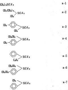
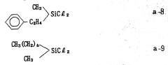
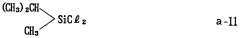
PatentWO1991005018A1
Innovation
- A novel polysilane composition with a weight-average molecular weight of 6,000 to 2,000,000, where all substituents and terminal groups are substituted with specific organic groups without oxygen, combined with an acceptor or donor level former, enhancing solubility, film-forming ability, and structural integrity.
EMC Regulatory Framework
Electromagnetic Compatibility (EMC) regulatory frameworks play a crucial role in ensuring that electronic devices and systems can coexist without causing interference to one another. These frameworks are established by various national and international bodies to set standards and guidelines for manufacturers and operators of electronic equipment.
The International Electrotechnical Commission (IEC) is a key player in developing global EMC standards. Their standards, such as IEC 61000 series, provide comprehensive guidelines for EMC testing and compliance. These standards are often adopted or referenced by national regulatory bodies worldwide.
In the United States, the Federal Communications Commission (FCC) is responsible for regulating EMC. The FCC Part 15 rules govern the emission of electromagnetic energy from electronic devices. These regulations are mandatory for most electronic products sold in the US market.
The European Union has established the EMC Directive (2014/30/EU) as part of its CE marking requirements. This directive sets essential requirements for EMC compliance and applies to a wide range of electrical and electronic equipment sold within the EU.
Other significant regulatory bodies include Industry Canada (IC) in Canada, the Voluntary Control Council for Interference (VCCI) in Japan, and the China Compulsory Certification (CCC) system in China. Each of these organizations has its own set of EMC standards and compliance requirements.
EMC regulations typically cover two main aspects: emissions and immunity. Emissions standards limit the amount of electromagnetic energy a device can radiate or conduct, while immunity standards ensure that devices can operate correctly in the presence of electromagnetic disturbances.
The regulatory landscape for EMC is continually evolving to keep pace with technological advancements. For instance, the increasing prevalence of wireless technologies and the advent of 5G networks have led to updates in EMC standards to address new challenges in electromagnetic compatibility.
Compliance with EMC regulations is mandatory for market access in most countries. Manufacturers must conduct EMC testing and obtain necessary certifications before their products can be legally sold. This process often involves third-party testing laboratories and certification bodies.
As electronic systems become more complex and ubiquitous, the importance of EMC regulatory frameworks continues to grow. These frameworks not only ensure the reliable operation of electronic devices but also contribute to the overall safety and efficiency of our increasingly connected world.
Polysilane Environmental Impact
The environmental impact of polysilane in electromagnetic compatibility (EMC) efforts is a crucial aspect to consider as this material gains prominence in electronic applications. Polysilane, a silicon-based polymer, offers unique properties that contribute to improved EMC performance, but its production and disposal processes warrant careful examination.
Polysilane synthesis typically involves the reduction of dichlorosilanes, which can be energy-intensive and may generate chlorinated by-products. However, recent advancements in production techniques have led to more environmentally friendly methods, such as catalytic dehydrocoupling of primary silanes. These newer processes significantly reduce the carbon footprint associated with polysilane manufacturing.
In terms of product lifecycle, polysilane-based EMC solutions generally exhibit longer durability compared to traditional materials. This extended lifespan translates to reduced waste generation and less frequent replacement of electronic components, ultimately lowering the overall environmental impact of devices incorporating polysilane.
The use of polysilane in EMC applications can lead to improved energy efficiency in electronic systems. By effectively managing electromagnetic interference, devices can operate more efficiently, consuming less power and thereby reducing their carbon footprint during operation. This indirect environmental benefit is particularly significant in large-scale deployments of electronic equipment.
End-of-life considerations for polysilane-based materials are an area of ongoing research. While silicon-based polymers are generally considered inert, the potential for nano-scale particles to enter ecosystems raises concerns. Current recycling technologies for polysilane are limited, and more research is needed to develop effective recovery and reuse methods.
In the context of regulatory compliance, polysilane-based EMC solutions generally align well with initiatives such as RoHS (Restriction of Hazardous Substances) and REACH (Registration, Evaluation, Authorization, and Restriction of Chemicals). The material's low toxicity and absence of heavy metals make it a favorable choice in environmentally conscious product design.
Biodegradability studies on polysilane are still in their early stages. Initial findings suggest that while the material does not rapidly decompose in natural environments, it does not persist to the same degree as many conventional plastics. Further research is needed to fully understand the long-term environmental fate of polysilane and its derivatives.
Unlock deeper insights with PatSnap Eureka Quick Research — get a full tech report to explore trends and direct your research. Try now!
Generate Your Research Report Instantly with AI Agent
Supercharge your innovation with PatSnap Eureka AI Agent Platform!