

How Polysilane Drives Exceptional Device Design Solutions?
JUL 11, 202510 MIN READ
Generate Your Research Report Instantly with AI Agent
PatSnap Eureka helps you evaluate technical feasibility & market potential.
Polysilane Technology Evolution and Objectives
Polysilanes have emerged as a groundbreaking class of materials in the field of device design, offering exceptional properties that drive innovative solutions across various applications. The evolution of polysilane technology can be traced back to the 1980s when researchers first synthesized these silicon-based polymers. Since then, the field has witnessed significant advancements in synthesis methods, characterization techniques, and application development.
The primary objective of polysilane research has been to harness the unique electronic and optical properties of these materials for advanced device applications. Polysilanes exhibit a σ-conjugated backbone structure, which imparts them with remarkable electronic conductivity and photosensitivity. This characteristic has made them particularly attractive for use in optoelectronic devices, photoresists, and photoconductors.
Over the years, researchers have focused on tailoring the molecular structure of polysilanes to enhance their performance in specific applications. This has led to the development of various types of polysilanes, including linear, branched, and cyclic structures, each offering distinct advantages in device design. The ability to fine-tune the properties of polysilanes through molecular engineering has opened up new possibilities in areas such as organic electronics, photovoltaics, and sensors.
One of the key milestones in polysilane technology evolution has been the improvement in their processability and stability. Early polysilanes suffered from poor solubility and susceptibility to oxidation, limiting their practical applications. However, advancements in synthesis techniques and the introduction of protective side groups have significantly enhanced their stability and ease of processing, making them more suitable for large-scale device fabrication.
The integration of polysilanes with other materials has been another important aspect of their technological evolution. Researchers have explored hybrid systems combining polysilanes with inorganic semiconductors, organic polymers, and nanostructures, leading to novel composite materials with enhanced functionalities. These hybrid materials have shown promise in applications ranging from flexible electronics to advanced sensing platforms.
Recent years have seen a growing interest in the use of polysilanes in next-generation device designs. Their unique combination of optical and electronic properties makes them ideal candidates for emerging technologies such as organic light-emitting diodes (OLEDs), thin-film transistors, and photovoltaic cells. The ongoing research aims to further optimize polysilane structures and properties to meet the demanding requirements of these cutting-edge applications.
Looking ahead, the objectives of polysilane technology are focused on addressing key challenges and expanding their potential applications. These include improving the long-term stability of polysilane-based devices, enhancing their charge transport properties, and developing more efficient and scalable synthesis methods. Additionally, there is a growing emphasis on exploring the potential of polysilanes in emerging fields such as quantum computing and bioelectronics, where their unique properties could enable breakthrough innovations.
Market Demand for Polysilane-Based Devices
The market demand for polysilane-based devices has been steadily growing in recent years, driven by the unique properties and versatile applications of polysilanes in various industries. Polysilanes, a class of silicon-based polymers, have garnered significant attention due to their exceptional electronic and optical properties, making them highly desirable for advanced device design solutions.
In the electronics sector, polysilanes have shown great potential in the development of next-generation semiconductors and optoelectronic devices. The increasing demand for high-performance, energy-efficient electronic components has created a substantial market opportunity for polysilane-based materials. These materials offer improved charge carrier mobility and enhanced light-emitting properties, making them ideal for applications in organic light-emitting diodes (OLEDs), photovoltaic cells, and field-effect transistors.
The photonics industry has also recognized the value of polysilanes in developing advanced optical devices. The unique optical properties of polysilanes, including their high refractive indices and tunable bandgaps, have led to their incorporation in waveguides, optical switches, and nonlinear optical materials. As the demand for faster and more efficient optical communication systems continues to rise, the market for polysilane-based photonic devices is expected to expand significantly.
In the field of sensors and detectors, polysilanes have demonstrated remarkable sensitivity and selectivity, particularly in chemical and biological sensing applications. The ability of polysilanes to undergo conformational changes in response to specific stimuli has opened up new possibilities for the development of highly sensitive and selective sensor devices. This has led to increased demand in industries such as healthcare, environmental monitoring, and industrial process control.
The aerospace and defense sectors have also shown growing interest in polysilane-based materials for their potential in developing lightweight, high-strength composites and advanced coatings. The unique combination of thermal stability, radiation resistance, and mechanical properties offered by polysilanes makes them attractive for use in extreme environments and specialized applications.
As the global push for sustainable and environmentally friendly technologies intensifies, the demand for polysilane-based materials in green technologies has surged. Their potential applications in energy storage devices, such as high-capacity batteries and supercapacitors, as well as in advanced water purification systems, have positioned polysilanes as key materials in addressing pressing environmental challenges.
The market demand for polysilane-based devices is further bolstered by ongoing research and development efforts aimed at expanding their applications and improving their performance. As new synthesis methods and processing techniques emerge, the cost-effectiveness and scalability of polysilane production are expected to improve, further driving market growth and adoption across various industries.
Current Polysilane Synthesis Challenges
Polysilane synthesis faces several significant challenges that hinder its widespread adoption in device design solutions. One of the primary obstacles is the difficulty in controlling the molecular weight and polydispersity of polysilanes during synthesis. The Wurtz coupling reaction, a common method for polysilane synthesis, often results in broad molecular weight distributions, which can negatively impact the material's electronic and optical properties.
Another major challenge is the limited solubility of high molecular weight polysilanes in common organic solvents. This solubility issue complicates processing and integration into device fabrication, particularly for applications requiring solution-based deposition techniques. Researchers are actively exploring new synthetic routes and modifications to improve polysilane solubility without compromising its unique properties.
The stability of polysilanes under ambient conditions poses another significant hurdle. Many polysilanes are susceptible to oxidation and photodegradation, which can lead to changes in their electronic structure and overall performance over time. This instability limits the long-term reliability of polysilane-based devices and necessitates the development of more robust synthetic strategies or protective measures.
Scalability and cost-effectiveness of polysilane synthesis remain critical challenges for industrial applications. Current synthetic methods often involve expensive catalysts, stringent reaction conditions, or complex purification processes, making large-scale production economically unfeasible for many potential applications.
Furthermore, the precise control of polysilane backbone structure and side-chain functionalization is crucial for tailoring their properties to specific device requirements. However, achieving this level of structural control while maintaining high yields and purity is technically demanding and often requires sophisticated synthetic approaches.
The environmental impact of polysilane synthesis is also a growing concern. Many traditional synthetic routes involve the use of toxic reagents or generate hazardous byproducts. Developing greener, more sustainable synthesis methods is essential for the long-term viability of polysilane-based technologies.
Lastly, the characterization of polysilanes presents unique challenges due to their sensitivity to light and air. Advanced analytical techniques and specialized handling procedures are often required to accurately determine their structure and properties, which can be time-consuming and resource-intensive.
Addressing these synthesis challenges is crucial for unlocking the full potential of polysilanes in exceptional device design solutions. Ongoing research efforts are focused on developing novel synthetic strategies, improving material stability, and enhancing processing techniques to overcome these obstacles and pave the way for innovative polysilane-based devices.
Existing Polysilane Device Design Solutions
01 Polysilane synthesis and composition
Various methods and compositions for synthesizing polysilanes are described. These include techniques for creating specific molecular structures, controlling molecular weight, and incorporating different functional groups. The resulting polysilanes can have unique properties suitable for device applications.- Polysilane synthesis and composition: Various methods and compositions for synthesizing polysilanes are described. These include techniques for creating specific polysilane structures, controlling molecular weight, and incorporating different functional groups. The resulting polysilanes can have unique properties suitable for device applications.
- Polysilane-based electronic devices: Polysilanes are utilized in the design and fabrication of electronic devices. These materials can be used as active layers in transistors, photovoltaic cells, and other semiconductor devices. The unique electronic properties of polysilanes, such as their conductivity and charge transport characteristics, are exploited in these applications.
- Optical applications of polysilanes: Polysilanes exhibit interesting optical properties that can be harnessed in various devices. These materials can be used in the design of optical waveguides, photoresists, and nonlinear optical devices. The ability to tune the optical properties through structural modifications makes polysilanes versatile for such applications.
- Polysilane thin film deposition techniques: Various methods for depositing polysilane thin films are explored for device fabrication. These include spin-coating, vapor deposition, and plasma-enhanced chemical vapor deposition. The control of film thickness, uniformity, and morphology is crucial for optimal device performance.
- Polysilane-based composite materials: Polysilanes are incorporated into composite materials to enhance their properties for device applications. These composites can combine the unique characteristics of polysilanes with other materials, resulting in improved mechanical, thermal, or electrical properties. Such composites find use in various device designs, including sensors and actuators.
02 Polysilane-based thin films and coatings
Techniques for depositing polysilane thin films and coatings are outlined. These methods include spin-coating, vapor deposition, and other specialized processes. The resulting films can be used in various electronic and optical devices, offering unique properties such as conductivity and photosensitivity.Expand Specific Solutions03 Polysilane applications in electronic devices
Polysilanes are utilized in various electronic device designs, including transistors, photovoltaic cells, and sensors. The unique electronic properties of polysilanes, such as their semiconducting behavior and charge transport capabilities, make them suitable for these applications.Expand Specific Solutions04 Optical and photonic applications of polysilanes
Polysilanes are employed in optical and photonic device designs due to their unique light-responsive properties. Applications include photoresists, optical waveguides, and nonlinear optical materials. The ability to tune the optical properties through molecular design is a key advantage.Expand Specific Solutions05 Polysilane-based composite materials
Composite materials incorporating polysilanes are developed for various device applications. These composites combine the properties of polysilanes with other materials to achieve enhanced performance in areas such as mechanical strength, thermal stability, and electrical conductivity.Expand Specific Solutions
Key Players in Polysilane Research
The polysilane technology market is in a growth phase, driven by increasing demand for advanced device design solutions. The market size is expanding rapidly, with significant potential in electronics, optoelectronics, and semiconductor industries. Technological maturity varies among key players, with companies like JSR Corp., Toray Industries, and Kaneka Corp. leading in research and development. These firms are leveraging their expertise in materials science to advance polysilane applications. Emerging players such as Wanhua Chemical Group and Nagase ChemteX are also making strides, contributing to a competitive landscape. The technology's versatility and performance characteristics are attracting interest from diverse sectors, indicating a promising future for polysilane-based solutions in device design and manufacturing.
Kaneka Corp.
Technical Solution: Kaneka Corporation has developed innovative polysilane-based materials for exceptional device design solutions. Their approach involves synthesizing high-purity polysilanes with controlled molecular weights and structures[1]. These materials exhibit excellent photosensitivity and thermal stability, making them ideal for use in photoresists and electronic devices[2]. Kaneka's polysilanes feature unique silicon-silicon backbones that provide superior electron mobility and light-emitting properties[3]. The company has successfully applied these materials in the production of thin-film transistors, organic light-emitting diodes (OLEDs), and photovoltaic cells, demonstrating significant improvements in device performance and efficiency[4].
Strengths: High purity and controlled synthesis, excellent photosensitivity, superior electron mobility. Weaknesses: Potentially higher production costs, limited commercial scale production.
Toray Industries, Inc.
Technical Solution: Toray Industries has developed advanced polysilane-based materials for cutting-edge device design solutions. Their approach focuses on creating highly branched polysilanes with enhanced thermal and mechanical properties[5]. These materials demonstrate excellent film-forming capabilities and high resistance to plasma etching, making them suitable for use in semiconductor manufacturing processes[6]. Toray's polysilanes also exhibit unique optical properties, including high refractive indices and transparency in the ultraviolet region, enabling their application in advanced optical devices and coatings[7]. The company has successfully implemented these materials in the production of high-performance electronic components and display technologies[8].
Strengths: Enhanced thermal and mechanical properties, excellent film-forming capabilities, high plasma etching resistance. Weaknesses: Potential scalability issues, limited long-term stability data.
Breakthrough Polysilane Properties
Polysilane and polysilane-containing resin composition
PatentInactiveUS8163863B2
Innovation
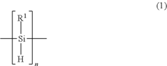
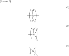
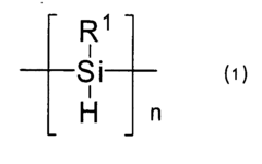
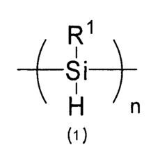
- Introducing a Si—H group into the polysilane main chain and bonding a hydrosilylatable compound with functional groups like hydroxyl, carboxyl, or epoxy groups, allowing for controlled hydrosilylation to enhance solubility and reactivity without complex steps or special apparatus.


Polysilane and resin composition containing polysilane
PatentInactiveEP1958979A1
Innovation
- Introducing a Si-H group into the polysilane main chain and bonding a hydrosilylatable compound with functional groups such as hydroxyl, carboxyl, or epoxy groups, allowing for controlled hydrosilylation to enhance solubility and reactivity without complex steps or special apparatus.

Environmental Impact of Polysilane
Polysilane, a class of silicon-based polymers, has gained significant attention in device design solutions due to its unique properties. However, its environmental impact is a crucial aspect that requires careful consideration. The production and use of polysilane materials can have both positive and negative effects on the environment.
One of the primary environmental benefits of polysilane is its potential to improve the efficiency of electronic devices. By enabling the development of more compact and energy-efficient components, polysilane-based devices can contribute to reduced energy consumption and, consequently, lower greenhouse gas emissions. This aligns with global efforts to combat climate change and promote sustainable technology development.
However, the synthesis of polysilane often involves the use of toxic precursors and solvents, which can pose environmental risks if not properly managed. The production process may generate hazardous waste that requires specialized treatment and disposal methods to prevent contamination of soil and water resources. Additionally, the energy-intensive nature of polysilane synthesis can contribute to increased carbon emissions if not powered by renewable energy sources.
The end-of-life management of polysilane-containing devices is another critical environmental consideration. As these materials become more prevalent in electronic products, proper recycling and disposal methods must be developed to prevent the release of potentially harmful substances into the environment. The silicon-based nature of polysilane may offer advantages in terms of recyclability compared to some organic polymers, but further research is needed to optimize recycling processes and minimize environmental impact.
Biodegradability is an area where polysilane materials face challenges. Unlike some organic polymers, polysilanes do not readily degrade in natural environments, which could lead to long-term accumulation in ecosystems if not properly managed. This persistence underscores the importance of developing effective recycling and recovery strategies for polysilane-based products.
On the other hand, the durability of polysilane materials can contribute to extended product lifespans, potentially reducing the frequency of device replacement and associated electronic waste generation. This longevity, when coupled with proper design for disassembly and recycling, could lead to more sustainable product lifecycles.
As research in polysilane technology progresses, there is growing interest in developing more environmentally friendly synthesis methods and exploring bio-based precursors. These efforts aim to reduce the environmental footprint of polysilane production while maintaining or enhancing its beneficial properties for device design. Furthermore, the integration of life cycle assessment methodologies in the development of polysilane-based technologies is crucial for comprehensively evaluating and mitigating their environmental impact.
Polysilane Commercialization Strategies
The commercialization of polysilane technology presents significant opportunities for device manufacturers and materials suppliers. As polysilanes demonstrate exceptional properties for advanced electronic and optoelectronic applications, strategic approaches are needed to successfully bring these materials to market.
A key commercialization strategy is to focus on high-value niche applications where polysilanes offer clear performance advantages. Areas such as organic light-emitting diodes (OLEDs), photovoltaics, and chemical sensors show particular promise. By targeting these specialized markets initially, companies can establish a foothold and demonstrate the unique capabilities of polysilane-based devices.
Partnerships between materials developers and device manufacturers will be crucial for accelerating commercialization. Collaborations can help align polysilane synthesis capabilities with specific device requirements, leading to optimized material formulations. Joint development agreements may also provide access to complementary technologies and expertise needed to create market-ready products.
Scaling up polysilane production while maintaining quality and reducing costs is another critical factor. Investments in advanced synthesis and purification processes will be necessary to achieve commercial viability. Exploring alternative precursor materials and synthesis routes could potentially lower production expenses and improve yields.
Intellectual property (IP) strategy will play a vital role in commercialization efforts. Companies should focus on building strong patent portfolios covering novel polysilane structures, synthesis methods, and device applications. Licensing agreements may also be leveraged to access key technologies or expand market reach.
Regulatory compliance and safety assessments must be prioritized as polysilanes move towards commercial production. Thorough toxicological studies and environmental impact analyses will be essential for gaining regulatory approvals and ensuring public acceptance of polysilane-based products.
Marketing and education initiatives will be necessary to raise awareness of polysilane technology among potential customers and end-users. Highlighting the unique properties and performance benefits of polysilanes compared to incumbent materials will be crucial for driving adoption in target markets.
As the technology matures, exploring opportunities for vertical integration along the value chain may become advantageous. This could involve polysilane producers expanding into device manufacturing or electronics companies developing in-house polysilane synthesis capabilities.
Ultimately, successful commercialization will require a multifaceted approach combining technological innovation, strategic partnerships, and market-focused development efforts. By addressing key challenges and capitalizing on the unique properties of polysilanes, companies can position themselves to capture value in this emerging field of advanced materials.
Unlock deeper insights with PatSnap Eureka Quick Research — get a full tech report to explore trends and direct your research. Try now!
Generate Your Research Report Instantly with AI Agent
Supercharge your innovation with PatSnap Eureka AI Agent Platform!