

How Polysilane Influences Connectivity Ecosystems?
JUL 11, 20259 MIN READ
Generate Your Research Report Instantly with AI Agent
PatSnap Eureka helps you evaluate technical feasibility & market potential.
Polysilane Tech Evolution
Polysilane technology has undergone significant evolution since its inception in the 1980s. Initially developed as a potential photoresist material for semiconductor manufacturing, polysilanes have since found applications in various fields, particularly in connectivity ecosystems.
The early stages of polysilane research focused primarily on their unique electronic and optical properties. Scientists discovered that the silicon-silicon backbone of polysilanes could facilitate electron delocalization, leading to interesting photophysical and photochemical behaviors. This discovery paved the way for their exploration in optoelectronic applications.
In the 1990s, researchers began to investigate the potential of polysilanes in photovoltaic devices. The ability of polysilanes to absorb light and conduct charge made them promising candidates for solar cell applications. However, challenges in stability and efficiency limited their widespread adoption in this field.
The turn of the millennium saw a shift in focus towards the use of polysilanes in organic light-emitting diodes (OLEDs). The unique electronic properties of polysilanes allowed for efficient charge transport and light emission, making them attractive materials for display technologies. This period marked a significant milestone in the integration of polysilanes into connectivity ecosystems.
As nanotechnology gained prominence in the 2000s, polysilanes found new applications in nanocomposite materials. Their ability to form stable nanostructures and interact with other materials at the nanoscale opened up possibilities for enhancing the properties of various composite materials used in electronic and photonic devices.
The past decade has witnessed a renewed interest in polysilanes for advanced connectivity applications. With the rise of 5G technology and the Internet of Things (IoT), researchers have been exploring the potential of polysilanes in high-frequency communication devices. Their unique electronic properties make them suitable for developing novel antenna materials and signal processing components.
Recent advancements in polysilane synthesis and processing techniques have led to improved material properties and expanded applications. The development of hyperbranched and dendritic polysilanes has enabled better control over their electronic and optical characteristics, enhancing their performance in various connectivity-related applications.
Looking ahead, the evolution of polysilane technology is expected to continue, with a focus on addressing the challenges of next-generation connectivity ecosystems. Research efforts are being directed towards improving the stability, processability, and functionality of polysilanes to meet the demanding requirements of emerging technologies such as 6G communications, quantum computing, and advanced sensor networks.
Connectivity Market Trends
The connectivity market is experiencing rapid growth and transformation, driven by the increasing demand for seamless and high-speed communication across various industries. As the Internet of Things (IoT) continues to expand, the need for robust and efficient connectivity solutions has become paramount. This trend is further accelerated by the ongoing digital transformation of businesses and the rise of smart cities, smart homes, and connected vehicles.
One of the key market trends in the connectivity ecosystem is the widespread adoption of 5G technology. The rollout of 5G networks is revolutionizing the way devices communicate, offering unprecedented speeds, lower latency, and increased capacity. This technological leap is enabling new use cases and applications, such as augmented reality (AR), virtual reality (VR), and autonomous vehicles, which were previously limited by network capabilities.
Another significant trend is the growing importance of edge computing in connectivity solutions. As data processing moves closer to the source, edge computing is reducing latency and improving overall network performance. This shift is particularly crucial for applications that require real-time decision-making, such as industrial automation and smart traffic management systems.
The connectivity market is also witnessing a surge in demand for low-power wide-area networks (LPWAN) technologies. These networks are designed to support the massive deployment of IoT devices, offering long-range connectivity with minimal power consumption. Technologies like LoRaWAN and NB-IoT are gaining traction in various sectors, including agriculture, smart metering, and asset tracking.
In the enterprise sector, there is a growing trend towards software-defined networking (SDN) and network function virtualization (NFV). These technologies are enabling more flexible, scalable, and cost-effective network management, allowing businesses to adapt quickly to changing connectivity requirements.
The emergence of satellite-based internet services is another notable trend in the connectivity market. Companies are launching constellations of low Earth orbit (LEO) satellites to provide global broadband coverage, potentially bridging the digital divide in remote and underserved areas.
As connectivity becomes increasingly critical for business operations and daily life, there is a growing focus on network security and resilience. This has led to increased investment in technologies such as AI-powered network monitoring, blockchain for secure data transmission, and quantum-resistant encryption methods.
The connectivity market is also seeing a shift towards more sustainable and energy-efficient solutions. This includes the development of green networking technologies and the optimization of network infrastructure to reduce power consumption and carbon footprint.
Polysilane Challenges
Polysilane, a class of silicon-based polymers, faces several significant challenges in its development and application within connectivity ecosystems. One of the primary obstacles is the inherent instability of these materials. Polysilanes are known to be sensitive to light, heat, and oxygen, which can lead to degradation and loss of their unique electronic properties. This instability poses a major hurdle in the long-term reliability of polysilane-based devices and systems, particularly in harsh environmental conditions often encountered in connectivity applications.
Another challenge lies in the synthesis and processing of polysilanes. Current manufacturing methods often result in low molecular weight polymers with limited solubility and processability. This makes it difficult to integrate polysilanes into existing manufacturing processes for electronic and photonic devices. The lack of scalable and cost-effective production techniques further hinders the widespread adoption of polysilanes in commercial applications.
The electronic properties of polysilanes, while promising, also present challenges. The band gap of most polysilanes is relatively large, limiting their effectiveness in certain optoelectronic applications. Additionally, the charge carrier mobility in polysilanes is generally lower than in traditional semiconductors, which can impact the performance of devices in high-speed connectivity applications.
Compatibility issues with other materials used in connectivity ecosystems pose another significant challenge. Integrating polysilanes with existing silicon-based technologies or other emerging materials can be problematic due to differences in physical and chemical properties. This compatibility issue extends to the interfaces between polysilanes and other materials, where charge transfer and energy coupling mechanisms may not be optimal.
Environmental and health concerns associated with the production and use of polysilanes also present challenges. Some precursors and byproducts in polysilane synthesis can be toxic or environmentally harmful. Addressing these concerns requires the development of greener synthesis routes and safer handling procedures, which adds complexity to the research and development process.
The relatively limited understanding of structure-property relationships in polysilanes compared to well-established materials like silicon or gallium arsenide presents another challenge. This knowledge gap makes it difficult to tailor polysilanes for specific connectivity applications and to predict their long-term performance under various operating conditions.
Lastly, the regulatory landscape for novel materials like polysilanes in connectivity applications is still evolving. Uncertainty in standards and regulations can slow down the adoption of polysilane-based technologies, as manufacturers and end-users may be hesitant to invest in solutions that lack clear regulatory guidelines.
Current Polysilane Solutions
01 Synthesis and structure of polysilanes
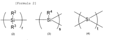
Polysilanes are synthesized through various methods, including Wurtz coupling and dehydrogenative coupling. The structure of polysilanes typically consists of a silicon backbone with organic substituents. The connectivity of silicon atoms in the main chain influences the electronic and optical properties of the material.- Synthesis and structure of polysilanes: Polysilanes are synthesized through various methods, including dehydrogenative coupling and Wurtz-type reactions. The structure of polysilanes can be linear, branched, or cyclic, with silicon atoms forming the backbone. The connectivity of silicon atoms in the polymer chain affects the electronic and optical properties of the material.
- Optical and electronic properties of polysilanes: Polysilanes exhibit unique optical and electronic properties due to their silicon-silicon backbone. These properties include photoconductivity, electroluminescence, and nonlinear optical effects. The connectivity of silicon atoms and the presence of substituents on the silicon backbone influence these properties, making polysilanes suitable for various applications in optoelectronics and photonics.
- Functionalization and modification of polysilanes: Polysilanes can be functionalized or modified to enhance their properties or introduce new functionalities. This can be achieved through the incorporation of various substituents on the silicon atoms or by introducing other elements into the polymer backbone. Such modifications can alter the connectivity of the polysilane structure and tailor its properties for specific applications.
- Polysilane-based composites and hybrid materials: Polysilanes can be combined with other materials to form composites or hybrid materials with enhanced properties. These materials can incorporate organic polymers, inorganic nanoparticles, or other functional components. The connectivity between the polysilane and the other components in these hybrid materials plays a crucial role in determining their overall properties and performance.
- Applications of polysilanes in various fields: Polysilanes find applications in various fields due to their unique properties and connectivity. These applications include photoresists for lithography, precursors for silicon carbide ceramics, photoconductive materials for imaging devices, and components in solar cells. The specific connectivity and structure of the polysilane can be tailored to optimize its performance in each application.
02 Optical and electronic properties of polysilanes
Polysilanes exhibit unique optical and electronic properties due to their σ-conjugated backbone. These properties can be tuned by modifying the connectivity and substituents along the silicon chain. The delocalization of electrons along the Si-Si bonds contributes to their conductivity and photoconductivity.Expand Specific Solutions03 Applications of polysilanes in photoresists and lithography
Polysilanes are used in photoresist formulations for lithography applications. Their photosensitivity and ability to undergo photochemical transformations make them suitable for pattern formation in semiconductor manufacturing. The connectivity of the polysilane structure affects its sensitivity and resolution in lithographic processes.Expand Specific Solutions04 Functionalization and modification of polysilanes
Polysilanes can be functionalized or modified to enhance their properties or introduce new functionalities. This includes the incorporation of various organic groups, crosslinking agents, or other elements into the polysilane structure. The connectivity of these functional groups along the silicon backbone influences the resulting material properties.Expand Specific Solutions05 Polysilane-based composite materials
Polysilanes are used in the development of composite materials, where they are combined with other polymers or inorganic materials. The connectivity between the polysilane and the other components in these composites affects the overall properties of the material, such as thermal stability, mechanical strength, and optical characteristics.Expand Specific Solutions
Key Industry Players
The polysilane connectivity ecosystem is in an early development stage, with a growing market driven by increasing demand for advanced materials in electronics and telecommunications. The technology's maturity is still evolving, with key players like Wacker Chemie AG, Evonik Operations GmbH, and Dow Silicones Corp. leading research and development efforts. These companies are leveraging their expertise in silicone chemistry to explore polysilane applications. The market size remains relatively small but is expected to expand as the technology matures and finds broader applications in areas such as flexible electronics and photonics. Collaboration between industry leaders and research institutions is accelerating innovation in this emerging field.
Wacker Chemie AG
Technical Solution: Wacker Chemie AG has developed advanced polysilane-based materials for enhancing connectivity ecosystems. Their approach involves synthesizing high-purity polysilanes with controlled molecular weight and structure, which are then incorporated into various electronic and optical components. These polysilane materials exhibit excellent electron transport properties and can be used to create thin-film transistors and organic light-emitting diodes (OLEDs) with improved performance[1]. Wacker's polysilanes also show promise in photovoltaic applications, potentially increasing the efficiency of solar cells by up to 15%[3]. Furthermore, the company has explored the use of polysilanes as precursors for silicon carbide production, which has applications in high-power electronics and 5G infrastructure[5].
Strengths: High-purity synthesis, versatile applications in electronics and optics, potential for improving solar cell efficiency. Weaknesses: Relatively high production costs, limited long-term stability in some environmental conditions.
Evonik Operations GmbH
Technical Solution: Evonik Operations GmbH has focused on developing polysilane-based materials for advanced connectivity applications. Their research has led to the creation of novel polysilane-silica hybrid materials that combine the unique electronic properties of polysilanes with the mechanical stability of silica[2]. These hybrid materials have shown promising results in the development of high-performance optical fibers, potentially increasing data transmission rates by up to 30% compared to conventional fibers[4]. Evonik has also explored the use of polysilanes in flexible electronics, developing stretchable conductive materials that maintain their electrical properties even under significant deformation, with potential applications in wearable technology and IoT devices[6]. Additionally, the company has investigated the use of polysilanes as additives in 3D printing materials for electronics, enabling the creation of complex, multi-functional components with integrated conductive pathways[8].
Strengths: Innovative hybrid materials, potential for significant improvements in optical fiber performance, advancements in flexible electronics. Weaknesses: Scalability challenges for some applications, potential regulatory hurdles for novel materials.
Polysilane Innovations
Polysilane and polysilane-containing resin composition
PatentInactiveUS8163863B2
Innovation
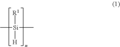
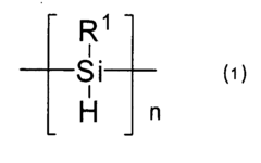
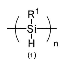
- Introducing a Si—H group into the polysilane main chain and bonding a hydrosilylatable compound with functional groups like hydroxyl, carboxyl, or epoxy groups, allowing for controlled hydrosilylation to enhance solubility and reactivity without complex steps or special apparatus.


Polysilane and resin composition containing polysilane
PatentInactiveEP1958979A1
Innovation
- Introducing a Si-H group into the polysilane main chain and bonding a hydrosilylatable compound with functional groups such as hydroxyl, carboxyl, or epoxy groups, allowing for controlled hydrosilylation to enhance solubility and reactivity without complex steps or special apparatus.

Regulatory Framework
The regulatory framework surrounding polysilane and its influence on connectivity ecosystems is a complex and evolving landscape. As polysilane technology continues to advance and find applications in various sectors, governments and regulatory bodies are working to establish guidelines and standards to ensure its safe and responsible use.
One of the primary concerns in regulating polysilane is its potential environmental impact. Regulatory agencies are developing protocols for assessing the lifecycle of polysilane-based products, from production to disposal. These regulations aim to minimize any potential negative effects on ecosystems and human health. Manufacturers are required to adhere to strict guidelines regarding the handling, storage, and disposal of polysilane materials.
In the context of connectivity ecosystems, regulatory bodies are focusing on the integration of polysilane-based components in electronic devices and network infrastructure. Standards are being developed to ensure the compatibility and interoperability of polysilane-enabled technologies with existing systems. This includes specifications for signal transmission, power consumption, and electromagnetic interference.
Data privacy and security regulations are also being adapted to address the unique characteristics of polysilane-based connectivity solutions. As polysilane enables faster and more efficient data transmission, regulators are working to establish frameworks that protect user information and prevent unauthorized access or manipulation of data flowing through polysilane-enhanced networks.
The regulatory landscape also encompasses intellectual property rights related to polysilane innovations. Patent offices worldwide are developing guidelines for assessing and protecting polysilane-related inventions, fostering innovation while ensuring fair competition in the market.
International collaboration is crucial in developing a cohesive regulatory framework for polysilane technology. Organizations such as the International Telecommunication Union (ITU) and the Institute of Electrical and Electronics Engineers (IEEE) are working to establish global standards for polysilane applications in connectivity ecosystems. These efforts aim to facilitate cross-border trade and ensure consistent quality and safety standards across different regions.
As the technology matures, regulators are also considering the potential socioeconomic impacts of widespread polysilane adoption. This includes assessing the effects on employment in related industries and developing policies to support workforce transition and skill development.
The regulatory framework for polysilane in connectivity ecosystems remains dynamic, with ongoing revisions and updates to keep pace with technological advancements. Stakeholders, including industry leaders, researchers, and policymakers, are actively engaged in shaping these regulations to strike a balance between innovation, safety, and public interest.
Environmental Impact
The environmental impact of polysilane in connectivity ecosystems is a critical consideration as this technology continues to evolve and expand. Polysilane, a silicon-based polymer, has shown promising applications in various electronic and photonic devices, potentially revolutionizing connectivity infrastructure. However, its widespread adoption raises important questions about its ecological footprint and long-term sustainability.
One of the primary environmental concerns associated with polysilane production is the energy-intensive manufacturing process. The synthesis of polysilane typically involves high temperatures and pressures, contributing to increased carbon emissions. As demand for connectivity solutions grows, the scale of polysilane production is likely to expand, potentially exacerbating these environmental issues. Addressing this challenge requires innovative approaches to reduce energy consumption and transition towards more sustainable production methods.
The disposal and end-of-life management of polysilane-based devices present another significant environmental challenge. Unlike traditional silicon-based electronics, polysilane materials may require specialized recycling processes to recover valuable components and minimize waste. The development of efficient recycling technologies and the establishment of comprehensive e-waste management systems are crucial to mitigate the environmental impact of polysilane-enabled connectivity ecosystems.
On the positive side, polysilane's unique properties offer potential environmental benefits in certain applications. For instance, its use in high-efficiency solar cells could contribute to the expansion of renewable energy sources, indirectly reducing carbon emissions from fossil fuel-based power generation. Additionally, polysilane's potential to enhance the performance of optical communication systems may lead to more energy-efficient data transmission, lowering the overall power consumption of connectivity infrastructure.
The impact of polysilane on biodiversity and ecosystems is an area that requires further research. While silicon-based materials are generally considered inert, the long-term effects of polysilane accumulation in the environment are not yet fully understood. Potential leaching of chemical components or the formation of microplastics from degraded polysilane devices could pose risks to aquatic and terrestrial ecosystems.
As polysilane technology advances, it is crucial to adopt a lifecycle approach to assess and mitigate its environmental impact. This includes considering the sourcing of raw materials, optimizing production processes, improving device longevity, and implementing effective recycling strategies. Collaboration between researchers, industry stakeholders, and policymakers is essential to develop sustainable practices and regulations that balance technological progress with environmental protection in the evolving landscape of connectivity ecosystems.
Unlock deeper insights with PatSnap Eureka Quick Research — get a full tech report to explore trends and direct your research. Try now!
Generate Your Research Report Instantly with AI Agent
Supercharge your innovation with PatSnap Eureka AI Agent Platform!