

Understanding Polysilane’s Unique Deployment in Electronics
JUL 11, 20259 MIN READ
Generate Your Research Report Instantly with AI Agent
PatSnap Eureka helps you evaluate technical feasibility & market potential.
Polysilane Evolution
Polysilanes have undergone a remarkable evolution since their initial discovery in the mid-20th century. The journey of these unique silicon-based polymers in the field of electronics began with the recognition of their potential as semiconducting materials. Early research focused on understanding the fundamental properties of polysilanes, particularly their sigma-conjugation along the silicon backbone, which contributes to their electronic and optical characteristics.
The 1980s marked a significant milestone in polysilane evolution, as researchers began to explore their application in photoresists for microelectronics. This period saw the development of various synthesis methods, enabling the creation of polysilanes with diverse structures and properties. The ability to fine-tune the electronic properties of polysilanes by modifying their side chains opened up new possibilities for their use in electronic devices.
As the field progressed into the 1990s and early 2000s, the focus shifted towards enhancing the stability and processability of polysilanes. This era witnessed the emergence of novel polysilane architectures, including hyperbranched and dendritic structures, which offered improved solubility and film-forming properties. These advancements paved the way for the integration of polysilanes into a wider range of electronic applications, such as organic light-emitting diodes (OLEDs) and photovoltaic cells.
The turn of the millennium brought about a renewed interest in polysilanes as precursors for silicon carbide (SiC) and silicon nitride (Si3N4) ceramics. This application leveraged the unique thermal decomposition properties of polysilanes, allowing for the fabrication of high-performance ceramic materials for electronic packaging and thermal management in advanced electronic systems.
Recent years have seen a surge in research focused on nanostructured polysilanes. The ability to control the morphology of polysilanes at the nanoscale has led to the development of nanofibers, nanoparticles, and thin films with enhanced electronic properties. These nanostructured materials have shown promise in applications such as chemical sensors, memory devices, and flexible electronics.
The evolution of polysilanes in electronics has also been marked by advancements in characterization techniques. The development of sophisticated spectroscopic and microscopic methods has enabled researchers to gain deeper insights into the structure-property relationships of polysilanes, facilitating more targeted design and optimization of these materials for specific electronic applications.
Looking ahead, the trajectory of polysilane evolution points towards their integration with other emerging materials and technologies. The potential synergies between polysilanes and two-dimensional materials, such as graphene and transition metal dichalcogenides, are being explored for next-generation electronic devices. Additionally, the role of polysilanes in the burgeoning field of organic electronics continues to expand, with ongoing research into their use in organic field-effect transistors (OFETs) and organic photovoltaics (OPVs).
Market Demand Analysis
The market demand for polysilane in electronics is experiencing significant growth, driven by the material's unique properties and potential applications. Polysilane, a silicon-based polymer, offers a combination of electrical conductivity and optical properties that make it particularly attractive for various electronic components and devices.
In the semiconductor industry, polysilane is gaining traction as a potential alternative to traditional silicon-based materials. Its ability to form thin films with controllable electronic properties has sparked interest in its use for next-generation transistors and memory devices. The increasing demand for smaller, more efficient electronic components is fueling research and development efforts to incorporate polysilane into advanced semiconductor manufacturing processes.
The display technology sector is another area where polysilane is showing promise. Its photoluminescent properties make it an attractive candidate for use in organic light-emitting diodes (OLEDs) and other display technologies. As the global demand for high-quality, energy-efficient displays continues to rise, polysilane-based materials could play a crucial role in advancing display performance and reducing power consumption.
In the field of photovoltaics, polysilane is being explored for its potential to enhance the efficiency of solar cells. Its unique electronic structure and light-absorbing properties could lead to the development of more cost-effective and higher-performing solar energy solutions. This aligns with the growing global focus on renewable energy sources and the push for more sustainable technologies.
The emerging field of flexible electronics is also driving demand for polysilane-based materials. The polymer's ability to be processed into flexible, thin films makes it an ideal candidate for applications such as wearable devices, flexible displays, and electronic skin. As the market for flexible and stretchable electronics expands, polysilane is well-positioned to meet the increasing demand for materials that can withstand bending and stretching while maintaining electronic functionality.
Furthermore, the automotive industry is showing interest in polysilane for its potential applications in advanced sensors and electronic systems. As vehicles become more electrified and autonomous, the need for innovative materials that can enhance performance and reliability is growing. Polysilane's unique properties could contribute to the development of more robust and efficient automotive electronics.
While the market demand for polysilane in electronics is promising, it is important to note that the technology is still in its early stages of commercialization. Ongoing research and development efforts are focused on optimizing polysilane synthesis, improving its stability, and enhancing its integration with existing manufacturing processes. As these challenges are addressed, the market demand is expected to accelerate, potentially leading to widespread adoption across various electronic applications.
Technical Challenges
Polysilane, a unique class of silicon-based polymers, presents several technical challenges in its deployment for electronic applications. One of the primary obstacles is the material's inherent instability when exposed to air and moisture. This sensitivity can lead to rapid degradation of the polymer structure, significantly impacting its electrical and optical properties. Researchers and engineers must develop effective encapsulation techniques or chemical modifications to enhance the stability of polysilane-based devices in ambient conditions.
Another significant challenge lies in the precise control of polysilane's molecular weight and polydispersity. These factors greatly influence the material's electronic properties, including charge carrier mobility and energy band structure. Achieving consistent and reproducible synthesis of polysilanes with desired molecular characteristics remains a complex task, requiring advanced polymerization techniques and stringent quality control measures.
The integration of polysilanes into existing electronic manufacturing processes poses additional hurdles. Traditional semiconductor fabrication methods may not be directly applicable to polysilane-based devices due to differences in material properties and processing requirements. Developing compatible deposition techniques, patterning methods, and integration strategies that preserve the unique properties of polysilanes while ensuring compatibility with conventional electronics is crucial for widespread adoption.
Thermal management is another critical challenge in polysilane-based electronics. The material's relatively low thermal conductivity can lead to heat accumulation in devices, potentially affecting performance and longevity. Innovative cooling solutions and thermal management strategies need to be devised to address this limitation, especially for high-power or densely packed electronic applications.
Furthermore, the optimization of charge transport mechanisms in polysilane-based devices remains an ongoing challenge. While polysilanes exhibit interesting electronic properties, including potential for high charge carrier mobility, translating these properties into practical device performance requires a deep understanding of charge injection, transport, and extraction processes at various interfaces within the device structure.
Lastly, the environmental impact and toxicity of polysilanes and their precursors present both technical and regulatory challenges. Developing eco-friendly synthesis routes, minimizing the use of hazardous materials, and ensuring safe disposal or recycling of polysilane-based electronics are essential considerations for the sustainable deployment of this technology in the electronics industry.
Current Polysilane Apps
01 Synthesis and properties of polysilanes
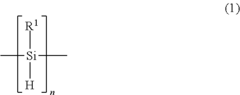
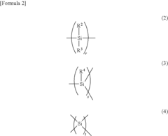
Polysilanes are synthesized through various methods and exhibit unique properties. They are silicon-based polymers with a Si-Si backbone, which can be modified with different substituents. These materials have applications in electronics, optics, and materials science due to their electronic and optical properties.- Synthesis and properties of polysilanes: Polysilanes are synthesized through various methods and exhibit unique properties. These silicon-based polymers have applications in electronics, optics, and materials science due to their electronic and optical characteristics. The synthesis and modification of polysilanes can be tailored to achieve specific properties for different applications.
- Polysilanes as precursors for silicon-based materials: Polysilanes serve as precursors for the production of various silicon-based materials. They can be converted into silicon carbide, silicon nitride, or pure silicon through thermal decomposition or other processes. This makes polysilanes valuable in the fabrication of ceramics, semiconductors, and other advanced materials.
- Applications of polysilanes in photoresists and lithography: Polysilanes find applications in photoresists and lithography processes. Their photosensitive properties make them suitable for use in the production of microelectronic devices and other patterned structures. Polysilane-based photoresists can offer high resolution and good etching resistance.
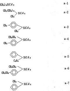
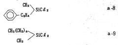
- Functionalization and modification of polysilanes: Polysilanes can be functionalized and modified to enhance their properties or introduce new functionalities. This includes the incorporation of various side groups, crosslinking, or copolymerization with other monomers. Such modifications allow for the tailoring of polysilanes for specific applications or to improve their processability and stability.
- Polysilanes in optical and electronic applications: The unique electronic structure of polysilanes makes them suitable for various optical and electronic applications. They can be used in organic light-emitting diodes (OLEDs), photovoltaic devices, and as charge transport materials. The σ-conjugation along the silicon backbone contributes to their interesting optoelectronic properties.
02 Applications in photoresist and lithography
Polysilanes are used in photoresist formulations and lithography processes. They exhibit high sensitivity to UV light and can undergo photochemical reactions, making them suitable for patterning and imaging applications in the semiconductor industry.Expand Specific Solutions03 Polysilane-based coatings and films
Polysilanes can be used to create thin films and coatings with various functional properties. These films can be applied to surfaces to impart characteristics such as improved durability, optical properties, or electronic conductivity.Expand Specific Solutions04 Modification and functionalization of polysilanes
Polysilanes can be modified and functionalized to enhance their properties or introduce new functionalities. This includes the incorporation of various organic groups, metal atoms, or other elements to tailor the material's characteristics for specific applications.Expand Specific Solutions05 Polysilane-based composites and hybrid materials
Polysilanes can be combined with other materials to create composites or hybrid materials with enhanced properties. These composites may exhibit improved mechanical, thermal, or electrical characteristics, making them suitable for a wide range of applications in advanced materials science.Expand Specific Solutions
Key Industry Players
The competitive landscape for polysilane deployment in electronics is in an early growth stage, with a relatively small but expanding market size. The technology is still maturing, with key players like JSR Corp., Wacker Chemie AG, and Dow Silicones Corp. leading research and development efforts. Universities such as Hangzhou Normal University and Shanghai University are contributing to fundamental research, while companies like Canon Inc. and Fujitsu Ltd. are exploring practical applications. As the technology advances, collaborations between academic institutions and industry leaders are likely to drive innovation and commercialization in this emerging field.
Wacker Chemie AG
Technical Solution: Wacker Chemie AG has developed advanced polysilane materials for electronics applications. Their approach involves synthesizing high-purity polysilanes with controlled molecular weights and structures. These materials are used as precursors for silicon-based thin films in electronic devices. Wacker's polysilanes can be processed at lower temperatures compared to traditional silicon precursors, enabling their use on flexible substrates[1]. The company has also developed UV-curable polysilane formulations that can be patterned using photolithography for microelectronics applications[2]. Additionally, Wacker has explored the use of polysilanes as electron-transport materials in organic light-emitting diodes (OLEDs), leveraging their unique electronic properties[3].
Strengths: High-purity materials, low-temperature processing, versatility for various electronic applications. Weaknesses: May have higher production costs compared to traditional silicon precursors, limited commercial adoption in some areas.
Toray Industries, Inc.
Technical Solution: Toray Industries has developed proprietary polysilane materials and processing techniques for advanced electronic applications. Their approach focuses on creating ultra-thin polysilane films with precisely controlled thicknesses down to the nanometer scale[1]. These films are used as interlayer dielectrics in semiconductor devices, offering improved insulation properties and reduced signal interference. Toray has also explored the use of polysilanes as resist materials for next-generation lithography processes, leveraging their high etch resistance and patterning capabilities[2]. Additionally, the company has developed polysilane-based coatings for flexible electronics, providing both barrier properties and electrical functionality[3].
Strengths: Expertise in ultra-thin film formation, integration with existing semiconductor processes, diverse application range. Weaknesses: May face competition from established materials in some applications, potential scalability challenges for some specialized formulations.
Core Polysilane Patents
Polysilane and polysilane-containing resin composition
PatentInactiveUS8163863B2
Innovation
- Introducing a Si—H group into the polysilane main chain and bonding a hydrosilylatable compound with functional groups like hydroxyl, carboxyl, or epoxy groups, allowing for controlled hydrosilylation to enhance solubility and reactivity without complex steps or special apparatus.


Novel polysilane composition
PatentWO1991005018A1
Innovation
- A novel polysilane composition with a weight-average molecular weight of 6,000 to 2,000,000, where all substituents and terminal groups are substituted with specific organic groups without oxygen, combined with an acceptor or donor level former, enhancing solubility, film-forming ability, and structural integrity.
Environmental Impact
The deployment of polysilane in electronics has significant environmental implications that warrant careful consideration. Polysilane, a silicon-based polymer, offers unique properties that make it attractive for various electronic applications. However, its production, use, and disposal can have both positive and negative impacts on the environment.
From a production standpoint, the synthesis of polysilane typically involves energy-intensive processes and the use of potentially hazardous chemicals. This raises concerns about the carbon footprint and potential environmental contamination associated with its manufacturing. However, ongoing research is focused on developing more environmentally friendly synthesis methods, such as using renewable energy sources and exploring green chemistry approaches to reduce the overall environmental impact.
In terms of its application in electronics, polysilane's unique properties can contribute to the development of more energy-efficient devices. For instance, its use in organic light-emitting diodes (OLEDs) and photovoltaic cells can lead to improved energy conversion efficiency, potentially reducing overall energy consumption in electronic devices. This aligns with global efforts to minimize energy usage and combat climate change.
The durability and stability of polysilane-based electronic components may also have positive environmental implications. Longer-lasting devices could reduce electronic waste generation, a growing environmental concern. However, this benefit must be balanced against the potential challenges in recycling or disposing of polysilane-containing electronics at the end of their life cycle.
Polysilane's biodegradability is an area of ongoing research. While some studies suggest that certain polysilane derivatives can degrade under specific environmental conditions, the long-term environmental fate of these materials in various ecosystems remains uncertain. This highlights the need for comprehensive life cycle assessments to fully understand the environmental impact of polysilane-based electronics from production to disposal.
Water and soil contamination risks associated with polysilane production and disposal also require careful management. Proper handling and treatment of waste materials are essential to prevent potential environmental hazards. Additionally, the potential release of nanoparticles during the wear and tear of polysilane-containing devices raises concerns about their impact on ecosystems and human health, necessitating further research and regulatory considerations.
As the electronics industry continues to explore and expand the use of polysilane, it is crucial to adopt a holistic approach to environmental stewardship. This includes investing in cleaner production technologies, optimizing device efficiency to reduce energy consumption, and developing effective recycling and disposal methods for polysilane-based electronics. Collaborative efforts between researchers, manufacturers, and policymakers will be essential in maximizing the benefits of polysilane while minimizing its environmental footprint.
Scalability Prospects
The scalability prospects for polysilane in electronics are promising, driven by its unique properties and potential for large-scale production. As research progresses, the ability to synthesize polysilane materials with consistent quality and in larger quantities is improving. This scalability is crucial for the widespread adoption of polysilane in various electronic applications.
One of the key factors contributing to polysilane's scalability is the development of more efficient synthesis methods. Traditional methods often resulted in low yields and limited molecular weight control. However, recent advancements in catalytic polymerization and controlled radical polymerization techniques have significantly enhanced the production capabilities. These improved methods allow for better control over the molecular structure and properties of polysilanes, making them more suitable for large-scale manufacturing processes.
The integration of polysilane into existing semiconductor fabrication processes is another important aspect of its scalability. As the electronics industry continues to seek alternatives to traditional silicon-based technologies, polysilane offers a compatible and potentially more versatile option. Its ability to be processed using similar techniques to those employed in current semiconductor manufacturing lines reduces the barriers to adoption and scaling.
Furthermore, the versatility of polysilane in terms of its electronic properties opens up possibilities for scalable applications across various electronic devices. From flexible displays to high-performance transistors, the adaptability of polysilane allows for its integration into diverse product lines. This versatility supports economies of scale, as manufacturers can potentially use similar production processes for multiple applications.
The growing interest in organic electronics and printed electronics also bodes well for polysilane's scalability prospects. These emerging fields require materials that can be easily processed and deposited over large areas, characteristics that polysilane possesses. As these technologies mature and move towards commercial production, the demand for scalable polysilane production is likely to increase.
However, challenges remain in achieving full-scale industrial production of polysilane for electronics. Issues such as long-term stability, environmental sensitivity, and cost-effective purification processes need to be addressed. Ongoing research and development efforts are focused on overcoming these hurdles, with promising results in areas such as encapsulation techniques and purification methods.
Unlock deeper insights with PatSnap Eureka Quick Research — get a full tech report to explore trends and direct your research. Try now!
Generate Your Research Report Instantly with AI Agent
Supercharge your innovation with PatSnap Eureka AI Agent Platform!