Innovations in Polysilane for Digital Circuit Applications
JUL 11, 20259 MIN READ
Generate Your Research Report Instantly with AI Agent
PatSnap Eureka helps you evaluate technical feasibility & market potential.
Polysilane Evolution and Objectives
Polysilane, a class of silicon-based polymers, has undergone significant evolution since its discovery in the mid-20th century. Initially synthesized as a curiosity in organosilicon chemistry, polysilanes have gradually emerged as promising materials for various applications, including digital circuits. The development of polysilanes has been driven by the continuous pursuit of novel materials with enhanced electronic properties and processability.
The early stages of polysilane research focused primarily on understanding their unique electronic structure and optical properties. As silicon-silicon backbone polymers, polysilanes exhibit σ-electron delocalization, which contributes to their semiconducting behavior. This characteristic sparked interest in their potential for electronic applications, including digital circuits.
Throughout the 1980s and 1990s, significant advancements were made in polysilane synthesis and characterization. Researchers explored various methods to control the molecular weight, polydispersity, and side-chain functionalization of polysilanes. These efforts aimed to tailor the electronic and physical properties of polysilanes for specific applications, including their potential use in digital circuits.
The turn of the millennium saw an increased focus on the application of polysilanes in electronic devices. Researchers began investigating their potential as active materials in field-effect transistors, photovoltaic cells, and other electronic components. The unique combination of processability and electronic properties made polysilanes an attractive alternative to traditional inorganic semiconductors in certain applications.
In recent years, the objectives of polysilane research for digital circuit applications have become more refined and targeted. One primary goal is to enhance the charge carrier mobility of polysilanes to improve their performance in transistor-based devices. This involves optimizing the molecular structure and morphology of polysilane films to facilitate efficient charge transport.
Another critical objective is to improve the stability and reliability of polysilane-based electronic components. This includes addressing issues such as oxidative degradation and thermal stability, which are crucial for ensuring the long-term performance of digital circuits. Researchers are exploring various strategies, including the incorporation of stabilizing additives and the development of protective coatings.
The integration of polysilanes with existing silicon-based technologies is also a key focus area. As the semiconductor industry continues to face challenges in scaling down traditional silicon devices, polysilanes offer potential solutions for certain niche applications or as complementary materials in hybrid organic-inorganic systems.
Looking forward, the objectives of polysilane research for digital circuit applications include further improving their electronic properties, enhancing their compatibility with established fabrication processes, and exploring novel device architectures that can leverage the unique characteristics of these materials. The ultimate goal is to develop polysilane-based digital circuits that offer advantages in terms of cost, flexibility, or functionality compared to conventional semiconductor technologies.
Digital Circuit Market Analysis
The digital circuit market has experienced significant growth in recent years, driven by the increasing demand for advanced electronic devices and systems across various industries. This market encompasses a wide range of applications, including consumer electronics, automotive, industrial automation, and telecommunications. The global digital circuit market was valued at approximately $78 billion in 2020 and is projected to reach $120 billion by 2025, with a compound annual growth rate (CAGR) of 9.0% during the forecast period.
One of the key factors driving market growth is the rapid adoption of Internet of Things (IoT) devices and smart technologies. As more devices become interconnected and require sophisticated processing capabilities, the demand for advanced digital circuits continues to rise. Additionally, the ongoing transition to 5G networks and the increasing popularity of artificial intelligence and machine learning applications are further fueling market expansion.
The automotive sector has emerged as a significant contributor to the digital circuit market, with the growing integration of advanced driver assistance systems (ADAS) and autonomous driving technologies. The increasing electrification of vehicles and the incorporation of infotainment systems have also boosted the demand for digital circuits in this sector.
In the consumer electronics segment, smartphones, tablets, and wearable devices remain major drivers of market growth. The continuous evolution of these devices, with enhanced processing power and functionality, necessitates more advanced digital circuits. The gaming industry, particularly with the rise of virtual reality and augmented reality technologies, has also become a significant consumer of digital circuits.
The industrial automation sector is another key market for digital circuits, as manufacturers increasingly adopt smart factory solutions and Industry 4.0 technologies. The need for real-time data processing, machine-to-machine communication, and advanced control systems has led to a surge in demand for digital circuits in this sector.
Geographically, Asia-Pacific dominates the digital circuit market, accounting for the largest market share. This is primarily due to the presence of major semiconductor manufacturers and electronic device producers in countries like China, South Korea, and Taiwan. North America and Europe follow closely, driven by technological advancements and the presence of key industry players.
Looking ahead, the digital circuit market is expected to continue its growth trajectory, with emerging technologies such as quantum computing and neuromorphic computing potentially revolutionizing the field. The ongoing miniaturization of electronic components and the push for more energy-efficient solutions are likely to shape the future of digital circuit design and manufacturing.
Polysilane Challenges in Digital Circuits
Polysilanes have emerged as promising materials for digital circuit applications, yet they face several significant challenges that hinder their widespread adoption. One of the primary obstacles is the inherent instability of polysilanes under certain conditions, particularly when exposed to ultraviolet light or elevated temperatures. This instability can lead to degradation of the material's electronic properties, potentially compromising the reliability and longevity of digital circuits incorporating polysilanes.
Another critical challenge lies in the difficulty of achieving precise control over the molecular weight and polydispersity of polysilanes during synthesis. This lack of control can result in inconsistent electrical properties across batches, making it challenging to manufacture digital circuits with reproducible performance characteristics. The variability in molecular structure also impacts the charge carrier mobility within the material, which is crucial for high-speed digital applications.
The integration of polysilanes into existing semiconductor manufacturing processes presents yet another hurdle. Traditional silicon-based fabrication techniques may not be directly applicable to polysilane materials, necessitating the development of new processing methods and equipment. This adaptation requires significant investment in research and development, as well as potential retooling of manufacturing facilities.
Furthermore, the environmental sensitivity of polysilanes poses challenges in terms of device encapsulation and packaging. Exposure to oxygen or moisture can alter the electronic properties of polysilanes, potentially leading to device failure or performance degradation over time. Developing effective barrier materials and encapsulation techniques that are compatible with polysilane-based devices is crucial for ensuring their long-term stability and reliability in real-world applications.
The relatively low charge carrier mobility of polysilanes compared to traditional semiconductors like silicon is another significant limitation. While polysilanes offer unique properties such as solution processability and flexibility, their lower mobility can restrict their use in high-performance digital circuits that require rapid switching speeds. Overcoming this limitation may require novel device architectures or doping strategies to enhance charge transport within polysilane-based structures.
Lastly, the cost-effectiveness of polysilane-based digital circuits remains a challenge. While polysilanes offer potential advantages in terms of processing and flexibility, the current production costs and scalability issues make it difficult to compete with well-established silicon-based technologies. Addressing these economic barriers will be crucial for the widespread adoption of polysilanes in commercial digital circuit applications.
Current Polysilane Solutions for Digital Circuits
01 Synthesis and properties of polysilanes
Polysilanes are silicon-based polymers with unique electronic and optical properties. They can be synthesized through various methods, including Wurtz coupling of dichlorosilanes. These polymers exhibit interesting characteristics such as photoconductivity and photoluminescence, making them suitable for various applications in electronics and optics.- Synthesis and properties of polysilanes: Polysilanes are silicon-based polymers with unique electronic and optical properties. They can be synthesized through various methods, including Wurtz coupling of dichlorosilanes. These polymers exhibit interesting characteristics such as photoconductivity and photoluminescence, making them suitable for various applications in electronics and optics.
- Applications of polysilanes in photoresists and lithography: Polysilanes are utilized in photoresist compositions for lithography processes. They can act as photosensitive materials or as additives to enhance the performance of photoresists. The unique properties of polysilanes, such as their ability to undergo photochemical reactions, make them valuable in the fabrication of microelectronic devices and other patterning applications.
- Polysilane-based thin films and coatings: Polysilanes can be used to create thin films and coatings with specific properties. These films can be deposited through various methods, including spin-coating and chemical vapor deposition. The resulting coatings may exhibit properties such as high thermal stability, optical transparency, or electrical conductivity, making them suitable for applications in electronics, optics, and protective coatings.
- Functionalization and modification of polysilanes: Polysilanes can be functionalized or modified to enhance their properties or introduce new functionalities. This can involve the incorporation of various organic groups or other elements into the polymer backbone or as side chains. Such modifications can lead to improved solubility, altered optical properties, or enhanced reactivity, expanding the range of potential applications for polysilanes.
- Polysilanes as precursors for silicon-based materials: Polysilanes can serve as precursors for the production of various silicon-based materials. Through controlled thermal decomposition or other conversion processes, polysilanes can be transformed into silicon carbide, silicon nitride, or other ceramic materials. This approach allows for the creation of advanced materials with tailored properties for applications in high-temperature environments or as structural components.
02 Applications of polysilanes in coatings and films
Polysilanes can be used to create functional coatings and films with specific properties. These materials can be applied to various substrates to impart characteristics such as improved adhesion, chemical resistance, or optical properties. The unique structure of polysilanes allows for the development of thin films with controlled thickness and composition.Expand Specific Solutions03 Polysilanes in photoresist materials
Polysilanes have found applications in photoresist materials for semiconductor manufacturing. Their photosensitivity and ability to form stable patterns make them suitable for lithography processes. These materials can be used to create high-resolution patterns for the fabrication of microelectronic devices.Expand Specific Solutions04 Modification and functionalization of polysilanes
Polysilanes can be modified and functionalized to enhance their properties or introduce new functionalities. This can involve the incorporation of various organic groups or the creation of copolymers with other materials. Such modifications allow for the tailoring of polysilanes for specific applications or to improve their compatibility with other materials.Expand Specific Solutions05 Polysilanes in electronic and optoelectronic devices
The unique electronic properties of polysilanes make them suitable for use in various electronic and optoelectronic devices. They can be used as charge transport materials, light-emitting components, or as part of solar cell structures. The ability to tune their properties through structural modifications allows for optimization in different device architectures.Expand Specific Solutions
Key Players in Polysilane Research
The field of polysilane innovations for digital circuit applications is in a nascent stage, with significant potential for growth. The market size is relatively small but expanding rapidly as researchers explore novel applications in semiconductor technology. The technical maturity is still developing, with key players like JSR Corp., Dexerials Corp., and Wacker Chemie AG leading research efforts. These companies are investing in R&D to enhance polysilane properties for improved conductivity and stability in digital circuits. While not yet mainstream, polysilane-based technologies are gaining traction in niche electronic applications, with industry experts predicting substantial market expansion in the coming years as manufacturing processes are refined and commercial viability increases.
Fujitsu Ltd.
Technical Solution: Fujitsu has made significant strides in polysilane-based digital circuit applications. Their research focuses on developing polysilane-organic hybrid materials that combine the high charge carrier mobility of polysilanes with the flexibility and processability of organic semiconductors[5]. Fujitsu's approach involves incorporating polysilane segments into organic polymer backbones, resulting in materials with tunable electronic properties[6]. These hybrid materials have been successfully used to fabricate organic field-effect transistors (OFETs) with improved performance and stability compared to traditional organic semiconductors[7]. Fujitsu has also explored the use of polysilane-based materials in memory devices, demonstrating potential for high-density, non-volatile memory applications[8].
Strengths: Hybrid material approach, improved device performance, and potential for diverse applications. Weaknesses: Complexity of material synthesis and potential scalability challenges.
Wacker Chemie AG
Technical Solution: Wacker Chemie AG has developed innovative polysilane materials for digital circuit applications. Their approach involves synthesizing high-purity polysilanes with controlled molecular weight and narrow polydispersity[1]. These materials exhibit enhanced electrical conductivity and charge carrier mobility, making them suitable for use in thin-film transistors and other electronic components[2]. Wacker's polysilanes are processed using solution-based techniques, allowing for low-cost, large-area fabrication of flexible electronic devices[3]. The company has also developed crosslinkable polysilanes that can be patterned using photolithography, enabling the creation of complex circuit structures with high resolution[4].
Strengths: High-purity materials, controlled properties, solution processability, and compatibility with existing fabrication techniques. Weaknesses: Potential stability issues under prolonged exposure to light or heat, and limited commercial-scale production experience.
Breakthrough Polysilane Innovations
Polysilane production process
PatentInactiveUS20110158886A1
Innovation
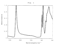
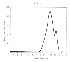
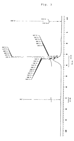
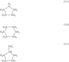
- A polysilane production process using a binuclear metal complex catalyst at room temperature and 1 atm to polymerize silane compounds, eliminating the need for large-scale equipment and enabling efficient polysilane synthesis under mild conditions.
Photoluminescent and/or electroluminescent material, method for production and use thereof and component comprising such a material
PatentWO2013068490A1
Innovation
- Development of polysilanes with stilbene and styrene units that are crosslinked to form stable, moisture-resistant materials with enhanced luminescence efficiency, suitable for use in optoelectronic components.
Environmental Impact of Polysilane
The environmental impact of polysilane in digital circuit applications is a crucial consideration as the semiconductor industry continues to evolve. Polysilanes, being silicon-based polymers, offer unique properties that make them attractive for various electronic applications. However, their production, use, and disposal can have significant environmental implications.
The manufacturing process of polysilanes involves the use of energy-intensive methods and potentially hazardous chemicals. The synthesis often requires high temperatures and pressures, contributing to increased energy consumption and associated carbon emissions. Additionally, the use of chlorinated solvents and other reactive compounds in the production process can lead to the generation of harmful by-products and waste streams that require careful management and disposal.
During the operational phase of digital circuits incorporating polysilane-based components, the environmental impact is generally minimal. Polysilanes exhibit excellent stability and durability, which can contribute to longer-lasting electronic devices and potentially reduce electronic waste. However, the end-of-life disposal of polysilane-containing electronics presents challenges similar to those of conventional semiconductor materials.
The recycling and disposal of polysilane-based electronic components require specialized processes to prevent the release of potentially harmful substances into the environment. Improper disposal can lead to soil and water contamination, as well as the release of volatile organic compounds (VOCs) into the atmosphere. Developing efficient recycling methods for polysilane-containing devices is crucial to mitigate these environmental risks and promote a circular economy in the electronics industry.
On a positive note, the unique properties of polysilanes, such as their photosensitivity and electrical conductivity, offer opportunities for developing more energy-efficient electronic devices. This could potentially lead to reduced power consumption in digital circuits, indirectly contributing to lower environmental impact during the use phase of electronic products.
Research into green chemistry approaches for polysilane synthesis is ongoing, aiming to develop more environmentally friendly production methods. These efforts focus on reducing the use of hazardous solvents, exploring room-temperature synthesis routes, and investigating bio-based precursors for polysilane production. Such advancements could significantly reduce the environmental footprint of polysilane manufacturing in the future.
As the demand for more advanced and miniaturized electronic devices grows, the environmental impact of materials like polysilanes becomes increasingly important. Balancing the technological benefits with environmental considerations will be crucial for the sustainable development of the semiconductor industry. This necessitates a holistic approach, encompassing cleaner production methods, efficient use of resources, and effective end-of-life management strategies for polysilane-based electronic components.
Polysilane Manufacturing Processes
Polysilane manufacturing processes have evolved significantly over the years, driven by the increasing demand for high-performance materials in digital circuit applications. The traditional method of synthesizing polysilanes involves the Wurtz coupling reaction, which utilizes sodium metal to reduce organochlorosilanes. This process, while effective, has limitations in terms of molecular weight control and product purity.
Recent innovations have focused on developing more controlled and versatile manufacturing techniques. One such advancement is the use of electrochemical methods for polysilane synthesis. This approach offers better control over the polymerization process and allows for the production of well-defined polysilane structures. The electrochemical reduction of chlorosilanes in aprotic solvents has shown promising results in terms of yield and molecular weight distribution.
Another significant development is the ring-opening polymerization of cyclic silanes. This method provides a route to synthesize polysilanes with predetermined molecular weights and narrow polydispersity indices. The process involves the use of anionic or cationic initiators to open cyclic silane monomers, resulting in linear polysilane chains with controlled architectures.
Photochemical polymerization has also emerged as a viable manufacturing technique for polysilanes. This method utilizes UV light to initiate the polymerization of disilene monomers, offering a clean and efficient route to high molecular weight polysilanes. The photochemical approach allows for spatial and temporal control over the polymerization process, making it particularly suitable for patterning applications in microelectronics.
Recent research has explored the potential of catalytic dehydrogenative coupling for polysilane synthesis. This method involves the use of transition metal catalysts to promote the coupling of primary silanes, resulting in the formation of Si-Si bonds. The catalytic approach offers advantages in terms of atom economy and the ability to incorporate functional groups into the polysilane backbone.
Advancements in polymer processing techniques have also contributed to the improvement of polysilane manufacturing. Techniques such as solution casting, spin coating, and vapor deposition have been optimized for polysilane materials, enabling the production of thin films with controlled thickness and uniformity. These processing methods are crucial for integrating polysilanes into digital circuit applications, where precise control over material properties is essential.
The development of purification and characterization techniques has played a vital role in enhancing the quality of manufactured polysilanes. Advanced chromatography methods, coupled with spectroscopic techniques such as NMR and MALDI-TOF mass spectrometry, have enabled the isolation and characterization of well-defined polysilane structures. These analytical tools are essential for ensuring the consistency and purity of polysilane materials used in digital circuit applications.
Unlock deeper insights with PatSnap Eureka Quick Research — get a full tech report to explore trends and direct your research. Try now!
Generate Your Research Report Instantly with AI Agent
Supercharge your innovation with PatSnap Eureka AI Agent Platform!
