Examining the Role of Semiconductors in Conductive Polymer Composites
OCT 23, 202510 MIN READ
Generate Your Research Report Instantly with AI Agent
Patsnap Eureka helps you evaluate technical feasibility & market potential.
Semiconductor-Polymer Composite Evolution and Objectives
The evolution of semiconductor-polymer composites represents a significant technological advancement at the intersection of materials science and electronics. Since the 1970s, when conductive polymers were first discovered, researchers have been exploring ways to enhance their properties through the incorporation of semiconductor materials. This integration has evolved from simple mixtures to sophisticated engineered composites with tailored functionalities, marking a transformative journey in materials development.
The initial phase of development focused primarily on understanding the fundamental mechanisms of conductivity in polymers and how semiconductor particles could influence these properties. By the 1990s, researchers had established basic methodologies for creating these composites, though with limited control over morphology and interface characteristics. The early 2000s witnessed significant breakthroughs in synthesis techniques, enabling more precise control over the distribution and orientation of semiconductor components within the polymer matrix.
Recent advancements have been driven by nanotechnology, allowing for the incorporation of semiconductor nanoparticles, nanowires, and two-dimensional materials like graphene into polymer matrices. This nano-scale integration has dramatically improved the electrical, optical, and mechanical properties of these composites, opening new avenues for application development. The evolution has been characterized by a shift from empirical approaches to rational design strategies based on theoretical modeling and simulation.
The primary objective of semiconductor-polymer composite research is to develop materials that combine the processability and flexibility of polymers with the electrical and optical properties of semiconductors. This synergistic combination aims to overcome the limitations of traditional rigid semiconductor devices while maintaining comparable performance characteristics. Specific technical goals include achieving higher charge carrier mobility, improved thermal stability, enhanced mechanical flexibility, and better environmental durability.
Another critical objective is to establish scalable and cost-effective manufacturing processes that can transition these materials from laboratory curiosities to commercially viable products. This includes developing techniques for uniform dispersion of semiconductor components, controlling interface properties, and ensuring reproducibility in large-scale production environments. The field also aims to create composites with tunable properties that can be adjusted for specific applications through compositional or structural modifications.
Looking forward, the technological trajectory is moving toward multifunctional composites that can simultaneously serve multiple roles in electronic devices, such as combining sensing, energy harvesting, and data processing capabilities. The ultimate goal is to enable a new generation of flexible, wearable, and sustainable electronic technologies that can address emerging challenges in healthcare, energy, environmental monitoring, and information technology.
Market Applications and Demand Analysis
The market for conductive polymer composites incorporating semiconductors has witnessed substantial growth across multiple industries, driven by the increasing demand for lightweight, flexible, and cost-effective electronic components. The global conductive polymer market reached approximately $3.5 billion in 2022 and is projected to grow at a CAGR of 8.2% through 2028, with semiconductor-enhanced composites representing a significant growth segment.
Electronics manufacturing constitutes the largest application sector, where these composites are extensively utilized in electromagnetic interference (EMI) shielding, antistatic packaging, and flexible printed circuit boards. The miniaturization trend in consumer electronics has intensified demand for these materials, as they enable thinner, lighter devices while maintaining electrical performance.
The automotive industry represents another major market, particularly with the accelerating shift toward electric vehicles (EVs). Semiconductor-enhanced polymer composites are increasingly replacing metal components in battery systems, sensor housings, and heating elements. The EV market's compound annual growth rate of 21% directly correlates with increased demand for these advanced materials.
Healthcare applications have emerged as a rapidly expanding market segment, with conductive polymer composites finding applications in biosensors, drug delivery systems, and medical imaging equipment. The integration of semiconducting materials has significantly improved the sensitivity and reliability of these medical devices, driving adoption rates in clinical settings.
Renewable energy systems, particularly solar panels and energy storage solutions, constitute another growth area. The flexibility and customizability of semiconductor-polymer composites make them ideal for next-generation photovoltaic applications, with the market for these materials in renewable energy expected to double by 2027.
Regional analysis reveals Asia-Pacific as the dominant market, accounting for approximately 45% of global demand, followed by North America and Europe. China's manufacturing sector remains the largest consumer, though India and Southeast Asian countries are showing the fastest growth rates as their electronics manufacturing capabilities expand.
Customer requirements are increasingly focused on enhanced conductivity, environmental stability, and processing compatibility. End-users across industries are willing to pay premium prices for composites that offer precise conductivity control through semiconductor integration, with particular emphasis on materials that maintain performance under variable environmental conditions.
Market barriers include high initial production costs, technical challenges in achieving uniform dispersion of semiconducting materials, and competition from alternative technologies. However, the unique combination of electrical properties, mechanical flexibility, and processing advantages continues to drive market expansion despite these challenges.
Technical Barriers and Global Development Status
Despite significant advancements in conductive polymer composites (CPCs), several technical barriers continue to impede their widespread commercial adoption. The primary challenge remains achieving an optimal balance between electrical conductivity and mechanical properties. When semiconductors are incorporated into polymer matrices, interfacial compatibility issues often arise, leading to agglomeration and poor dispersion that significantly diminishes both electrical performance and structural integrity. This challenge is particularly pronounced with inorganic semiconductors like silicon and germanium, which exhibit inherent chemical incompatibility with organic polymer chains.
Another critical barrier is the stability of electrical properties under environmental stressors. Many semiconductor-polymer composites demonstrate conductivity degradation when exposed to moisture, oxygen, or UV radiation. This limitation has restricted their application in outdoor or harsh environments, where traditional materials still dominate despite their higher weight and cost profiles.
Manufacturing scalability presents a third significant hurdle. Laboratory-scale production methods that achieve excellent dispersion and property control often fail to translate to industrial-scale processes. The precise control of semiconductor particle size, distribution, and orientation within the polymer matrix becomes increasingly difficult at larger production volumes, resulting in inconsistent product quality and performance variability.
Globally, research and development in semiconductor-enhanced CPCs shows distinct regional patterns. North America leads in fundamental research and patent filings, with significant contributions from institutions like MIT, Stanford, and industrial laboratories at companies such as IBM and 3M. The European Union has established strong collaborative networks between academic institutions and industry, particularly in Germany and Finland, focusing on sustainable manufacturing processes and applications in renewable energy systems.
Asia Pacific, especially China, South Korea, and Japan, has emerged as the manufacturing powerhouse, with substantial investments in scaling production technologies. Chinese research institutions have made remarkable progress in cost-effective synthesis methods, while Japanese companies maintain leadership in high-precision applications requiring exceptional reliability.
Emerging economies like India and Brazil are increasingly contributing to the field, focusing on applications tailored to their specific economic needs, such as affordable electronics and infrastructure solutions. This global distribution of expertise has created a complex innovation ecosystem where breakthroughs often require international collaboration.
Recent technological advances have begun addressing these barriers through novel approaches such as surface functionalization of semiconductor particles, controlled hierarchical structures, and hybrid organic-inorganic semiconductor systems that promise to overcome the current limitations and expand the application potential of these versatile materials.
Current Semiconductor Integration Methodologies
01 Semiconductor nanoparticles in polymer composites
Semiconductor nanoparticles, such as metal oxides or quantum dots, can be incorporated into polymer matrices to create conductive composites with enhanced electrical properties. These nanoparticles provide charge carriers that facilitate electron transport through the polymer matrix. The size, distribution, and concentration of semiconductor nanoparticles significantly impact the conductivity and other electrical properties of the resulting composite materials.- Semiconductor nanoparticles in polymer composites: Semiconductor nanoparticles, such as metal oxides and quantum dots, can be incorporated into polymer matrices to create conductive composites with enhanced electrical properties. These nanoparticles provide charge carriers that improve conductivity while maintaining the processability of the polymer. The size, distribution, and concentration of semiconductor nanoparticles significantly affect the electrical performance of the resulting composite materials.
- Carbon-based semiconductors in polymer composites: Carbon-based semiconductors, including graphene, carbon nanotubes, and carbon black, can be integrated into polymer matrices to create highly conductive composites. These materials offer excellent electrical conductivity, mechanical strength, and thermal stability. The unique structure of carbon-based semiconductors allows for efficient electron transport through the polymer matrix, resulting in enhanced conductivity at relatively low loading levels.
- Organic semiconductors in polymer blends: Organic semiconductors can be blended with polymers to create flexible and lightweight conductive composites. These materials offer advantages such as solution processability, tunable electronic properties, and compatibility with various substrates. Conjugated polymers and small molecule semiconductors can be incorporated into polymer matrices to achieve desired electrical conductivity while maintaining the mechanical properties of the host polymer.
- Hybrid semiconductor-polymer composites for electronic applications: Hybrid composites combining different types of semiconductors with polymers can be designed for specific electronic applications such as sensors, electromagnetic shielding, and energy storage devices. These composites leverage the synergistic effects of multiple semiconductor components to achieve enhanced functionality. The interface between the semiconductor and polymer phases plays a crucial role in determining the overall performance of these hybrid materials.
- Processing techniques for semiconductor-polymer composites: Various processing techniques can be employed to fabricate semiconductor-polymer composites with controlled morphology and properties. These include solution blending, melt processing, in-situ polymerization, and surface modification of semiconductor components. The processing method significantly influences the dispersion of semiconductors within the polymer matrix, which in turn affects the electrical percolation threshold and overall conductivity of the composite material.
02 Carbon-based semiconductors in polymer composites
Carbon-based semiconductors, including graphene, carbon nanotubes, and carbon black, can be integrated into polymer matrices to create highly conductive composites. These carbon materials provide excellent electron pathways through the polymer, resulting in enhanced electrical conductivity. The aspect ratio, dispersion quality, and interfacial interactions between the carbon semiconductors and polymer matrix significantly influence the electrical properties of the composite.Expand Specific Solutions03 Organic semiconductors in polymer blends
Organic semiconductors can be blended with polymers to create flexible and processable conductive composites. These organic semiconductors, including conjugated polymers and small molecules, provide charge transport capabilities while maintaining compatibility with the polymer matrix. The molecular structure, energy levels, and morphology of the organic semiconductor components significantly affect the electrical performance of the composite materials.Expand Specific Solutions04 Hybrid semiconductor-polymer composites for electronic applications
Hybrid composites combining different types of semiconductors with polymers can be designed for specific electronic applications such as sensors, electromagnetic shielding, and energy storage devices. These hybrid systems leverage the unique properties of each semiconductor component while benefiting from the processability and mechanical properties of the polymer matrix. The synergistic effects between different semiconductor materials can lead to enhanced performance in various electronic applications.Expand Specific Solutions05 Processing techniques for semiconductor-polymer composites
Various processing techniques can be employed to optimize the integration of semiconductors into polymer matrices, including solution blending, melt processing, in-situ polymerization, and surface functionalization. These techniques aim to improve the dispersion of semiconductor materials within the polymer and enhance the interfacial interactions between components. The processing conditions significantly impact the microstructure and resulting electrical properties of the conductive polymer composites.Expand Specific Solutions
Industry Leaders and Competitive Landscape
The semiconductor-conductive polymer composite market is in a growth phase, characterized by increasing applications in flexible electronics, sensors, and energy storage. The global market size is expanding rapidly, projected to reach significant value due to rising demand for lightweight, flexible electronic components. Technologically, this field is advancing from experimental to commercial applications, with varying maturity levels across applications. Key players include established chemical corporations like Merck Patent GmbH and Dow Global Technologies leading in material development, while Samsung Electronics and ZTE focus on commercial applications. Academic institutions such as MIT and Sichuan University contribute fundamental research, while specialized firms like FlexEnable and NeuDrive are developing niche applications. The ecosystem demonstrates a healthy balance between corporate R&D and academic innovation.
Merck Patent GmbH
Technical Solution: Merck has developed proprietary semiconductor-enhanced conductive polymer composites (CPCs) utilizing their expertise in specialty chemicals. Their technology focuses on incorporating precisely engineered semiconductor nanoparticles into polymer matrices to create hybrid materials with tunable electrical properties. Merck's approach involves surface functionalization of semiconductor particles to improve dispersion and interface compatibility with various polymer systems. Their patented process enables the creation of CPCs with conductivity ranging from 10^-6 to 10^2 S/cm, depending on semiconductor loading and polymer type. The company has particularly focused on developing transparent conductive films using indium tin oxide (ITO) alternatives by incorporating zinc oxide and other semiconductor nanoparticles into conductive polymers like PEDOT:PSS, achieving sheet resistances below 100 ohms/square while maintaining over 85% optical transparency.
Strengths: Superior particle dispersion technology preventing agglomeration; precise control over electrical properties; expertise in surface chemistry for enhanced polymer-semiconductor interfaces. Weaknesses: Higher production costs compared to traditional conductive fillers; some formulations show sensitivity to environmental conditions affecting long-term stability.
TDA Research, Inc.
Technical Solution: TDA Research has developed specialized semiconductor-polymer composite materials focusing on high-performance applications in energy storage and conversion. Their proprietary technology centers on incorporating precisely engineered semiconductor nanoparticles (primarily metal oxides and chalcogenides) into conductive polymer matrices to create synergistic electrical and electrochemical properties. TDA's approach involves controlled synthesis of semiconductor nanostructures with specific morphologies (nanorods, nanoplatelets, etc.) and surface chemistries optimized for polymer integration. Their patented processing techniques enable the creation of composites with exceptional interfacial properties, achieving electron transfer rates up to 100 times faster than conventional composites. TDA has demonstrated particular success in thermoelectric applications, developing semiconductor-polymer composites with ZT values exceeding 0.3 at room temperature while maintaining flexibility and processability. Their materials have also shown promise in photovoltaic applications, with power conversion efficiencies approaching 8% in hybrid semiconductor-polymer solar cells.
Strengths: Exceptional performance in energy conversion applications; specialized expertise in thermoelectric and photovoltaic materials; excellent control of semiconductor-polymer interfaces. Weaknesses: Relatively narrow application focus; higher material costs limiting mass-market adoption; some formulations show sensitivity to oxygen and moisture requiring specialized handling.
Key Patents and Scientific Breakthroughs
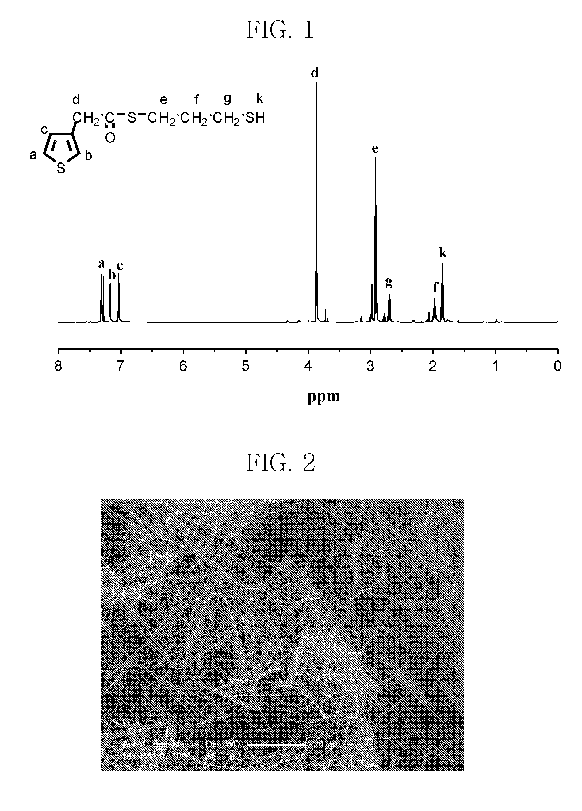
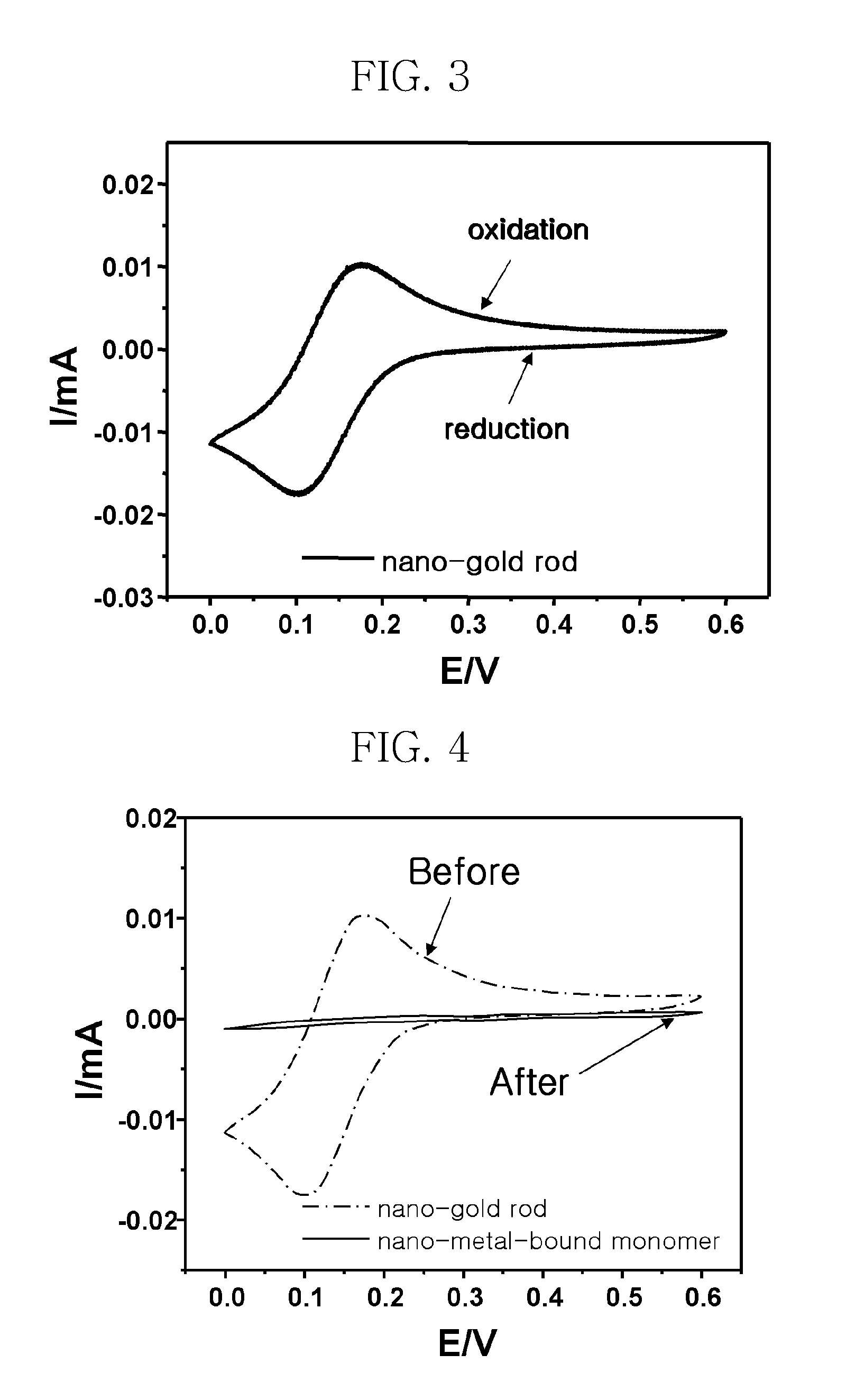
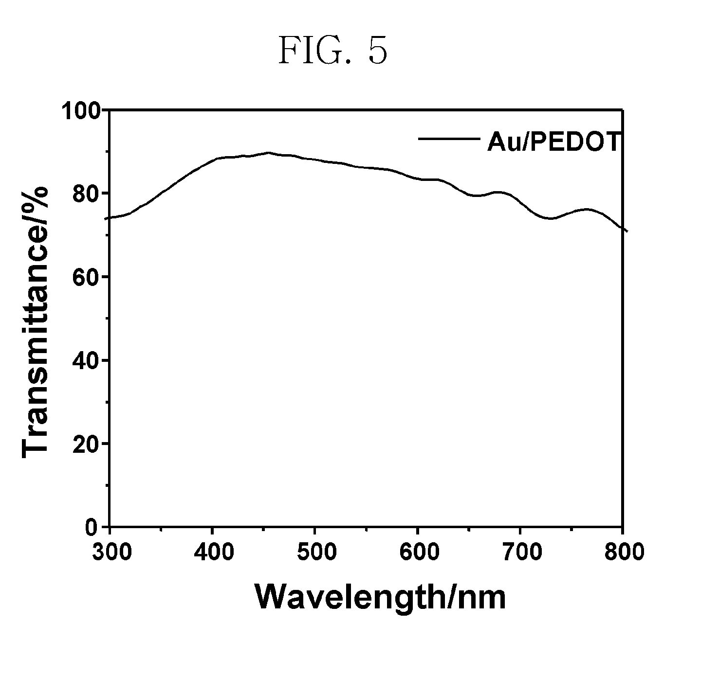
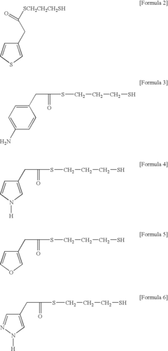
Monomer for binding nano-metal, conductive polymer composite and method of preparing the conductive polymer composite
PatentActiveUS20090286082A1
Innovation
- A monomer for binding nano-metal, represented by Formula 1, is used to create a conductive polymer composite with a nano-metal rod, where the monomer is attached to the nano-metal surface and then polymerized with a conductive polymer monomer and dopant, enhancing electrical conductivity and maintaining transparency and flexibility.
Electron conductive polymer composites and their use as electrode materials
PatentInactiveUS20200176762A1
Innovation
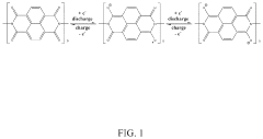
- A composite material is developed comprising an ion-permeable, non-electron conductive organic polymer core coated with an electron conductive polymer, specifically aromatic polyimide coated with conductive polythiophene (PI@PT), which enhances electronic conductivity and stability, enabling high reversible capacity and cycling stability in lithium-ion batteries.
Material Characterization Techniques
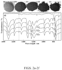
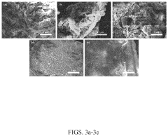
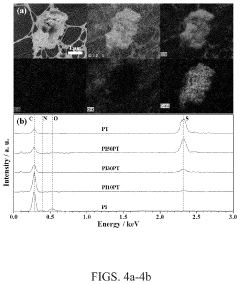
Material characterization techniques are essential for understanding the fundamental properties and performance of semiconductor-conductive polymer composites. Scanning Electron Microscopy (SEM) serves as a primary tool for visualizing the morphological features and dispersion quality of semiconductor particles within the polymer matrix. This technique provides critical insights into interface characteristics between components, which directly influence the composite's electrical conductivity pathways.
X-ray Diffraction (XRD) analysis enables researchers to identify crystalline phases and determine structural parameters of both the semiconductor fillers and polymer matrices. The crystallinity degree of polymers and the crystal structure of semiconductor particles can be precisely measured, offering valuable information about how these characteristics affect the overall conductivity mechanism of the composite.
Fourier Transform Infrared Spectroscopy (FTIR) plays a crucial role in identifying chemical interactions between semiconductor particles and polymer chains. By detecting shifts in characteristic absorption bands, FTIR can reveal the formation of chemical bonds or secondary interactions that may enhance or impede charge transfer at interfaces.
Thermal analysis techniques, including Differential Scanning Calorimetry (DSC) and Thermogravimetric Analysis (TGA), provide insights into the thermal stability and phase transitions of these composites. These properties are particularly important for applications requiring thermal reliability, as the glass transition temperature and decomposition behavior directly impact the operational temperature range of the final devices.
Electrical characterization methods form another critical category, encompassing four-point probe measurements for surface resistivity, impedance spectroscopy for frequency-dependent electrical response, and Hall effect measurements for carrier concentration and mobility determination. These techniques collectively provide a comprehensive understanding of charge transport mechanisms within the composite materials.
Advanced surface analysis techniques such as X-ray Photoelectron Spectroscopy (XPS) and Time-of-Flight Secondary Ion Mass Spectrometry (ToF-SIMS) offer detailed chemical composition information at surfaces and interfaces. These methods are particularly valuable for understanding the chemical environment at semiconductor-polymer interfaces where charge transfer occurs.
Atomic Force Microscopy (AFM) with conductive modes enables nanoscale mapping of electrical properties, allowing researchers to visualize conductive pathways and identify potential bottlenecks in charge transport. This technique bridges the gap between structural characterization and electrical performance, providing spatial resolution of conductivity variations across the composite.
Environmental Impact and Sustainability Considerations
The integration of semiconductors in conductive polymer composites presents significant environmental and sustainability considerations that must be addressed as this technology advances. The manufacturing processes for semiconductor materials typically involve energy-intensive procedures and the use of hazardous chemicals, including heavy metals and toxic solvents. These processes contribute to considerable carbon emissions and potential environmental contamination if not properly managed. Additionally, the extraction of rare earth elements and precious metals required for semiconductor production often leads to habitat destruction, soil degradation, and water pollution in mining regions.
Lifecycle assessment studies of semiconductor-enhanced polymer composites reveal complex environmental footprints. While these materials can enable more energy-efficient electronic devices and lighter components for transportation systems—potentially reducing operational environmental impacts—their production phase remains resource-intensive. The environmental cost-benefit analysis must therefore consider both manufacturing impacts and in-use benefits over the entire product lifecycle.
Recycling and end-of-life management present particular challenges for conductive polymer composites containing semiconductors. The intimate mixing of organic polymers with inorganic semiconductor materials creates complex waste streams that are difficult to separate using conventional recycling technologies. Current recycling rates for these advanced materials remain disappointingly low, with most end-of-life products being incinerated or landfilled, resulting in resource loss and potential environmental contamination.
Recent innovations in green chemistry approaches offer promising pathways toward more sustainable semiconductor-polymer composites. These include water-based processing methods, solvent-free polymerization techniques, and the development of biobased polymers that can interface effectively with semiconductor materials. Several research groups have demonstrated reduced-toxicity semiconductor dopants that maintain comparable conductivity while minimizing environmental hazards.
Regulatory frameworks worldwide are increasingly addressing the environmental aspects of electronic materials. The European Union's Restriction of Hazardous Substances (RoHS) directive and similar regulations in other regions have spurred innovation in developing semiconductor-polymer composites with reduced environmental impact. Industry leaders are responding by implementing closed-loop manufacturing systems and exploring alternative material formulations that maintain performance while reducing ecological footprints.
Looking forward, the sustainability of semiconductor-polymer composites will likely depend on circular economy approaches that design for disassembly and material recovery. Emerging technologies such as chemical depolymerization and selective solvent extraction show promise for separating valuable semiconductor components from polymer matrices at end-of-life. These developments, coupled with renewable energy adoption in manufacturing facilities, could significantly improve the overall environmental profile of these advanced materials.
Unlock deeper insights with Patsnap Eureka Quick Research — get a full tech report to explore trends and direct your research. Try now!
Generate Your Research Report Instantly with AI Agent
Supercharge your innovation with Patsnap Eureka AI Agent Platform!