

Exploring Material Usage in Resistive RAM Enhancements
OCT 9, 202510 MIN READ
Generate Your Research Report Instantly with AI Agent
PatSnap Eureka helps you evaluate technical feasibility & market potential.
RRAM Material Evolution and Research Objectives
Resistive Random Access Memory (RRAM) has emerged as a promising candidate for next-generation non-volatile memory technologies due to its simple structure, high density, low power consumption, and compatibility with CMOS processes. The evolution of RRAM materials represents a critical aspect of its development trajectory, with significant advancements occurring over the past two decades.
Initially, binary metal oxides such as TiO2, HfO2, and Ta2O5 dominated early RRAM research due to their simplicity and compatibility with existing semiconductor manufacturing processes. These materials demonstrated the fundamental resistive switching phenomenon but suffered from reliability issues and performance limitations. The first-generation devices typically exhibited high operating voltages, limited endurance, and inconsistent switching behavior.
As research progressed, complex oxides including perovskites (SrTiO3, BiFeO3) and spinel structures gained attention for their unique electronic properties and enhanced switching characteristics. These materials offered improved control over oxygen vacancy migration, which is fundamental to the resistive switching mechanism in oxide-based RRAM. Concurrently, the introduction of bilayer and multilayer oxide structures enabled better control over the switching process by engineering the interface properties.
A significant breakthrough came with the exploration of two-dimensional (2D) materials such as graphene, MoS2, and h-BN as active layers or electrodes in RRAM devices. These materials provided atomically thin barriers with unique electronic properties, potentially enabling ultra-scaled memory cells with reduced variability. The incorporation of 2D materials has opened new avenues for flexible and transparent memory applications.
Recent research has focused on chalcogenide-based materials, particularly phase-change materials and solid electrolytes for conductive-bridge RAM (CBRAM), offering alternative switching mechanisms with potential advantages in switching speed and power consumption. Additionally, organic and polymer-based RRAM has gained traction for applications requiring flexibility, biocompatibility, and low-cost manufacturing.
The primary research objectives in RRAM material development currently include enhancing retention time and endurance, reducing operating voltages, improving switching uniformity, and addressing scalability challenges. Material engineering approaches aim to optimize the trade-off between these parameters while maintaining CMOS compatibility.
Future research directions point toward hybrid material systems that combine the advantages of different material classes, atomic-level interface engineering, and the incorporation of novel dopants to control defect formation and migration. Additionally, there is growing interest in neuromorphic applications, where material properties can be tailored to mimic synaptic behavior for brain-inspired computing architectures.
The ultimate goal remains the development of RRAM materials that can simultaneously achieve high performance, reliability, and manufacturability to enable commercial adoption in various applications ranging from storage-class memory to embedded systems and neuromorphic computing platforms.
Initially, binary metal oxides such as TiO2, HfO2, and Ta2O5 dominated early RRAM research due to their simplicity and compatibility with existing semiconductor manufacturing processes. These materials demonstrated the fundamental resistive switching phenomenon but suffered from reliability issues and performance limitations. The first-generation devices typically exhibited high operating voltages, limited endurance, and inconsistent switching behavior.
As research progressed, complex oxides including perovskites (SrTiO3, BiFeO3) and spinel structures gained attention for their unique electronic properties and enhanced switching characteristics. These materials offered improved control over oxygen vacancy migration, which is fundamental to the resistive switching mechanism in oxide-based RRAM. Concurrently, the introduction of bilayer and multilayer oxide structures enabled better control over the switching process by engineering the interface properties.
A significant breakthrough came with the exploration of two-dimensional (2D) materials such as graphene, MoS2, and h-BN as active layers or electrodes in RRAM devices. These materials provided atomically thin barriers with unique electronic properties, potentially enabling ultra-scaled memory cells with reduced variability. The incorporation of 2D materials has opened new avenues for flexible and transparent memory applications.
Recent research has focused on chalcogenide-based materials, particularly phase-change materials and solid electrolytes for conductive-bridge RAM (CBRAM), offering alternative switching mechanisms with potential advantages in switching speed and power consumption. Additionally, organic and polymer-based RRAM has gained traction for applications requiring flexibility, biocompatibility, and low-cost manufacturing.
The primary research objectives in RRAM material development currently include enhancing retention time and endurance, reducing operating voltages, improving switching uniformity, and addressing scalability challenges. Material engineering approaches aim to optimize the trade-off between these parameters while maintaining CMOS compatibility.
Future research directions point toward hybrid material systems that combine the advantages of different material classes, atomic-level interface engineering, and the incorporation of novel dopants to control defect formation and migration. Additionally, there is growing interest in neuromorphic applications, where material properties can be tailored to mimic synaptic behavior for brain-inspired computing architectures.
The ultimate goal remains the development of RRAM materials that can simultaneously achieve high performance, reliability, and manufacturability to enable commercial adoption in various applications ranging from storage-class memory to embedded systems and neuromorphic computing platforms.
Market Analysis for Next-Generation Memory Solutions
The global next-generation memory market is experiencing robust growth, driven by increasing demand for faster, more energy-efficient, and higher-density memory solutions. The resistive RAM (ReRAM) segment specifically is projected to grow at a compound annual growth rate of 16% through 2028, with the overall emerging memory technologies market expected to reach $20 billion by 2030. This growth is primarily fueled by expanding applications in data centers, artificial intelligence systems, and edge computing devices.
Consumer electronics remains the largest application sector for next-generation memory technologies, accounting for approximately 40% of the market share. However, enterprise storage systems and automotive applications are rapidly emerging as significant growth segments, with the latter expected to see the highest growth rate over the next five years due to increasing electronic content in vehicles and the rise of autonomous driving systems.
Material innovation in ReRAM technology is creating substantial market opportunities. The shift from traditional metal oxide materials to advanced composites and 2D materials is enabling performance improvements that address key market requirements. Devices utilizing hafnium oxide-based ReRAM have demonstrated 30% better switching speeds compared to conventional alternatives, creating premium market segments for high-performance computing applications.
Regional analysis reveals that Asia-Pacific dominates the manufacturing landscape with 65% of production capacity, while North America leads in research and development investment. Europe is gaining ground through focused initiatives in automotive and industrial applications of ReRAM technologies. This geographic distribution is reshaping supply chains and influencing strategic partnerships across the memory ecosystem.
Market adoption barriers include cost considerations, with ReRAM solutions currently commanding a 2-3x price premium over conventional DRAM and NAND flash memory. However, this gap is narrowing as manufacturing processes mature and economies of scale improve. Industry analysts predict price parity with traditional memory technologies could be achieved within 4-6 years for specific application segments.
Customer requirements are increasingly diverging between consumer and enterprise markets. While consumer applications prioritize cost efficiency and form factor, enterprise customers emphasize reliability, endurance, and total cost of ownership. This market segmentation is driving specialized material development pathways in ReRAM technology, with different material compositions being optimized for specific market verticals.
The competitive landscape features both established memory manufacturers pivoting toward ReRAM and specialized startups focusing exclusively on novel material implementations. Strategic partnerships between material suppliers, device manufacturers, and system integrators are becoming essential for market success, creating a complex ecosystem of interdependent stakeholders.
Consumer electronics remains the largest application sector for next-generation memory technologies, accounting for approximately 40% of the market share. However, enterprise storage systems and automotive applications are rapidly emerging as significant growth segments, with the latter expected to see the highest growth rate over the next five years due to increasing electronic content in vehicles and the rise of autonomous driving systems.
Material innovation in ReRAM technology is creating substantial market opportunities. The shift from traditional metal oxide materials to advanced composites and 2D materials is enabling performance improvements that address key market requirements. Devices utilizing hafnium oxide-based ReRAM have demonstrated 30% better switching speeds compared to conventional alternatives, creating premium market segments for high-performance computing applications.
Regional analysis reveals that Asia-Pacific dominates the manufacturing landscape with 65% of production capacity, while North America leads in research and development investment. Europe is gaining ground through focused initiatives in automotive and industrial applications of ReRAM technologies. This geographic distribution is reshaping supply chains and influencing strategic partnerships across the memory ecosystem.
Market adoption barriers include cost considerations, with ReRAM solutions currently commanding a 2-3x price premium over conventional DRAM and NAND flash memory. However, this gap is narrowing as manufacturing processes mature and economies of scale improve. Industry analysts predict price parity with traditional memory technologies could be achieved within 4-6 years for specific application segments.
Customer requirements are increasingly diverging between consumer and enterprise markets. While consumer applications prioritize cost efficiency and form factor, enterprise customers emphasize reliability, endurance, and total cost of ownership. This market segmentation is driving specialized material development pathways in ReRAM technology, with different material compositions being optimized for specific market verticals.
The competitive landscape features both established memory manufacturers pivoting toward ReRAM and specialized startups focusing exclusively on novel material implementations. Strategic partnerships between material suppliers, device manufacturers, and system integrators are becoming essential for market success, creating a complex ecosystem of interdependent stakeholders.
Current RRAM Material Limitations and Technical Barriers
Despite significant advancements in RRAM technology, several material-related limitations and technical barriers continue to impede its widespread commercial adoption. The primary challenge lies in the inherent variability of switching behavior in RRAM devices, which stems from the stochastic nature of filament formation and rupture processes. This variability manifests as inconsistent resistance states, unpredictable switching voltages, and fluctuating retention times across devices, even within the same manufacturing batch.
Metal oxide materials, while popular for RRAM applications, exhibit significant limitations. Titanium oxide (TiO2) and hafnium oxide (HfO2) demonstrate excellent endurance but suffer from oxygen vacancy migration issues that lead to degradation over repeated cycling. Tantalum oxide (Ta2O5) offers improved stability but requires higher operating voltages, increasing power consumption and limiting integration density.
Interface engineering presents another critical barrier. The electrode-oxide interface quality significantly impacts device performance, with non-uniform interfaces leading to inconsistent switching characteristics. Current deposition techniques struggle to achieve atomically smooth interfaces at scale, resulting in performance variations across large memory arrays.
Scaling challenges represent a substantial technical hurdle for RRAM commercialization. As device dimensions shrink below 20nm, quantum effects and thermal instabilities become increasingly pronounced, affecting filament stability and retention characteristics. The confined geometry at nanoscale dimensions exacerbates material defects and interface irregularities, further compromising reliability.
The multi-level cell (MLC) capability, essential for high-density storage applications, faces significant material constraints. Current materials exhibit insufficient resistance state separation and stability to reliably support more than 2-3 distinct levels, limiting storage density potential. The resistance drift phenomenon, particularly pronounced in chalcogenide-based RRAM, undermines long-term data retention in MLC implementations.
Manufacturing integration poses additional challenges. Many promising RRAM materials require processing conditions incompatible with standard CMOS fabrication flows. High-temperature annealing steps necessary for optimal oxide formation often conflict with thermal budgets of advanced logic processes. Additionally, materials like copper and silver used in conductive-bridge RRAMs present contamination risks to CMOS transistors.
Reliability under extreme conditions remains problematic. Temperature sensitivity affects both data retention and switching characteristics, with many materials showing significant performance degradation outside narrow temperature ranges. Radiation hardness, critical for aerospace and military applications, varies widely among RRAM materials, with few options demonstrating sufficient resilience against high-energy particle impacts.
Metal oxide materials, while popular for RRAM applications, exhibit significant limitations. Titanium oxide (TiO2) and hafnium oxide (HfO2) demonstrate excellent endurance but suffer from oxygen vacancy migration issues that lead to degradation over repeated cycling. Tantalum oxide (Ta2O5) offers improved stability but requires higher operating voltages, increasing power consumption and limiting integration density.
Interface engineering presents another critical barrier. The electrode-oxide interface quality significantly impacts device performance, with non-uniform interfaces leading to inconsistent switching characteristics. Current deposition techniques struggle to achieve atomically smooth interfaces at scale, resulting in performance variations across large memory arrays.
Scaling challenges represent a substantial technical hurdle for RRAM commercialization. As device dimensions shrink below 20nm, quantum effects and thermal instabilities become increasingly pronounced, affecting filament stability and retention characteristics. The confined geometry at nanoscale dimensions exacerbates material defects and interface irregularities, further compromising reliability.
The multi-level cell (MLC) capability, essential for high-density storage applications, faces significant material constraints. Current materials exhibit insufficient resistance state separation and stability to reliably support more than 2-3 distinct levels, limiting storage density potential. The resistance drift phenomenon, particularly pronounced in chalcogenide-based RRAM, undermines long-term data retention in MLC implementations.
Manufacturing integration poses additional challenges. Many promising RRAM materials require processing conditions incompatible with standard CMOS fabrication flows. High-temperature annealing steps necessary for optimal oxide formation often conflict with thermal budgets of advanced logic processes. Additionally, materials like copper and silver used in conductive-bridge RRAMs present contamination risks to CMOS transistors.
Reliability under extreme conditions remains problematic. Temperature sensitivity affects both data retention and switching characteristics, with many materials showing significant performance degradation outside narrow temperature ranges. Radiation hardness, critical for aerospace and military applications, varies widely among RRAM materials, with few options demonstrating sufficient resilience against high-energy particle impacts.
State-of-the-Art Material Solutions for RRAM Devices
01 Metal oxide materials for RRAM
Metal oxides are widely used as switching materials in RRAM devices due to their excellent resistive switching properties. These materials include hafnium oxide (HfO2), titanium oxide (TiO2), tantalum oxide (Ta2O5), and zirconium oxide (ZrO2). The oxygen vacancy movement within these metal oxides facilitates the formation and rupture of conductive filaments, enabling the switching between high and low resistance states. These materials offer advantages such as good compatibility with CMOS processes, high endurance, and reliable data retention.- Metal oxide materials for RRAM: Metal oxides are widely used as switching materials in RRAM devices due to their excellent resistive switching properties. These materials include hafnium oxide (HfO2), titanium oxide (TiO2), tantalum oxide (Ta2O5), and zirconium oxide (ZrO2). The oxygen vacancy movement in these metal oxides enables the formation and rupture of conductive filaments, which is the fundamental mechanism for resistive switching in RRAM. These materials offer advantages such as high on/off ratio, good endurance, and compatibility with CMOS fabrication processes.
- Two-dimensional materials for RRAM: Two-dimensional (2D) materials have emerged as promising candidates for RRAM applications due to their unique properties such as atomic thickness, tunable bandgap, and mechanical flexibility. Materials like graphene, transition metal dichalcogenides (TMDs), and hexagonal boron nitride (h-BN) are being explored for RRAM devices. These 2D materials can serve as electrodes, switching layers, or barrier layers in RRAM structures, offering advantages such as reduced power consumption, improved switching speed, and enhanced device scalability.
- Chalcogenide materials for RRAM: Chalcogenide materials, particularly those containing sulfur, selenium, or tellurium, are extensively used in RRAM devices. These materials, including germanium selenide (GeSe), copper telluride (CuTe), and various metal sulfides, exhibit phase-change properties that enable resistive switching. The formation of metal-chalcogenide complexes or the migration of metal ions through a chalcogenide solid electrolyte creates conductive pathways that can be controlled electrically. These materials offer advantages such as multi-level storage capability, good retention, and relatively low operating voltages.
- Polymer and organic materials for RRAM: Polymer and organic materials are being investigated for flexible and biocompatible RRAM applications. These materials include conductive polymers like PEDOT:PSS, polyaniline, and various organic semiconductors. The resistive switching in these materials typically occurs through mechanisms such as charge trapping/detrapping, conformational changes, or redox processes. Polymer-based RRAM offers advantages including mechanical flexibility, solution processability, low-cost fabrication, and potential biodegradability, making them suitable for wearable electronics and biomedical applications.
- Composite and multilayer materials for RRAM: Composite and multilayer material structures are designed to enhance RRAM performance by combining the advantages of different materials. These structures include metal oxide/polymer composites, oxide/nitride stacks, and metal nanoparticle-embedded dielectrics. The interfaces between different materials play a crucial role in the resistive switching behavior. By engineering these interfaces and creating multilayer structures, parameters such as switching voltage, endurance, retention time, and uniformity can be optimized. These composite structures also enable the implementation of specialized functions like selector devices for crossbar arrays.
02 Two-dimensional materials for RRAM
Two-dimensional (2D) materials are emerging as promising candidates for RRAM applications due to their unique electronic properties and atomic-scale thickness. Materials such as graphene, transition metal dichalcogenides (TMDs), and hexagonal boron nitride (h-BN) are being explored for resistive switching applications. These 2D materials offer advantages including flexibility, transparency, and the potential for scaling to ultra-small dimensions. The controlled defect engineering in these materials allows for tunable resistive switching behavior and improved device performance.Expand Specific Solutions03 Chalcogenide materials for RRAM
Chalcogenide materials, particularly phase-change materials containing elements such as germanium, antimony, and tellurium (GST), are utilized in RRAM devices. These materials can switch between amorphous and crystalline phases with different resistivity values. The phase transition can be induced by electrical pulses, enabling resistive switching behavior. Chalcogenide-based RRAM offers advantages such as multi-level storage capability, fast switching speed, and good retention characteristics, making them suitable for non-volatile memory applications.Expand Specific Solutions04 Perovskite materials for RRAM
Perovskite materials with the general formula ABO3 are being investigated for RRAM applications due to their unique electronic and ionic transport properties. Materials such as strontium titanate (SrTiO3), barium titanate (BaTiO3), and lanthanum manganite (LaMnO3) exhibit resistive switching behavior through the migration of oxygen vacancies or metal cations. These materials offer advantages including high ON/OFF ratios, good endurance, and the ability to tune their properties through doping and composition engineering.Expand Specific Solutions05 Multilayer and composite materials for RRAM
Multilayer and composite material structures are designed to enhance RRAM performance by combining the advantages of different materials. These structures typically consist of multiple layers of different materials, such as metal/oxide/metal stacks or oxide/oxide heterojunctions. The interfaces between different materials play a crucial role in the resistive switching mechanism. By engineering these multilayer structures, parameters such as switching voltage, endurance, retention, and uniformity can be optimized. Additionally, the incorporation of nanoparticles or dopants into the switching layer can further enhance device performance.Expand Specific Solutions
Leading Companies and Research Institutions in RRAM Technology
The Resistive RAM (ReRAM) technology landscape is currently in a growth phase, with the market expected to reach significant expansion as memory demands increase across IoT, AI, and data center applications. The technology demonstrates moderate maturity, with major players like Samsung Electronics, IBM, and Micron Technology driving commercial development while academic institutions such as Peking University and Fudan University contribute fundamental research. Companies including KIOXIA, SK hynix, and TetraMem are advancing specialized implementations, while semiconductor manufacturers like TSMC, SMIC, and UMC provide essential fabrication capabilities. The competitive landscape features both established memory giants and innovative startups like Innostar Semiconductor, creating a dynamic environment where material innovation remains a critical differentiator for next-generation ReRAM solutions.
Samsung Electronics Co., Ltd.
Technical Solution: Samsung has pioneered advanced material engineering for ReRAM technology through their development of filamentary switching mechanisms using transition metal oxides (TMOs). Their approach focuses on hafnium oxide (HfOx) and tantalum oxide (TaOx) bilayer structures that create controlled oxygen vacancy filaments for reliable resistive switching[1]. Samsung's proprietary "atom switch" technology incorporates noble metals (Ag, Cu) as active electrodes with solid electrolytes to form and dissolve conductive bridges during operation[2]. They've also developed innovative doping strategies, introducing elements like aluminum into HfOx to stabilize the switching behavior and reduce variability between cycles[3]. Samsung's 3D vertical ReRAM architecture enables high-density integration while maintaining performance, achieving sub-10nm feature sizes with specialized atomic layer deposition techniques that ensure uniform material properties throughout the memory array[4].
Strengths: Samsung's material engineering expertise allows for excellent scalability down to advanced nodes while maintaining performance metrics. Their multi-layer oxide approach provides better control over switching behavior and reliability. Weaknesses: Their complex material stacks require sophisticated manufacturing processes that may impact yield and cost-effectiveness compared to simpler ReRAM implementations.
KIOXIA Corp.
Technical Solution: KIOXIA (formerly Toshiba Memory) has developed a distinctive ReRAM technology based on their proprietary metal oxide materials engineering. Their approach centers on tantalum oxide (TaOx) as the primary switching medium, with carefully controlled oxygen stoichiometry to create a dual-layer structure consisting of oxygen-rich (TaO2) and oxygen-deficient (TaO) regions[1]. This engineered oxygen gradient facilitates controlled filament formation and dissolution. KIOXIA's material innovation includes the integration of a "scavenging layer" made of titanium or hafnium adjacent to the switching oxide, which regulates oxygen ion distribution during operation and enhances switching uniformity[2]. They've pioneered specialized atomic layer deposition techniques that enable precise control of layer thicknesses down to sub-nanometer scales while maintaining excellent conformality for 3D integration[3]. KIOXIA has also developed unique electrode materials including ruthenium oxide (RuO2) that serve as both excellent conductors and oxygen reservoirs, contributing to the overall stability of their ReRAM cells during repeated cycling[4].
Strengths: KIOXIA's material technology enables excellent scalability below 20nm feature sizes while maintaining performance metrics. Their engineered oxygen gradients provide superior control over switching behavior and reliability. Weaknesses: The complex material stack requires sophisticated deposition and etching processes that may impact manufacturing throughput and cost-effectiveness compared to simpler memory technologies.
Critical Patents and Breakthroughs in RRAM Material Science
Resistive random access memory and fabrication method thereof
PatentActiveEP3151295A3
Innovation
- A fabrication method involving a substrate with a bottom electrode, a resistance switching layer made of amorphous silicon, and a barrier layer of silicon oxide or silicon nitride, formed using plasma-enhanced vapor deposition, to prevent atom diffusion and enhance the structural integrity and conductivity of the top electrode.


Resistive random access memory with high uniformity and low power consumption and method for fabricating the same
PatentInactiveUS20160225987A1
Innovation
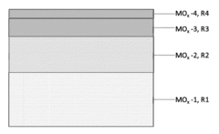
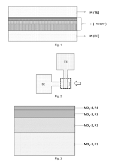
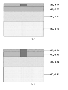
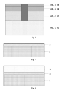
- A four-layer resistive material film structure with increasing oxygen concentrations and decreasing thicknesses is used, allowing for controlled formation and rupture of conductive filaments, enabling 2-bit storage with high uniformity and low power consumption, and potentially achieving 3-bit or higher density storage by adjusting resistance values in each layer.
Manufacturing Scalability and Integration Challenges
The scalability of Resistive RAM (ReRAM) manufacturing processes represents a critical challenge in transitioning this promising technology from laboratory demonstrations to commercial production. Current fabrication techniques face significant hurdles when attempting to maintain consistent switching characteristics across large arrays of memory cells. The variability in resistance states between cells manufactured using identical processes can exceed 20%, creating reliability concerns for high-density memory applications. This cell-to-cell variation stems primarily from difficulties in precisely controlling material deposition thickness and composition at nanometer scales.
Integration with existing CMOS technology presents another substantial challenge. While ReRAM offers potential for back-end-of-line (BEOL) integration, the thermal budget constraints of CMOS processes (typically limited to 400-450°C) restrict material choices and annealing procedures. Many promising ReRAM materials require higher temperature processing to achieve optimal electrical characteristics, creating a fundamental compatibility issue. Additionally, the etching processes used for patterning ReRAM materials can introduce damage to the switching layer, further compromising device performance.
The selection of electrode materials significantly impacts both manufacturing yield and long-term reliability. Noble metals like platinum and gold demonstrate excellent electrical properties but present cost and integration challenges at scale. Alternative electrode materials such as TiN, TaN, and doped silicon show promise but may introduce additional interface reactions that affect switching behavior. The electrode-oxide interface quality proves particularly critical, as defects at this boundary can dramatically alter the formation and rupture of conductive filaments.
Scaling ReRAM cells below 20nm introduces quantum effects that can destabilize the conductive filament formation process. At these dimensions, the statistical nature of ion migration becomes more pronounced, leading to greater variability in switching voltages and resistance states. Furthermore, the reduced number of atoms participating in filament formation at smaller scales increases susceptibility to random telegraph noise and other quantum fluctuations, potentially limiting the practical scaling limits of certain ReRAM material systems.
The development of specialized deposition techniques represents a promising approach to addressing these challenges. Atomic Layer Deposition (ALD) offers precise control over film thickness and composition but typically operates at slower deposition rates than methods like sputtering. Recent innovations in plasma-enhanced ALD show potential for maintaining material quality while improving throughput. Similarly, advances in reactive sputtering with in-situ monitoring capabilities are enabling better control of oxygen stoichiometry in metal oxide ReRAM materials, a critical factor in device performance.
Integration with existing CMOS technology presents another substantial challenge. While ReRAM offers potential for back-end-of-line (BEOL) integration, the thermal budget constraints of CMOS processes (typically limited to 400-450°C) restrict material choices and annealing procedures. Many promising ReRAM materials require higher temperature processing to achieve optimal electrical characteristics, creating a fundamental compatibility issue. Additionally, the etching processes used for patterning ReRAM materials can introduce damage to the switching layer, further compromising device performance.
The selection of electrode materials significantly impacts both manufacturing yield and long-term reliability. Noble metals like platinum and gold demonstrate excellent electrical properties but present cost and integration challenges at scale. Alternative electrode materials such as TiN, TaN, and doped silicon show promise but may introduce additional interface reactions that affect switching behavior. The electrode-oxide interface quality proves particularly critical, as defects at this boundary can dramatically alter the formation and rupture of conductive filaments.
Scaling ReRAM cells below 20nm introduces quantum effects that can destabilize the conductive filament formation process. At these dimensions, the statistical nature of ion migration becomes more pronounced, leading to greater variability in switching voltages and resistance states. Furthermore, the reduced number of atoms participating in filament formation at smaller scales increases susceptibility to random telegraph noise and other quantum fluctuations, potentially limiting the practical scaling limits of certain ReRAM material systems.
The development of specialized deposition techniques represents a promising approach to addressing these challenges. Atomic Layer Deposition (ALD) offers precise control over film thickness and composition but typically operates at slower deposition rates than methods like sputtering. Recent innovations in plasma-enhanced ALD show potential for maintaining material quality while improving throughput. Similarly, advances in reactive sputtering with in-situ monitoring capabilities are enabling better control of oxygen stoichiometry in metal oxide ReRAM materials, a critical factor in device performance.
Environmental Impact and Sustainability of RRAM Materials
The environmental footprint of Resistive RAM (RRAM) materials represents a critical consideration in the sustainable development of next-generation memory technologies. Current RRAM devices predominantly utilize transition metal oxides such as HfO2, TiO2, and Ta2O5, which present varying degrees of environmental concerns throughout their lifecycle. The extraction processes for these materials often involve energy-intensive mining operations that contribute to habitat destruction, water pollution, and significant carbon emissions. Particularly, rare earth elements sometimes incorporated in RRAM structures pose severe environmental challenges due to their extraction methods that frequently employ toxic chemicals and generate radioactive waste.
Manufacturing processes for RRAM devices require high-purity materials and precise deposition techniques that consume substantial energy and utilize potentially harmful chemicals including strong acids and organic solvents. The semiconductor industry's traditional reliance on perfluorinated compounds (PFCs) with high global warming potential further compounds these environmental concerns. Water usage in fabrication facilities also remains a significant sustainability challenge, with a single manufacturing plant potentially consuming millions of gallons daily.
End-of-life considerations for RRAM technologies present additional environmental challenges. The complex material composition of these devices complicates recycling efforts, with precious metals and rare earth elements often lost during disposal. E-waste containing these materials can leach toxic substances into soil and groundwater when improperly managed, creating long-term environmental hazards.
Encouragingly, several sustainability initiatives are emerging within the RRAM development community. Research into bio-compatible and biodegradable materials for RRAM structures represents a promising direction, with organic materials and naturally derived compounds showing potential as switching layers. Silicon-based alternatives to rare earth elements are being explored to reduce dependence on environmentally problematic materials.
Energy efficiency improvements in RRAM manufacturing are being pursued through optimized deposition techniques and lower-temperature processes. Additionally, design-for-recycling approaches are gaining traction, with modular architectures that facilitate material recovery and reuse. Several leading semiconductor manufacturers have established ambitious sustainability targets, including commitments to carbon neutrality, water conservation, and zero-waste operations by 2030.
The path toward truly sustainable RRAM technologies requires holistic lifecycle assessment methodologies that account for environmental impacts from raw material extraction through manufacturing, use, and eventual disposal. Regulatory frameworks worldwide are increasingly mandating such comprehensive environmental impact evaluations, driving the industry toward greener material choices and manufacturing processes.
Manufacturing processes for RRAM devices require high-purity materials and precise deposition techniques that consume substantial energy and utilize potentially harmful chemicals including strong acids and organic solvents. The semiconductor industry's traditional reliance on perfluorinated compounds (PFCs) with high global warming potential further compounds these environmental concerns. Water usage in fabrication facilities also remains a significant sustainability challenge, with a single manufacturing plant potentially consuming millions of gallons daily.
End-of-life considerations for RRAM technologies present additional environmental challenges. The complex material composition of these devices complicates recycling efforts, with precious metals and rare earth elements often lost during disposal. E-waste containing these materials can leach toxic substances into soil and groundwater when improperly managed, creating long-term environmental hazards.
Encouragingly, several sustainability initiatives are emerging within the RRAM development community. Research into bio-compatible and biodegradable materials for RRAM structures represents a promising direction, with organic materials and naturally derived compounds showing potential as switching layers. Silicon-based alternatives to rare earth elements are being explored to reduce dependence on environmentally problematic materials.
Energy efficiency improvements in RRAM manufacturing are being pursued through optimized deposition techniques and lower-temperature processes. Additionally, design-for-recycling approaches are gaining traction, with modular architectures that facilitate material recovery and reuse. Several leading semiconductor manufacturers have established ambitious sustainability targets, including commitments to carbon neutrality, water conservation, and zero-waste operations by 2030.
The path toward truly sustainable RRAM technologies requires holistic lifecycle assessment methodologies that account for environmental impacts from raw material extraction through manufacturing, use, and eventual disposal. Regulatory frameworks worldwide are increasingly mandating such comprehensive environmental impact evaluations, driving the industry toward greener material choices and manufacturing processes.
Unlock deeper insights with PatSnap Eureka Quick Research — get a full tech report to explore trends and direct your research. Try now!
Generate Your Research Report Instantly with AI Agent
Supercharge your innovation with PatSnap Eureka AI Agent Platform!