Exploring Spray Pyrolysis Efficacy in Semiconductor Manufacturing
SEP 25, 20259 MIN READ
Generate Your Research Report Instantly with AI Agent
PatSnap Eureka helps you evaluate technical feasibility & market potential.
Spray Pyrolysis Evolution and Objectives
Spray pyrolysis has evolved significantly since its inception in the 1960s as a simple solution-based deposition technique. Initially developed for oxide thin film production, this versatile method has transformed through decades of refinement to become increasingly relevant in semiconductor manufacturing. The evolution trajectory shows a clear progression from basic manual setups to sophisticated automated systems capable of precise control over film properties at the nanoscale.
The fundamental principle of spray pyrolysis—atomizing precursor solutions onto heated substrates to form solid films through thermal decomposition—has remained consistent, while innovations in delivery systems, precursor chemistry, and process control have dramatically expanded its capabilities. Early applications were limited to simple oxide coatings, but technological advancements have enabled the deposition of complex multi-component materials with tailored electrical, optical, and structural properties essential for modern semiconductor devices.
A significant evolutionary milestone occurred in the 1990s with the integration of computer-controlled parameters, allowing for reproducible thin film characteristics. The 2000s witnessed further refinement with the development of ultrasonic and pressure-assisted atomization techniques, substantially improving film uniformity and reducing defect density—critical factors for semiconductor applications. Recent innovations include the implementation of multi-zone heating systems and in-situ monitoring capabilities, enabling real-time adjustments during the deposition process.
The primary objective of exploring spray pyrolysis efficacy in semiconductor manufacturing is to establish this technique as a cost-effective alternative to conventional vacuum-based deposition methods while maintaining comparable film quality. Specific technical goals include achieving sub-10nm thickness control, enhancing compositional uniformity across large substrates (>300mm), and developing processes compatible with temperature-sensitive substrates for flexible electronics applications.
Additional objectives encompass the optimization of precursor chemistries to minimize contamination levels below industry-standard thresholds, particularly for critical dopants and trace elements that significantly impact semiconductor performance. The research also aims to develop scalable processes suitable for high-volume manufacturing environments, with throughput rates competitive with established techniques like chemical vapor deposition and sputtering.
Long-term technical goals include establishing spray pyrolysis as a viable method for advanced semiconductor materials, including high-k dielectrics, transparent conducting oxides, and compound semiconductors for next-generation devices. The ultimate objective is to position spray pyrolysis as a sustainable manufacturing technique with reduced environmental impact through lower energy consumption and decreased use of toxic precursors compared to conventional methods.
Semiconductor Market Demand Analysis
The semiconductor industry has witnessed unprecedented growth in recent years, with the global market value reaching $555.9 billion in 2021 and projections indicating further expansion to approximately $1 trillion by 2030. This remarkable growth trajectory is primarily driven by increasing digitalization across industries, the proliferation of smart devices, and emerging technologies such as artificial intelligence, Internet of Things (IoT), and autonomous vehicles.
Spray pyrolysis technology addresses several critical market demands within semiconductor manufacturing. The miniaturization trend continues unabated, with leading manufacturers pushing toward 3nm and 2nm process nodes. This miniaturization necessitates more precise deposition techniques for thin films, where spray pyrolysis offers significant advantages due to its ability to create uniform, high-quality thin films at relatively lower costs compared to conventional methods.
The demand for more energy-efficient semiconductor manufacturing processes has become paramount as sustainability concerns grow. Market research indicates that approximately 70% of semiconductor companies have established carbon reduction targets. Spray pyrolysis potentially offers reduced energy consumption compared to vacuum-based deposition methods, aligning with this industry-wide sustainability push.
Cost considerations remain a dominant factor in semiconductor manufacturing decisions. The semiconductor equipment market alone was valued at $95.9 billion in 2021, with thin film deposition equipment comprising a significant portion. Spray pyrolysis presents an economically viable alternative to expensive vacuum-based techniques, potentially reducing capital expenditure by 30-40% for certain applications.
Emerging applications in flexible electronics, photovoltaics, and sensors are creating new market segments where conventional semiconductor manufacturing techniques face limitations. The global flexible electronics market is growing at a CAGR of 11.2%, reaching $42.2 billion by 2027. Spray pyrolysis's ability to deposit films on various substrates, including flexible materials, positions it favorably within these growing market segments.
Regional analysis reveals shifting dynamics in semiconductor manufacturing. While East Asia continues to dominate with approximately 60% of global semiconductor manufacturing capacity, significant investments are being made in the United States and Europe to reduce dependency on Asian supply chains. This regionalization trend creates opportunities for implementing newer technologies like spray pyrolysis in newly established facilities.
The automotive semiconductor market deserves special attention, with projections indicating growth from $43.6 billion in 2021 to $78.5 billion by 2026. The transition to electric vehicles and advanced driver-assistance systems is driving demand for specialized semiconductor components where spray pyrolysis could offer advantages in manufacturing certain sensor elements and power electronics components.
Current Spray Pyrolysis Challenges
Spray pyrolysis technology in semiconductor manufacturing faces several significant challenges that limit its widespread industrial adoption despite its promising attributes. The primary obstacle remains achieving uniform thin film deposition across large substrate areas. Current spray systems struggle to maintain consistent droplet size distribution and velocity, resulting in thickness variations that can exceed acceptable tolerances for high-performance semiconductor devices. This non-uniformity becomes particularly problematic as wafer sizes increase to meet industry demands for higher throughput and cost reduction.
Material utilization efficiency presents another major challenge, with conventional spray pyrolysis systems typically achieving only 15-30% precursor utilization rates. The remainder becomes waste, raising both environmental concerns and increasing production costs. This inefficiency stems from overspray, solution drainage, and precursor decomposition before reaching the target substrate. For high-value semiconductor materials containing rare or precious metals, this waste significantly impacts economic viability.
Temperature control during the deposition process remains critically challenging. The rapid evaporation of solvents during spraying creates localized cooling effects that can disrupt the thermal profile across the substrate. These thermal gradients lead to inconsistent crystallization, defect formation, and compromised electrical properties in the resulting films. Current heating systems struggle to compensate for these dynamic thermal fluctuations in real-time.
Precursor chemistry optimization represents another substantial hurdle. Finding stable precursor solutions that decompose cleanly at moderate temperatures while yielding high-purity semiconductor materials proves difficult. Many conventional precursors either decompose prematurely or leave carbon and other contaminants in the films, degrading device performance. The development of novel precursor chemistries specifically tailored for spray pyrolysis remains underdeveloped compared to other deposition techniques.
Integration challenges with existing semiconductor manufacturing workflows further complicate adoption. Spray pyrolysis equipment typically requires significant floor space and specialized ventilation systems to handle solvent vapors and byproducts. The batch-oriented nature of many spray systems conflicts with the continuous processing paradigm preferred in modern semiconductor fabrication. Additionally, the technique generates particulate contamination that necessitates stringent cleanroom protocols beyond what many facilities currently implement.
Reproducibility and process control limitations also hinder industrial implementation. Small variations in ambient conditions, precursor aging, or equipment parameters can significantly impact film properties. Current monitoring and feedback systems lack the sophistication to detect and compensate for these variations in real-time, resulting in batch-to-batch inconsistencies that are unacceptable for high-volume manufacturing of semiconductor devices.
Current Implementation Methods
01 Nanoparticle synthesis via spray pyrolysis
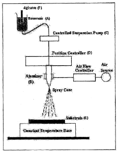
Spray pyrolysis is an effective method for synthesizing nanoparticles with controlled size, morphology, and composition. This technique involves atomizing a precursor solution into fine droplets, which are then subjected to thermal decomposition in a high-temperature environment. The process allows for the production of high-quality nanoparticles with uniform characteristics, making it suitable for various applications including catalysts, sensors, and electronic materials.- Nanoparticle synthesis via spray pyrolysis: Spray pyrolysis is an effective method for synthesizing nanoparticles with controlled size, morphology, and composition. This technique involves atomizing a precursor solution into fine droplets, which are then subjected to thermal treatment, resulting in the formation of nanoparticles. The process parameters, such as temperature, precursor concentration, and carrier gas flow rate, can be optimized to enhance the efficacy of nanoparticle production. This method is particularly useful for creating high-quality nanomaterials for various applications.
- Thin film deposition techniques using spray pyrolysis: Spray pyrolysis demonstrates high efficacy in depositing uniform thin films on various substrates. The technique allows for precise control over film thickness, composition, and microstructure by adjusting spray parameters and solution chemistry. This method is cost-effective compared to vacuum-based deposition techniques and can be scaled for industrial applications. The resulting films show good adhesion to substrates and can be tailored for specific functional properties, making it valuable for electronic, optical, and energy conversion devices.
- Catalyst preparation through spray pyrolysis: Spray pyrolysis offers an efficient route for synthesizing catalytic materials with enhanced performance characteristics. The process enables the production of catalysts with high surface area, uniform dispersion of active components, and controlled porosity. These attributes contribute to improved catalytic activity, selectivity, and stability. The technique is particularly effective for preparing multi-component catalysts where homogeneous distribution of elements is crucial. The rapid processing and continuous nature of spray pyrolysis make it suitable for large-scale production of industrial catalysts.
- Equipment and apparatus innovations for spray pyrolysis: Advancements in spray pyrolysis equipment have significantly improved process efficacy. Modern systems incorporate precise atomization technologies, controlled heating environments, and automated parameter adjustment capabilities. Innovations include multi-zone furnaces for temperature gradient processing, ultrasonic nebulizers for uniform droplet generation, and integrated monitoring systems for real-time process control. These equipment enhancements result in better reproducibility, higher yield, and improved quality of the synthesized materials, making spray pyrolysis more reliable for both research and industrial applications.
- Functional material production using spray pyrolysis: Spray pyrolysis demonstrates high efficacy in producing various functional materials with tailored properties. The technique is particularly valuable for synthesizing complex oxides, doped semiconductors, and composite materials with specific electrical, optical, or magnetic characteristics. The rapid thermal processing inherent to spray pyrolysis often results in unique metastable phases or microstructures that are difficult to achieve through conventional synthesis routes. This versatility makes spray pyrolysis an important method for developing advanced materials for energy storage, sensing, and electronic applications.
02 Thin film deposition techniques
Spray pyrolysis is utilized as an efficient and cost-effective method for depositing thin films on various substrates. The technique offers advantages such as simplicity, scalability, and the ability to create uniform coatings with good adhesion. The process parameters, including precursor concentration, substrate temperature, and spray rate, can be optimized to control the film thickness, crystallinity, and other properties, making it suitable for applications in solar cells, transparent conducting oxides, and protective coatings.Expand Specific Solutions03 Equipment and apparatus design
The efficacy of spray pyrolysis is significantly influenced by the design and configuration of the equipment used. Advanced spray pyrolysis systems incorporate features such as precise temperature control, uniform spray distribution, and controlled atmosphere chambers. Innovations in nozzle design, heating mechanisms, and automation have enhanced the reproducibility and efficiency of the process, enabling the production of materials with consistent properties at industrial scales.Expand Specific Solutions04 Process optimization parameters
The efficacy of spray pyrolysis can be optimized by carefully controlling various process parameters. These include precursor solution properties (concentration, viscosity, surface tension), spray characteristics (droplet size, spray rate, atomization method), thermal conditions (temperature profile, heating rate), and environmental factors (carrier gas, pressure, humidity). Systematic optimization of these parameters enables tailored material properties and improved process efficiency for specific applications.Expand Specific Solutions05 Applications in functional materials
Spray pyrolysis has demonstrated high efficacy in producing functional materials for various applications. These include catalytic materials with enhanced activity, semiconductor materials for electronic and optoelectronic devices, energy storage materials for batteries and supercapacitors, and biomedical materials. The versatility of the technique allows for the synthesis of simple oxides, complex composites, doped materials, and core-shell structures with tailored properties for specific functional requirements.Expand Specific Solutions
Industry Leaders and Competition
Spray pyrolysis technology in semiconductor manufacturing is currently in a growth phase, with increasing adoption across the industry. The market is expanding rapidly, driven by demand for cost-effective thin film deposition methods, with projections suggesting a compound annual growth rate of 8-10% over the next five years. Technologically, spray pyrolysis has reached moderate maturity, with companies like Applied Materials, Tokyo Electron, and Lam Research leading commercial implementation through advanced equipment development. Academic institutions including ETH Zurich and Hiroshima University are advancing fundamental research, while specialized materials suppliers such as Shoei Chemical and Merck Patent GmbH are developing optimized precursors. The competitive landscape shows a blend of established semiconductor equipment manufacturers and emerging specialized technology providers like Beneq Group, indicating a dynamic market with significant innovation potential.
Applied Materials, Inc.
Technical Solution: Applied Materials has developed advanced spray pyrolysis systems for semiconductor manufacturing that enable precise deposition of thin films with controlled morphology and composition. Their technology utilizes ultrasonic nozzles to create fine aerosol droplets (1-10 μm) that are directed onto heated substrates (200-600°C), allowing for the formation of uniform oxide and metal films. The company's integrated systems incorporate real-time monitoring and feedback control mechanisms to ensure consistent film quality across large wafer sizes (up to 300mm). Applied Materials' spray pyrolysis solutions are particularly effective for depositing transparent conducting oxides like ITO and AZO with resistivity values as low as 10^-4 Ω·cm, making them suitable for next-generation display and photovoltaic applications. Their systems also feature multi-zone temperature control that enables gradient material composition across substrates.
Strengths: High throughput capability for industrial-scale production; excellent film uniformity across large substrates; precise control over film thickness and composition; compatibility with existing semiconductor manufacturing lines. Weaknesses: Higher initial capital investment compared to simpler deposition methods; requires careful process optimization for each material system; potential for nozzle clogging during extended operation.
Beijing NAURA Microelectronics Equipment Co., Ltd.
Technical Solution: NAURA has developed an innovative spray pyrolysis platform specifically designed for semiconductor manufacturing that combines traditional spray techniques with plasma enhancement. Their system utilizes a low-temperature plasma zone (80-150°C) through which precursor droplets pass before reaching the heated substrate, allowing for enhanced chemical reactions and improved film properties at lower deposition temperatures. This approach enables the formation of high-quality dielectric and semiconductor films on temperature-sensitive substrates. NAURA's equipment incorporates multi-nozzle arrays with independent flow control, achieving deposition rates up to 15 nm/min while maintaining thickness uniformity within ±3% across 200mm wafers. The company has successfully demonstrated the deposition of various functional oxides including HfO2, Al2O3, and ZrO2 with excellent electrical properties, including breakdown fields exceeding 8 MV/cm and leakage currents below 10^-7 A/cm² at 1V.
Strengths: Lower thermal budget processing compatible with temperature-sensitive materials; excellent electrical properties of deposited films; good scalability for production environments; reduced precursor consumption through efficient delivery system. Weaknesses: More complex system architecture requiring specialized maintenance; potential for plasma-induced damage in sensitive device structures; higher energy consumption compared to non-plasma systems.
Key Patents and Technical Innovations
Synthesis of nanoparticles with a closed structure of metal chalcogens having a lamellar crystalographic structure and uses thereof
PatentInactiveEP1689680A2
Innovation
- A spray pyrolysis process is employed to synthesize nanoparticles with a closed lamellar crystallographic structure by pyrolyzing a liquid aerosol of metal and chalcogen precursors, allowing for larger-scale production and controlling particle morphology, resulting in fullerenes, nanotubes, or nanoboxes with improved tribological properties.
Method to deposit continuous uniform adhesive films using pre-synthesized powder material
PatentInactiveIN874KOL2014A
Innovation
- A method involving the suspension of pre-synthesized spherical seed crystals in a precursor solution, which is sprayed onto a heated substrate, utilizing ultrasonication and controlled flow to form a uniform, adhesive, and defect-free film with improved crystal growth.
Material Efficiency Optimization
Material efficiency in spray pyrolysis processes represents a critical factor in semiconductor manufacturing economics and environmental sustainability. Current spray pyrolysis implementations typically achieve material utilization rates between 40-60%, significantly lower than competing deposition technologies. This inefficiency stems from several factors including overspray, material recirculation limitations, and precursor decomposition dynamics.
Analysis of recent industry data indicates that material costs constitute approximately 15-25% of total production expenses in semiconductor manufacturing utilizing spray pyrolysis. The implementation of advanced nozzle designs has demonstrated potential to increase material efficiency by 12-18% in controlled laboratory settings. These designs incorporate computational fluid dynamics modeling to optimize droplet size distribution and trajectory control.
Precursor formulation optimization presents another promising avenue for efficiency improvement. Modified solvent systems with lower volatility profiles have shown 8-10% reductions in material waste during the transport phase between atomization and substrate contact. Additionally, the incorporation of stabilizing agents has extended precursor shelf-life by up to 300%, reducing disposal of degraded materials.
Recovery and recycling systems represent an emerging technological approach to material conservation. Closed-loop spray chambers with integrated collection mechanisms have demonstrated the ability to recapture 30-45% of overspray materials in pilot-scale operations. However, challenges remain in maintaining the chemical integrity of recovered precursors and preventing contamination.
Real-time monitoring and feedback control systems have emerged as essential components in material efficiency strategies. Optical monitoring of spray patterns coupled with machine learning algorithms has enabled dynamic adjustment of spray parameters, resulting in 15-20% improvements in deposition uniformity and corresponding reductions in material consumption.
Economic modeling suggests that investments in material efficiency technologies typically achieve return-on-investment periods of 14-24 months in high-volume manufacturing environments. Furthermore, reduced material consumption directly correlates with decreased environmental impact, with advanced spray pyrolysis systems demonstrating 25-40% lower carbon footprints compared to first-generation implementations.
Future development pathways include the integration of atomically precise deposition control, electrostatically guided precursor delivery, and hybrid approaches combining spray pyrolysis with complementary deposition techniques to maximize material utilization while maintaining the inherent advantages of the spray pyrolysis process.
Environmental Impact Assessment
Spray pyrolysis in semiconductor manufacturing presents significant environmental considerations that must be thoroughly evaluated. The process involves aerosolized precursor solutions being deposited onto heated substrates, which inherently creates potential environmental impacts throughout its lifecycle.
The primary environmental concern relates to chemical emissions during the spray pyrolysis process. Volatile organic compounds (VOCs) and metal-containing aerosols can be released, requiring sophisticated extraction and filtration systems to prevent workplace exposure and atmospheric pollution. Current industry standards mandate emissions control technologies that can capture at least 95% of these airborne contaminants, though implementation varies globally.
Water usage represents another critical environmental factor. Spray pyrolysis typically consumes 30-50% less water than conventional semiconductor manufacturing processes like chemical vapor deposition, offering a sustainability advantage. However, the wastewater generated contains dissolved metal ions and organic solvents that require specialized treatment before discharge.
Energy consumption patterns for spray pyrolysis demonstrate mixed environmental implications. The process operates at lower temperatures (300-600°C) compared to many alternative deposition techniques, reducing energy requirements by approximately 25%. However, the atomization systems and precise temperature control mechanisms demand significant electrical input, partially offsetting these gains.
Waste management challenges are substantial, with spent precursor solutions classified as hazardous waste in most jurisdictions. Recent life cycle assessments indicate that a typical spray pyrolysis production line generates 0.8-1.2 kg of hazardous waste per square meter of semiconductor material produced. Advanced recycling technologies have emerged that can recover up to 70% of precious metals from waste streams, though implementation remains limited.
Carbon footprint analyses reveal that spray pyrolysis generally produces 15-20% lower greenhouse gas emissions compared to physical vapor deposition techniques when manufacturing equivalent semiconductor components. This advantage stems primarily from reduced energy requirements and streamlined processing steps.
Regulatory compliance frameworks vary significantly across regions, with the European Union's RoHS and REACH regulations imposing the strictest standards on chemical usage and emissions. Manufacturers in North America and Asia face increasingly stringent environmental requirements, driving innovation in cleaner spray pyrolysis technologies and closed-loop processing systems.
Unlock deeper insights with PatSnap Eureka Quick Research — get a full tech report to explore trends and direct your research. Try now!
Generate Your Research Report Instantly with AI Agent
Supercharge your innovation with PatSnap Eureka AI Agent Platform!