

GaN HEMT Role In High-Performance Computing Infrastructure
SEP 8, 20259 MIN READ
Generate Your Research Report Instantly with AI Agent
PatSnap Eureka helps you evaluate technical feasibility & market potential.
GaN HEMT Evolution and Computing Performance Goals
Gallium Nitride High Electron Mobility Transistors (GaN HEMTs) have undergone remarkable evolution since their inception in the early 1990s. Initially developed for military and aerospace applications due to their superior performance in high-power, high-frequency operations, GaN HEMTs have progressively transitioned into commercial applications. The technology has evolved from basic laboratory demonstrations to sophisticated commercial products, with significant improvements in power density, efficiency, and reliability over the past three decades.
The evolution trajectory of GaN HEMTs has been characterized by continuous advancements in epitaxial growth techniques, device architecture optimization, and thermal management solutions. Early GaN HEMTs suffered from current collapse and reliability issues, which have been systematically addressed through innovations such as field plates, passivation techniques, and advanced substrate technologies. The transition from silicon carbide to silicon substrates has been particularly significant in reducing manufacturing costs while maintaining performance advantages.
In the context of high-performance computing (HPC) infrastructure, GaN HEMTs are increasingly recognized as critical components for next-generation power delivery systems. As computing workloads become more intensive and data centers expand, traditional silicon-based power solutions are approaching their theoretical limits in terms of efficiency and power density. GaN technology offers a compelling alternative with switching frequencies exceeding 1 MHz and efficiencies above 98% in power conversion applications.
The performance goals for GaN HEMTs in HPC applications are multifaceted. Primary objectives include achieving power densities exceeding 10 kW/cm³ in server power supplies, reducing conversion losses by more than 50% compared to silicon alternatives, and enabling operation at junction temperatures above 200°C with minimal performance degradation. Additionally, there is a strong focus on improving reliability metrics to achieve mean time between failures (MTBF) exceeding 10 million hours, which is essential for mission-critical computing infrastructure.
Looking forward, the technology roadmap for GaN HEMTs in HPC applications emphasizes vertical device architectures to further increase breakdown voltage and current handling capabilities. Integration with advanced packaging technologies, including embedded cooling solutions and 3D integration with silicon logic, represents another frontier. The ultimate goal is to enable a paradigm shift in power delivery architectures for computing systems, moving from centralized to distributed topologies that can significantly improve overall system efficiency and performance.
The convergence of GaN HEMT technology with artificial intelligence accelerators and quantum computing systems presents particularly promising opportunities. These emerging computing paradigms demand unprecedented power delivery performance, where GaN's superior switching characteristics and thermal properties could prove transformative in overcoming current limitations in computational density and energy efficiency.
Market Demand for GaN-Based HPC Solutions
The global High-Performance Computing (HPC) market is experiencing unprecedented growth, driven by increasing demands for computational power across various sectors. This growth trajectory has created a significant market opportunity for Gallium Nitride (GaN) High Electron Mobility Transistor (HEMT) technology. Current market analyses indicate that the HPC infrastructure market is expected to reach $44 billion by 2025, with power management solutions representing approximately 15% of this value.
The demand for GaN-based HPC solutions stems primarily from four key market segments. First, data centers are facing critical challenges in power efficiency as they scale to meet cloud computing demands. These facilities currently consume about 1-2% of global electricity, with cooling systems accounting for up to 40% of their energy usage. GaN HEMT technology offers potential energy savings of 30-40% compared to silicon-based solutions, representing a compelling value proposition for data center operators seeking to reduce operational costs.
Second, the supercomputing sector requires increasingly efficient power delivery systems to support exascale computing capabilities. Current supercomputers consume megawatts of power, with significant performance limitations due to thermal constraints. Market research indicates that institutions are willing to invest substantially in technologies that can deliver higher computational density per watt, creating a premium market segment for GaN solutions.
Third, the artificial intelligence and machine learning sector has emerged as a major driver for advanced computing infrastructure. The training of large AI models requires massive computational resources, with energy consumption becoming a limiting factor. Industry reports suggest that companies are allocating increasing portions of their R&D budgets to more efficient computing architectures, with power management being a critical consideration.
Fourth, edge computing applications represent a rapidly growing market segment where power efficiency is paramount. With the proliferation of IoT devices and the need for distributed computing resources, compact and efficient power solutions are essential. GaN HEMT technology's ability to operate at higher frequencies while maintaining efficiency makes it particularly suitable for these applications.
Market surveys indicate that end-users are increasingly prioritizing Total Cost of Ownership (TCO) over initial capital expenditure, creating favorable conditions for GaN technology adoption despite higher upfront costs. Additionally, regulatory pressures and corporate sustainability initiatives are driving demand for more energy-efficient computing solutions, with several major technology companies committing to carbon-neutral operations within the next decade.
GaN HEMT Technology Status and Challenges
Gallium Nitride High Electron Mobility Transistors (GaN HEMTs) have emerged as a revolutionary technology in power electronics, with significant implications for high-performance computing infrastructure. Currently, GaN HEMT technology has reached commercial maturity in RF applications but is still evolving rapidly for power switching applications in computing environments. The wide bandgap properties of GaN (3.4 eV compared to silicon's 1.1 eV) enable higher breakdown voltages, faster switching speeds, and superior thermal conductivity, making it particularly suitable for next-generation data centers and computing facilities.
Globally, GaN HEMT development shows distinct regional characteristics. The United States leads in fundamental research and military applications, with institutions like MIT, Stanford, and companies such as Wolfspeed and Qorvo driving innovation. Europe focuses on automotive and industrial applications through companies like Infineon and STMicroelectronics. Meanwhile, Asia, particularly Japan (Panasonic, Toshiba) and China (SANAN, HiWafer), is rapidly expanding manufacturing capacity and developing specialized applications for computing infrastructure.
Despite significant progress, GaN HEMT technology faces several critical challenges that limit its widespread adoption in high-performance computing. The most pressing technical obstacle remains the "current collapse" phenomenon—a temporary reduction in drain current after high-voltage operation that affects reliability in computing applications. Additionally, dynamic ON-resistance degradation continues to impact efficiency in high-switching-frequency scenarios typical in modern data centers.
Manufacturing scalability presents another significant hurdle. The production of high-quality GaN epitaxial layers on large-diameter substrates remains difficult, with defect densities still higher than ideal for computing-grade reliability. The industry continues to struggle with cost-effective solutions for 8-inch and larger wafer production, which is essential for competitive pricing against silicon alternatives.
Thermal management represents a persistent challenge, particularly in densely packed computing environments. While GaN inherently offers better thermal properties than silicon, the extreme power densities in modern computing applications require innovative packaging and cooling solutions that are still under development. Current thermal interface materials and heat dissipation techniques are inadequate for maximizing GaN HEMT potential in high-performance computing infrastructure.
Standardization and reliability qualification frameworks specific to GaN in computing applications remain underdeveloped. Unlike silicon technologies with decades of established reliability protocols, GaN HEMT qualification for computing infrastructure lacks industry-wide consensus, creating barriers to adoption by conservative data center operators and computing hardware manufacturers.
Integration challenges with existing silicon-based computing architectures represent another significant obstacle. The different driving requirements, voltage levels, and control mechanisms of GaN HEMTs require substantial modifications to conventional computing power delivery architectures, necessitating new design approaches and potentially hybrid solutions during the transition period.
Current GaN HEMT Implementation in Data Centers
01 GaN HEMT device structure and fabrication
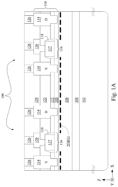
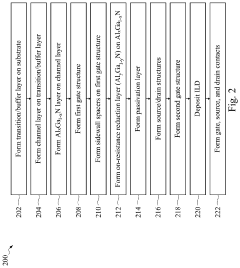
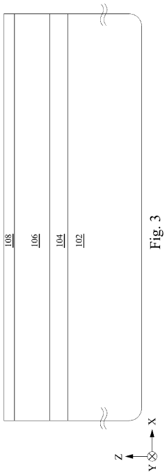
GaN HEMT devices are fabricated with specific structural elements to optimize performance. These include the arrangement of layers such as the buffer layer, channel layer, barrier layer, and gate structure. Advanced fabrication techniques focus on reducing defects, improving crystal quality, and enhancing carrier mobility in the two-dimensional electron gas (2DEG) channel. Various substrate materials and epitaxial growth methods are employed to achieve high-quality GaN-based transistor structures.- GaN HEMT device structure and fabrication: Gallium Nitride High Electron Mobility Transistors (GaN HEMTs) have specific structural designs that enhance their performance. These devices typically include multiple layers such as buffer layers, channel layers, barrier layers, and specialized gate structures. The fabrication process involves techniques like epitaxial growth, etching, and metallization to create these high-performance semiconductor devices. Various structural innovations help to improve electron mobility and reduce parasitic effects.
- Power management and efficiency improvements: GaN HEMTs offer significant advantages in power management applications due to their high breakdown voltage, low on-resistance, and fast switching capabilities. Innovations in this area focus on reducing power losses, improving thermal management, and enhancing overall efficiency. These improvements enable GaN HEMTs to operate at higher frequencies and power densities compared to traditional silicon-based devices, making them ideal for power conversion applications.
- RF and microwave applications: GaN HEMTs excel in radio frequency (RF) and microwave applications due to their high electron mobility and power density. Innovations in this category focus on improving linearity, gain, and noise characteristics for applications in telecommunications, radar systems, and satellite communications. Specialized designs optimize the devices for different frequency bands and power requirements, enabling higher data rates and longer range in wireless systems.
- Reliability and performance enhancement techniques: Improving the reliability and long-term performance of GaN HEMTs is critical for their commercial adoption. This includes addressing issues such as current collapse, gate leakage, and thermal degradation. Various passivation techniques, surface treatments, and field plate designs are employed to enhance device stability under high-voltage and high-temperature conditions. These enhancements extend device lifetime and maintain consistent performance under stress conditions.
- Integration and packaging solutions: Effective integration of GaN HEMTs into practical systems requires specialized packaging and integration techniques. This includes addressing thermal management challenges, electromagnetic interference, and parasitic effects. Advanced packaging solutions enable higher power density while maintaining reliability. Integration with control circuitry and other components allows for compact, high-performance modules suitable for various applications including power supplies, motor drives, and RF amplifiers.
02 Power electronics applications of GaN HEMTs
GaN HEMTs are increasingly utilized in power electronics due to their high breakdown voltage, low on-resistance, and fast switching capabilities. These devices enable more efficient power conversion systems for applications including power supplies, motor drives, and renewable energy systems. The wide bandgap properties of GaN allow for operation at higher voltages, temperatures, and frequencies compared to silicon-based devices, resulting in smaller, more efficient power electronic systems.Expand Specific Solutions03 RF and microwave applications of GaN HEMTs
GaN HEMTs excel in radio frequency (RF) and microwave applications due to their high electron mobility, high power density, and excellent frequency response. These transistors are used in wireless communication systems, radar systems, and satellite communications. The ability to operate at high frequencies while handling significant power levels makes them ideal for RF power amplifiers in base stations, defense systems, and other high-frequency applications requiring robust performance.Expand Specific Solutions04 Reliability and thermal management of GaN HEMTs
Ensuring reliability and effective thermal management are critical challenges in GaN HEMT technology. Various approaches address issues such as current collapse, gate leakage, and thermal degradation. Advanced packaging techniques, heat spreading materials, and optimized device layouts help manage the high power densities generated during operation. Passivation layers and field plates are employed to mitigate electric field concentrations and improve long-term stability under high-voltage and high-temperature conditions.Expand Specific Solutions05 Novel materials and structures for enhanced GaN HEMT performance
Research focuses on incorporating novel materials and structural innovations to enhance GaN HEMT performance. This includes the development of advanced barrier layers, novel gate architectures, and integration of complementary materials. Techniques such as polarization engineering, heterojunction optimization, and surface treatment methods are employed to improve electron mobility, reduce parasitic effects, and enhance overall device efficiency. These innovations aim to push the boundaries of what is possible with GaN HEMT technology.Expand Specific Solutions
Key Industry Players in GaN HEMT Manufacturing
The GaN HEMT market in high-performance computing infrastructure is in a growth phase, with increasing adoption driven by superior power efficiency and thermal performance compared to silicon-based technologies. The market is expanding rapidly as data centers seek energy-efficient solutions, with projections indicating significant growth over the next five years. Leading semiconductor manufacturers like Texas Instruments, QUALCOMM, and Fujitsu are advancing GaN HEMT technology, while research institutions such as Xidian University and The Hong Kong University of Science & Technology contribute to innovation. Companies including Huawei, GlobalFoundries, and United Microelectronics are developing commercial applications, with varying degrees of technological maturity across power management, RF applications, and high-frequency computing domains.
Texas Instruments Incorporated
Technical Solution: Texas Instruments has developed comprehensive GaN HEMT solutions specifically targeting high-performance computing power infrastructure. Their approach centers on highly integrated GaN power stages that combine drivers, protection circuitry, and GaN HEMTs in single packages optimized for server and data center applications. TI's implementation features their proprietary GaN process technology that enables operation at 600-650V with enhanced reliability through specialized passivation techniques and optimized field plates. Their GaN solutions achieve switching frequencies of 1-2MHz while maintaining efficiency above 98% across wide load ranges, critical for the variable workloads in computing environments. TI has also pioneered advanced packaging techniques for GaN devices that minimize parasitic inductances, enabling faster switching transitions with reduced ringing and EMI. Their GaN controllers incorporate specialized algorithms that dynamically adjust switching parameters based on load conditions, maximizing efficiency while ensuring reliability. TI's solutions have demonstrated power density improvements of 3-4x compared to silicon-based alternatives in server power supplies.
Strengths: TI's vertical integration from semiconductor fabrication through system design enables highly optimized GaN solutions. Their extensive power management expertise allows for sophisticated control algorithms specifically tailored to GaN characteristics. Weaknesses: Their GaN technology currently focuses primarily on power conversion rather than RF applications, potentially limiting applications in certain computing communication infrastructure.
QUALCOMM, Inc.
Technical Solution: Qualcomm has pioneered the integration of GaN HEMT technology in their high-performance computing solutions, focusing particularly on edge computing applications where power efficiency is critical. Their approach leverages GaN HEMT's superior switching characteristics to develop more efficient power delivery networks for their Snapdragon platforms used in AI acceleration and edge computing. Qualcomm's implementation features specialized circuit designs that capitalize on GaN's higher breakdown voltage and lower on-resistance, enabling more compact and efficient power solutions. Their GaN HEMT-based power systems operate at switching frequencies of 3-5MHz, significantly higher than silicon alternatives, allowing for smaller inductors and capacitors. This has enabled Qualcomm to achieve power densities exceeding 1000W/in³ in their latest computing modules. The company has also developed advanced thermal management techniques specifically for GaN devices, including dynamic thermal regulation algorithms that optimize performance under varying computational loads.
Strengths: Qualcomm's expertise in mobile and edge computing positions them uniquely to leverage GaN HEMT benefits in distributed computing architectures. Their system-level integration approach maximizes GaN's advantages across the entire computing platform. Weaknesses: Their focus remains primarily on edge computing rather than large-scale data center infrastructure, potentially limiting impact in centralized HPC environments.
Critical Patents and Breakthroughs in GaN HEMT Design
Gallium nitride high electron mobility transistor having high breakdown voltage and formation method therefor
PatentInactiveEP3591708A1
Innovation
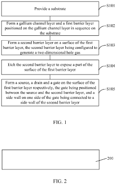
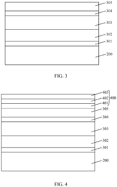
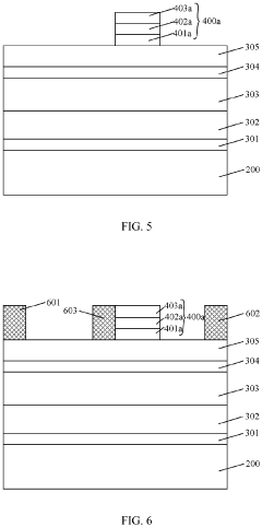
- A gallium nitride high electron mobility transistor with a second barrier layer configured to generate two-dimensional hole gas, positioned between the gate and drain, smoothes electric field distribution and improves breakdown voltage, comprising a substrate, gallium nitride channel layer, first and second barrier layers, and source and drain structures.
Gallium nitride high electron mobility transistor
PatentPendingUS20230395694A1
Innovation
- The solution involves forming a second AlGaN layer with a different composition over the AlGaN-GaN heterojunction, using sidewall spacers and selective epitaxy to decouple on-resistance from the threshold voltage, achieved by increasing the aluminum concentration in the AlGaN layer and adjusting its thickness, thereby enhancing spontaneous and piezoelectric polarization effects.
Thermal Management Solutions for GaN HEMT in HPC
Thermal management represents a critical challenge in the integration of GaN HEMT technology into high-performance computing (HPC) infrastructure. As power densities continue to increase in modern HPC systems, effective heat dissipation becomes paramount for maintaining device reliability and performance. GaN HEMTs, despite their superior electrical properties, generate significant heat during operation, with power densities exceeding 5 W/mm², approximately five times higher than traditional silicon-based devices.
Current thermal management solutions for GaN HEMTs in HPC environments employ multi-faceted approaches. Advanced packaging techniques utilizing diamond-based substrates have demonstrated thermal conductivity values up to 2000 W/mK, significantly outperforming traditional silicon carbide substrates (370 W/mK). These materials facilitate more efficient heat transfer from the active device region to heat sinks and cooling systems.
Microfluidic cooling channels integrated directly into GaN HEMT packages represent another innovative solution. These channels allow coolant to flow in close proximity to heat-generating regions, achieving thermal resistances below 0.1°C·cm²/W. Implementation of two-phase cooling systems utilizing refrigerants like R-1234ze provides enhanced cooling capacity through latent heat absorption during phase change, enabling heat flux handling capabilities exceeding 500 W/cm².
Computational fluid dynamics (CFD) modeling has become essential for optimizing thermal management designs. Advanced simulation tools now incorporate multi-physics capabilities that simultaneously model electrical, thermal, and mechanical behaviors of GaN devices in HPC environments, enabling more precise thermal solution development tailored to specific operational conditions.
Novel thermal interface materials (TIMs) with graphene and carbon nanotube composites have emerged as promising solutions, offering thermal conductivities up to 25 W/mK while maintaining the mechanical compliance necessary for reliable thermal contacts. These materials significantly reduce thermal boundary resistance at critical interfaces within the thermal stack.
System-level approaches include dynamic thermal management through intelligent power distribution algorithms that monitor temperature across HPC clusters and redistribute computational loads to prevent hotspots. Combined with advanced liquid cooling infrastructure utilizing dielectric fluids, these systems can maintain junction temperatures below 85°C even under peak computational loads.
Recent developments in additive manufacturing have enabled the creation of optimized heat sink geometries with complex internal structures that maximize surface area while minimizing fluid flow resistance, resulting in cooling efficiency improvements of 30-40% compared to conventional designs.
Energy Efficiency Impact and Carbon Footprint Reduction
The integration of Gallium Nitride High Electron Mobility Transistors (GaN HEMTs) into high-performance computing (HPC) infrastructure represents a significant advancement in addressing energy efficiency challenges. GaN HEMTs offer superior power conversion efficiency compared to traditional silicon-based technologies, with demonstrated improvements of 30-40% in power supply units and voltage regulators critical to data center operations.
This enhanced efficiency directly translates to reduced energy consumption across computing facilities. For a typical hyperscale data center consuming 100MW of power, GaN HEMT implementation in power delivery systems can potentially reduce energy usage by 10-15MW, resulting in substantial operational cost savings and decreased strain on electrical grids. The cascading effect of this efficiency extends beyond direct power consumption to cooling requirements, which typically account for 40% of data center energy usage.
The carbon footprint implications are equally significant. Based on current global average carbon intensity of electricity generation (approximately 475g CO2/kWh), GaN HEMT adoption across major cloud computing providers could reduce carbon emissions by millions of metric tons annually. Microsoft's recent pilot implementations have demonstrated a potential 17% reduction in server farm carbon footprint through GaN-based power solutions.
From a lifecycle perspective, GaN HEMTs contribute to sustainability through their smaller form factor and reduced material requirements. The higher power density allows for more compact designs, decreasing the embodied carbon associated with manufacturing and transportation. Additionally, the superior thermal performance reduces cooling infrastructure needs, further diminishing the environmental impact of HPC facilities.
Economic analyses indicate that despite higher initial component costs, GaN HEMT implementation achieves positive return on investment within 18-24 months through energy savings alone. This favorable economics accelerates adoption across the computing industry, amplifying the aggregate environmental benefits. Several major cloud service providers have already committed to GaN-based power systems as part of their carbon neutrality roadmaps.
The regulatory landscape increasingly favors such efficiency improvements, with initiatives like the EU's Energy Efficiency Directive and the US Department of Energy's data center efficiency standards creating additional incentives for GaN HEMT adoption. These policy frameworks, combined with corporate sustainability commitments, are accelerating the transition toward more energy-efficient computing infrastructure powered by wide-bandgap semiconductor technologies like GaN.
Unlock deeper insights with PatSnap Eureka Quick Research — get a full tech report to explore trends and direct your research. Try now!
Generate Your Research Report Instantly with AI Agent
Supercharge your innovation with PatSnap Eureka AI Agent Platform!