

GaN HEMT Testing Techniques For High-Power Applications
SEP 8, 20259 MIN READ
Generate Your Research Report Instantly with AI Agent
PatSnap Eureka helps you evaluate technical feasibility & market potential.
GaN HEMT Evolution and Testing Objectives
Gallium Nitride High Electron Mobility Transistors (GaN HEMTs) have emerged as revolutionary semiconductor devices for high-power applications, evolving significantly since their inception in the early 1990s. The evolution of GaN HEMT technology has been driven by the inherent material advantages of GaN, including wide bandgap (3.4 eV), high breakdown field strength (3.3 MV/cm), and superior electron mobility. These properties enable GaN HEMTs to operate at higher voltages, frequencies, and temperatures compared to silicon-based devices, making them ideal candidates for power electronics, RF amplifiers, and radar systems.
The developmental trajectory of GaN HEMTs has progressed through several critical phases. Initially, research focused on fundamental material growth techniques and basic device structures. This was followed by advancements in epitaxial layer optimization and device architecture refinements to address challenges such as current collapse and dynamic on-resistance. Recent years have witnessed significant improvements in reliability engineering and thermal management solutions, enabling GaN HEMTs to meet the stringent requirements of high-power applications.
As GaN HEMT technology matures and finds increasing adoption in commercial and military applications, the need for comprehensive and standardized testing methodologies has become paramount. Current testing objectives primarily focus on characterizing device performance under extreme operating conditions, including high voltage stress, high current density, and elevated temperatures. These tests aim to evaluate critical parameters such as breakdown voltage, on-resistance, transconductance, and thermal resistance.
Another crucial testing objective involves reliability assessment, particularly accelerated life testing to predict long-term device behavior. This includes tests for time-dependent dielectric breakdown (TDDB), hot electron effects, and electromigration. For high-power applications specifically, testing must address unique challenges such as current collapse phenomena, trapping effects, and thermal management under pulsed operation conditions.
The industry trend is moving toward developing standardized testing protocols that can accurately predict device performance in real-world applications. This includes dynamic characterization techniques that can capture transient effects during switching events, which are particularly relevant for power conversion applications. Additionally, there is growing emphasis on developing non-destructive testing methods that can identify potential failure mechanisms before catastrophic device failure occurs.
Looking forward, testing objectives are expanding to include evaluation of GaN HEMTs in system-level contexts, assessing their interaction with gate drivers, protection circuits, and passive components. The ultimate goal is to establish comprehensive testing frameworks that can accelerate the qualification process for GaN HEMT devices in high-reliability applications such as automotive, aerospace, and industrial power systems, where failure is not an option and performance must be guaranteed across extreme operating conditions.
Market Demand for High-Power GaN HEMT Solutions
The global market for high-power GaN HEMT solutions has witnessed substantial growth in recent years, driven primarily by increasing demands in telecommunications, defense, aerospace, and industrial applications. The transition from silicon-based power devices to GaN technology is accelerating due to GaN's superior properties, including higher breakdown voltage, faster switching speeds, and better thermal conductivity.
In the telecommunications sector, the rollout of 5G infrastructure has created significant demand for high-power GaN HEMT solutions. Base stations require power amplifiers capable of handling higher frequencies and power levels while maintaining efficiency. Market research indicates that the 5G infrastructure market is expected to grow at a compound annual growth rate of over 40% through 2025, directly driving demand for GaN HEMT devices.
Defense and aerospace applications represent another substantial market segment. Radar systems, electronic warfare equipment, and satellite communications all benefit from GaN HEMT technology's high-power density and reliability in harsh environments. The defense electronics market specifically related to GaN technology has been growing steadily, with military organizations worldwide investing in next-generation communication and radar systems.
The automotive industry is emerging as a promising market for GaN HEMT solutions, particularly with the rapid development of electric vehicles (EVs). Power conversion systems in EVs require efficient, compact, and reliable components—characteristics inherent to GaN technology. As EV production continues to scale globally, the demand for advanced power electronics is projected to increase substantially.
Industrial applications, including power supplies, motor drives, and renewable energy systems, are also driving market growth. The push for greater energy efficiency and power density in industrial equipment has positioned GaN HEMTs as ideal replacements for traditional silicon-based solutions. The industrial power electronics segment utilizing GaN technology has been growing at approximately 25% annually.
Testing techniques for high-power GaN HEMTs have become increasingly critical as applications demand higher reliability and performance. Market analysis shows that companies are willing to invest significantly in advanced testing equipment and methodologies to ensure device quality and longevity. The test and measurement equipment market specifically for wide-bandgap semiconductors has been expanding rapidly to meet these needs.
Regional analysis indicates that North America and Asia-Pacific currently lead in GaN HEMT adoption, with Europe showing accelerated growth. China's strategic focus on semiconductor independence has resulted in substantial investments in GaN technology development and testing capabilities, creating a dynamic market landscape with both established players and emerging competitors.
Current Testing Challenges for GaN HEMTs
Testing Gallium Nitride High Electron Mobility Transistors (GaN HEMTs) for high-power applications presents several significant challenges that impede comprehensive performance evaluation and reliability assessment. The wide bandgap semiconductor properties that make GaN HEMTs attractive for high-power applications simultaneously create unique testing difficulties not encountered with traditional silicon-based devices.
One primary challenge is thermal management during testing. GaN HEMTs operate at significantly higher power densities and temperatures than silicon devices, often exceeding 250°C at the junction. This extreme thermal environment complicates accurate measurement as conventional test equipment and methodologies may not be designed to handle such conditions. The thermal resistance characterization becomes particularly problematic as heat dissipation pathways in GaN devices differ substantially from silicon counterparts.
Dynamic performance testing presents another major hurdle. GaN HEMTs exhibit extremely fast switching speeds with slew rates exceeding 100V/ns, which conventional test equipment struggles to capture accurately. The parasitic inductances in test fixtures can significantly distort measurement results, leading to incorrect characterization of switching losses and transient behaviors that are critical for high-power applications.
Current collapse and dispersion effects represent particularly challenging phenomena to quantify during testing. These effects, where device performance degrades under high-voltage switching conditions, are highly dependent on operating history and environmental factors. Standard DC characterization fails to capture these dynamic effects, necessitating specialized pulsed I-V measurements that many test systems are not equipped to perform with sufficient accuracy.
Reliability testing faces substantial obstacles due to the novel failure mechanisms in GaN technology. Traditional silicon-based accelerated life testing protocols may not accurately predict GaN HEMT reliability. The industry lacks standardized testing methodologies specifically developed for GaN technology, creating inconsistencies in reliability data across different manufacturers and research institutions.
High-voltage isolation during testing constitutes another significant challenge. With breakdown voltages exceeding 1200V in many GaN HEMTs, ensuring proper isolation in test fixtures becomes critical yet difficult to implement without introducing measurement artifacts. The high electric fields can cause unexpected breakdown in test equipment rather than the device under test.
Additionally, RF performance characterization at high power levels presents unique difficulties. The combination of high frequencies and high power levels in GaN RF applications requires specialized test setups that can maintain calibration accuracy while handling substantial power levels, a capability not commonly available in standard test equipment.
Established Testing Protocols for High-Power GaN HEMTs
01 Electrical characterization techniques for GaN HEMTs
Various electrical testing methods are employed to evaluate the performance of GaN HEMTs, including current-voltage (I-V) characterization, threshold voltage measurement, and breakdown voltage testing. These techniques help assess key electrical parameters such as on-resistance, transconductance, and leakage current. Advanced electrical characterization allows for comprehensive evaluation of device performance under different operating conditions, which is crucial for optimizing device design and reliability.- Electrical parameter testing for GaN HEMTs: Various electrical parameter testing techniques are employed to evaluate the performance of GaN HEMTs. These include measurements of threshold voltage, transconductance, breakdown voltage, and on-resistance. Advanced testing setups can characterize dynamic performance under different bias conditions and temperatures, providing insights into device reliability and performance boundaries. These techniques help in understanding the electrical behavior of GaN HEMTs under various operating conditions.
- Thermal characterization and reliability testing: Thermal testing techniques are crucial for GaN HEMTs due to their high-power operation. These include infrared thermal imaging, transient thermal testing, and temperature-dependent parameter extraction. Reliability testing involves accelerated life tests, high-temperature operating life tests, and thermal cycling to evaluate device degradation mechanisms. These methods help in understanding thermal management requirements and predicting the long-term reliability of GaN HEMT devices.
- RF and high-frequency performance testing: Specialized techniques for testing the radio frequency and high-frequency performance of GaN HEMTs include S-parameter measurements, load-pull testing, and intermodulation distortion analysis. These tests evaluate parameters such as power gain, output power, power-added efficiency, and linearity at various frequencies. Advanced network analyzers and specialized RF test fixtures are used to characterize the devices under different operating conditions to optimize their performance in high-frequency applications.
- Structural and material characterization: Testing techniques for structural and material characterization of GaN HEMTs include scanning electron microscopy, transmission electron microscopy, atomic force microscopy, and X-ray diffraction analysis. These methods help in evaluating the quality of epitaxial layers, interface properties, and defect densities. Material characterization provides insights into the physical properties that affect device performance and reliability, enabling improvements in device design and fabrication processes.
- Automated test systems and in-line testing: Advanced automated test systems have been developed specifically for GaN HEMT testing in production environments. These systems integrate multiple test capabilities including DC parametric testing, RF characterization, and thermal analysis in a single platform. In-line testing techniques during the manufacturing process help in early detection of defects and process variations, improving yield and reducing costs. These automated systems enable high-throughput testing while maintaining measurement accuracy and repeatability.
02 Thermal testing and reliability assessment
Thermal testing techniques are essential for evaluating GaN HEMT reliability and performance under various temperature conditions. These methods include temperature-dependent parameter extraction, thermal resistance measurement, and accelerated life testing. By subjecting devices to controlled temperature stress, researchers can identify failure mechanisms, assess device lifetime, and develop more robust designs. Thermal imaging and infrared microscopy are commonly used to detect hotspots and thermal distribution across the device structure.Expand Specific Solutions03 RF and high-frequency performance testing
Radio frequency (RF) testing techniques are critical for evaluating GaN HEMT performance in high-frequency applications. These include S-parameter measurements, load-pull testing, and intermodulation distortion analysis. Advanced RF characterization allows for assessment of gain, efficiency, linearity, and power handling capabilities across different frequency bands. These techniques help optimize devices for specific applications such as power amplifiers, radar systems, and wireless communication infrastructure.Expand Specific Solutions04 Structural and material characterization
Structural testing techniques focus on analyzing the physical and material properties of GaN HEMTs. These include scanning electron microscopy (SEM), transmission electron microscopy (TEM), atomic force microscopy (AFM), and X-ray diffraction analysis. Such techniques help evaluate crystal quality, interface properties, defect density, and layer thickness. Material characterization is crucial for understanding device physics, identifying failure mechanisms, and improving manufacturing processes to enhance device performance and reliability.Expand Specific Solutions05 Dynamic and transient testing methodologies
Dynamic testing techniques evaluate GaN HEMT performance under transient conditions, focusing on switching characteristics and time-dependent phenomena. These include gate lag measurement, drain lag testing, pulsed I-V characterization, and dynamic on-resistance evaluation. Such tests help identify trapping effects, current collapse phenomena, and other reliability concerns that may not be apparent during static testing. Advanced dynamic testing setups allow for precise control of pulse width, duty cycle, and bias conditions to simulate real-world operating scenarios.Expand Specific Solutions
Key Industry Players in GaN HEMT Technology
The GaN HEMT testing market for high-power applications is currently in a growth phase, with increasing adoption across telecommunications, defense, and power electronics sectors. The global market size is expanding rapidly, projected to reach significant valuation as GaN technology displaces traditional silicon in high-frequency, high-power applications. Technologically, the field shows varying maturity levels, with companies like Wolfspeed, Northrop Grumman, and Texas Instruments leading innovation in testing methodologies. Qualcomm and NTT are advancing RF applications, while Mitsubishi Electric and Sumitomo focus on power electronics testing solutions. Academic institutions like Xidian University and research organizations such as HRL Laboratories are contributing fundamental testing protocols. Chinese manufacturers including Innoscience and Zhuhai Jiadan are rapidly developing indigenous capabilities, intensifying global competition in this strategically important semiconductor testing domain.
Northrop Grumman Systems Corp.
Technical Solution: Northrop Grumman has developed sophisticated GaN HEMT testing techniques specifically tailored for defense and aerospace high-power applications. Their approach includes proprietary high-temperature operating life (HTOL) testing protocols that simulate extreme operational environments, with devices tested under simultaneous thermal, electrical, and mechanical stress conditions. They've pioneered advanced RF waveform stress testing that applies complex modulated signals representative of actual radar and communication systems rather than simple CW signals, providing more realistic reliability data. Their testing infrastructure includes custom-designed automated measurement systems capable of characterizing devices at frequencies up to 100 GHz while handling power levels exceeding 100W. Northrop's methodology incorporates real-time monitoring of multiple degradation indicators including gate leakage, output power, and efficiency to develop comprehensive failure prediction models. Additionally, they employ specialized radiation hardness testing protocols to ensure GaN HEMT reliability in space and nuclear environments.
Strengths: Unparalleled expertise in high-reliability applications with testing methodologies that exceed commercial standards. Their testing protocols are specifically designed to address military-grade reliability requirements. Weaknesses: Testing approaches are often classified or proprietary, limiting knowledge sharing with the broader industry. Their methodologies may be overengineered for typical commercial applications, resulting in higher testing costs.
Wolfspeed, Inc.
Technical Solution: Wolfspeed has developed comprehensive GaN HEMT testing methodologies specifically for high-power applications, focusing on reliability and performance characterization. Their approach includes advanced thermal stress testing using both DC and RF conditions to evaluate device degradation mechanisms. They employ accelerated life testing protocols with junction temperatures exceeding 300°C to predict long-term reliability. Wolfspeed's testing infrastructure includes specialized load-pull systems capable of characterizing devices under high-voltage (>100V) and high-current conditions while simultaneously monitoring thermal profiles. Their proprietary Dynamic Ron measurement technique allows for real-time evaluation of current collapse phenomena during switching events, which is critical for power conversion applications. Additionally, they've implemented automated test sequences that combine pulsed IV, S-parameter measurements, and load-pull characterization to create comprehensive device models that accurately predict performance in high-power systems.
Strengths: Industry-leading expertise in wide bandgap semiconductors with vertically integrated manufacturing capabilities allowing for tight quality control throughout the testing process. Their testing methodologies are widely accepted as industry standards. Weaknesses: Their testing solutions are often optimized for their own device architectures, potentially limiting applicability to other manufacturers' GaN HEMTs. Testing equipment requires significant capital investment.
Critical Testing Parameters and Methodologies
High-power electronic device packages and methods
PatentInactiveUS9601327B2
Innovation
- The solution involves decoupling the crystalline growth substrate from the support substrate in the packaged HEMT product, transferring the GaN-based epitaxial layer to a less expensive polycrystalline material with high thermal conductivity, and eliminating low thermal conductivity buffer layers by using a thermally conductive interface layer composed of materials like parylene and particulate diamond.


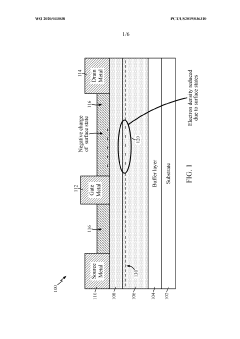
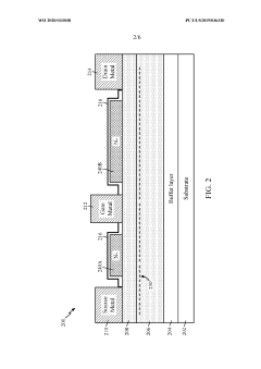
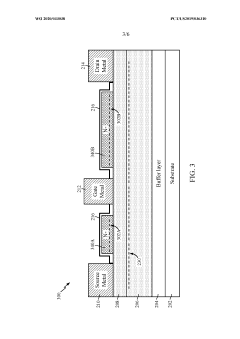
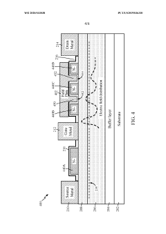
Gallium nitride high electron mobility transistor with ledges and field plates
PatentWO2020033038A1
Innovation
- Incorporating n-doped protuberances, or ledges, between the gate and source/drain electrodes, and optionally using field plates, to reduce surface states and increase channel electron density, thereby enhancing breakdown voltage and switching efficiency.
Reliability Assessment Frameworks for GaN HEMTs
Reliability assessment frameworks for GaN HEMTs have evolved significantly to address the unique challenges posed by these high-power devices. The industry has developed comprehensive methodologies that combine accelerated life testing, statistical analysis, and physics-of-failure approaches to accurately predict device lifetime and performance degradation under various operational conditions.
The JEDEC standards, particularly JEP122 and JEP148, provide foundational frameworks for reliability assessment of semiconductor devices, which have been adapted specifically for GaN HEMT evaluation. These frameworks typically incorporate multiple stress tests including High Temperature Operating Life (HTOL), High Temperature Reverse Bias (HTRB), and Temperature Humidity Bias (THB) tests to simulate extreme operating conditions.
Time-Dependent Dielectric Breakdown (TDDB) assessment has emerged as a critical component in GaN HEMT reliability frameworks, especially for high-voltage applications where gate dielectric integrity is paramount. Modern frameworks incorporate specialized TDDB models that account for the unique material properties and failure mechanisms of GaN devices.
Mean Time To Failure (MTTF) prediction methodologies have been refined for GaN technology, with Arrhenius-based models being supplemented by more sophisticated approaches that account for multiple failure mechanisms occurring simultaneously. These frameworks now commonly employ Weibull statistical distributions to characterize failure rates and project device lifetimes under normal operating conditions.
Electro-thermal reliability assessment has gained prominence in GaN HEMT frameworks, recognizing the critical interplay between electrical performance and thermal management in high-power applications. Advanced frameworks now incorporate coupled electro-thermal simulation tools that can predict hotspot formation and progressive degradation under dynamic operating conditions.
Mission-profile based reliability assessment represents the cutting edge of GaN HEMT evaluation, where actual application conditions are simulated to provide more realistic lifetime predictions. These frameworks translate laboratory test results to field reliability by accounting for the specific power cycling, temperature fluctuations, and electrical stresses encountered in target applications such as power conversion systems or RF amplifiers.
Standardized reporting metrics have been established within these frameworks to facilitate comparison between different GaN technologies and manufacturers. Key reliability indicators now commonly include activation energies for various degradation mechanisms, voltage acceleration factors, and statistical confidence intervals for lifetime predictions.
Thermal Management Considerations in Testing
Thermal management represents a critical aspect of GaN HEMT testing for high-power applications, as these devices generate significant heat during operation that can dramatically affect performance and reliability. When designing test setups for GaN HEMTs, engineers must implement comprehensive thermal control strategies to ensure accurate characterization and prevent device degradation or failure.
Temperature monitoring forms the foundation of effective thermal management during testing. Advanced infrared thermal imaging systems provide real-time temperature distribution maps across the device surface, while integrated temperature sensors enable precise monitoring at critical points. These monitoring systems must be calibrated specifically for GaN materials, as their thermal emission properties differ from traditional semiconductors.
Heat dissipation mechanisms require careful consideration in test fixture design. Custom heat sinks with optimized fin structures and materials with superior thermal conductivity (such as diamond-copper composites) have demonstrated significant improvements in testing accuracy. Liquid cooling systems utilizing dielectric fluids have emerged as particularly effective for high-power density testing scenarios, allowing for stable device temperatures even under extreme power conditions.
The thermal resistance path from junction to case represents a key parameter requiring accurate measurement during testing. Transient thermal impedance measurement techniques have been developed specifically for GaN HEMTs, enabling the characterization of thermal bottlenecks within the device structure. This data proves invaluable for both device optimization and reliability prediction.
Pulsed testing protocols have become standard practice for high-power GaN HEMT evaluation, allowing devices to be characterized under realistic operating conditions while minimizing self-heating effects. Pulse width and duty cycle optimization requires careful consideration of the device's thermal time constants, which can be extracted through specialized measurement techniques.
Environmental chamber integration with test systems enables performance evaluation across the intended operating temperature range, from cryogenic to elevated temperatures exceeding 200°C. These chambers must maintain precise temperature control while accommodating the necessary RF and DC connections for comprehensive device characterization.
Thermal simulation tools have evolved to address the unique challenges of GaN HEMT testing, incorporating accurate models of thermal boundary resistances and material properties specific to GaN device structures. These simulations guide test fixture design and help establish safe operating limits during testing procedures, preventing thermal runaway conditions that could damage devices or testing equipment.
Unlock deeper insights with PatSnap Eureka Quick Research — get a full tech report to explore trends and direct your research. Try now!
Generate Your Research Report Instantly with AI Agent
Supercharge your innovation with PatSnap Eureka AI Agent Platform!