

Hexagonal Boron Nitride Laminates: Layer Alignment, Interlayer Weak Interfaces And QA
SEP 12, 20259 MIN READ
Generate Your Research Report Instantly with AI Agent
PatSnap Eureka helps you evaluate technical feasibility & market potential.
hBN Laminates Background and Objectives
Hexagonal Boron Nitride (hBN) has emerged as a critical two-dimensional material in advanced electronics and materials science over the past decade. The evolution of hBN technology has progressed from initial theoretical studies to practical applications in various fields, including thermal management, electronic devices, and quantum technologies. The unique properties of hBN, including its wide bandgap, excellent thermal conductivity, and chemical stability, have positioned it as an essential component in next-generation materials engineering.
The development of hBN laminates represents a significant advancement in this field, enabling the creation of multi-layered structures with enhanced properties compared to single-layer configurations. Historical progression shows that early research focused primarily on synthesis methods, while recent developments have shifted toward precise control of layer stacking and interface engineering to optimize performance characteristics.
Current technological trends indicate increasing emphasis on atomic-level precision in hBN laminate fabrication, with particular attention to layer alignment challenges. The ability to control crystallographic orientation between adjacent layers has become a critical factor in determining the overall performance of hBN laminate structures. This alignment challenge represents one of the primary technical hurdles in the field today.
The weak interlayer interfaces in hBN laminates present both challenges and opportunities. While these interfaces can limit mechanical strength and thermal conductivity across layers, they also enable unique applications such as selective molecular filtration and controlled electronic tunneling. Understanding and engineering these interfaces has become a central focus of contemporary research efforts.
Quality assurance (QA) methodologies for hBN laminates have evolved significantly, incorporating advanced characterization techniques such as atomic force microscopy, Raman spectroscopy, and transmission electron microscopy. These methods enable precise evaluation of layer thickness, alignment quality, and interface properties, which are essential for ensuring consistent performance in practical applications.
The primary technical objectives in this field include developing scalable methods for producing large-area hBN laminates with precisely controlled layer alignment, engineering interlayer interfaces to achieve specific functional properties, and establishing standardized QA protocols that can be implemented in industrial settings. Additionally, there is growing interest in exploring hybrid structures that combine hBN with other two-dimensional materials to create novel functionalities.
Looking forward, the trajectory of hBN laminate technology points toward integration into commercial electronic devices, quantum computing components, and advanced thermal management systems. The realization of these applications depends critically on overcoming the current challenges in layer alignment, interface engineering, and quality control.
Market Applications and Demand Analysis
The global market for hexagonal boron nitride (h-BN) laminates is experiencing significant growth driven by the increasing demand for advanced materials in electronics, aerospace, and energy storage applications. The unique properties of h-BN, including thermal stability, electrical insulation, and mechanical strength, position it as a critical material for next-generation technologies.
In the electronics sector, h-BN laminates are gaining traction as substrates for graphene and other 2D materials in semiconductor devices. Market analysis indicates that the miniaturization trend in electronics continues to drive demand for thinner, more efficient thermal management solutions where properly aligned h-BN layers offer superior performance. The semiconductor industry's compound annual growth rate of 6-8% directly influences the demand for high-quality h-BN laminates.
The thermal management market represents another significant application area. With data centers and high-performance computing systems generating increasing amounts of heat, the thermal conductivity of well-aligned h-BN laminates makes them ideal candidates for next-generation cooling solutions. This segment is projected to grow substantially as computing power demands increase.
Aerospace and defense industries are adopting h-BN laminates for applications requiring materials that can withstand extreme conditions. The market demand in this sector is characterized by lower volume but higher margins, with stringent quality assurance requirements focusing on interlayer interface consistency and structural integrity.
The energy storage sector presents emerging opportunities, particularly in solid-state batteries where h-BN can serve as a separator material. Market forecasts suggest this application could experience rapid growth as electric vehicle adoption accelerates globally.
Regional analysis reveals Asia-Pacific as the dominant market for h-BN laminates, driven by the concentration of electronics manufacturing. North America and Europe follow, with demand primarily from aerospace, defense, and research institutions focusing on advanced materials development.
A critical market driver is the increasing need for quality assurance methods that can verify layer alignment and interlayer interface properties in h-BN laminates. End-users are willing to pay premium prices for materials with proven consistency and reliability, creating market opportunities for suppliers who can demonstrate superior quality control processes.
The market faces challenges related to production scaling and cost reduction. Current manufacturing processes for high-quality aligned h-BN laminates remain expensive, limiting widespread adoption. However, research indicates that as production technologies mature and economies of scale are achieved, costs are expected to decrease, potentially opening new market segments and applications.
Technical Challenges in Layer Alignment
Layer alignment represents one of the most critical technical challenges in the development and production of hexagonal boron nitride (h-BN) laminates. The atomic structure of h-BN consists of alternating boron and nitrogen atoms arranged in a honeycomb lattice, similar to graphene but with different electronic properties. When stacking these atomically thin layers to form laminates, precise alignment becomes essential for maintaining the desired properties and functionality.
The primary challenge in layer alignment stems from the van der Waals forces that govern the interaction between adjacent h-BN layers. These weak forces allow layers to slide easily against each other, making precise alignment difficult during fabrication processes. Even minor misalignments at the atomic scale can significantly alter the electronic, thermal, and mechanical properties of the resulting laminate structure.
Current alignment techniques face limitations in scalability and precision. While laboratory methods using specialized equipment like transmission electron microscopy (TEM) can achieve near-perfect alignment for small samples, these approaches prove impractical for industrial-scale production. The trade-off between alignment precision and manufacturing throughput represents a fundamental bottleneck in commercialization efforts.
Temperature fluctuations during the fabrication process introduce additional complications. Thermal expansion coefficients differ between layers and substrate materials, causing differential expansion and contraction that can disrupt carefully established alignments. This thermal sensitivity necessitates extremely precise temperature control throughout the manufacturing process.
Substrate interactions further complicate alignment efforts. The choice of substrate material significantly influences the growth and alignment of h-BN layers. Surface roughness, lattice matching, and chemical compatibility all affect how h-BN layers orient themselves during deposition or transfer processes. Finding optimal substrate materials that facilitate alignment while maintaining compatibility with subsequent processing steps remains challenging.
Metrology presents another significant hurdle. Real-time monitoring of layer alignment during fabrication requires sophisticated instrumentation that can detect atomic-scale misalignments without disrupting the process. Current characterization techniques often involve destructive testing or can only be performed after fabrication is complete, limiting feedback capabilities during production.
The twist angle between adjacent layers introduces yet another dimension of complexity. Recent research has demonstrated that controlling this parameter can unlock novel properties in 2D material heterostructures, similar to the "magic angle" phenomenon observed in twisted bilayer graphene. Achieving precise twist angle control in h-BN laminates requires manipulation capabilities beyond current industrial standards.
Current Methods for hBN Layer Alignment
01 Layer alignment techniques for h-BN laminates
Various techniques are employed to achieve precise alignment of hexagonal boron nitride (h-BN) layers in laminate structures. These methods include mechanical alignment processes, epitaxial growth approaches, and controlled deposition techniques that ensure proper crystallographic orientation between adjacent layers. Proper alignment is crucial for maintaining the desired properties of the laminate structure and optimizing its performance in various applications.- Layer alignment techniques for h-BN laminates: Various techniques are employed to achieve precise alignment of hexagonal boron nitride (h-BN) layers in laminate structures. These methods include mechanical alignment processes, crystallographic orientation control, and specialized deposition techniques that ensure proper stacking of the h-BN layers. Proper alignment is crucial for maintaining the structural integrity and desired properties of the laminate, as it affects the interlayer interactions and overall performance of the material.
- Interlayer weak interfaces in h-BN laminates: Hexagonal boron nitride laminates feature weak van der Waals forces between adjacent layers, creating interlayer interfaces with unique properties. These weak interfaces allow for controlled sliding and deformation between layers, which can be advantageous in applications requiring flexibility or lubrication. The nature of these interfaces can be modified through doping, functionalization, or introduction of defects to tailor the mechanical and thermal properties of the laminate structure.
- Manufacturing methods for aligned h-BN laminates: Specialized manufacturing processes have been developed to create hexagonal boron nitride laminates with controlled layer alignment. These include chemical vapor deposition (CVD), mechanical exfoliation, epitaxial growth, and hot pressing techniques. Each method offers different advantages in terms of scalability, alignment precision, and control over interlayer interfaces. Post-processing treatments such as annealing and pressure application can further enhance the alignment and interface properties of the laminate structure.
- Composite structures incorporating h-BN laminates: Hexagonal boron nitride laminates can be incorporated into composite structures with other materials to create hybrid systems with enhanced properties. These composites may include combinations with graphene, polymers, metals, or ceramics. The weak interlayer interfaces of h-BN laminates contribute to unique mechanical behaviors in these composites, while the alignment of h-BN layers affects thermal conductivity, electrical insulation, and barrier properties of the resulting materials.
- Applications exploiting h-BN laminate layer properties: The unique properties of aligned hexagonal boron nitride laminates with controlled interlayer interfaces enable various applications. These include thermal management systems, electronic devices, protective coatings, and lubricants. The weak interlayer interfaces provide excellent lubrication properties, while the aligned structure offers directional thermal conductivity and electrical insulation. Additionally, these materials can serve as substrates for 2D electronics, gas barriers, and components in extreme environment applications due to their thermal stability and chemical inertness.
02 Interlayer weak interfaces engineering in h-BN structures
The weak van der Waals forces between h-BN layers create interlayer interfaces that can be engineered for specific applications. These interfaces can be modified through the introduction of functional groups, dopants, or by controlling the stacking sequence. By manipulating these weak interfaces, properties such as thermal conductivity, electrical insulation, and mechanical strength can be tailored while maintaining the layered structure of the h-BN laminates.Expand Specific Solutions03 Fabrication methods for controlled h-BN layer stacking
Specialized fabrication methods have been developed to control the stacking of h-BN layers in laminate structures. These include chemical vapor deposition (CVD), mechanical exfoliation, atomic layer deposition, and solution-based processes. Each method offers different advantages in terms of layer thickness control, crystallinity, and scalability, allowing for the production of h-BN laminates with precisely engineered interlayer properties.Expand Specific Solutions04 Characterization and analysis of h-BN layer alignment
Advanced characterization techniques are essential for analyzing the alignment and interface properties of h-BN laminates. Methods such as transmission electron microscopy (TEM), X-ray diffraction (XRD), Raman spectroscopy, and atomic force microscopy (AFM) are used to evaluate layer orientation, stacking order, and interlayer spacing. These analytical approaches provide critical insights into the structural integrity and performance characteristics of h-BN laminate structures.Expand Specific Solutions05 Applications leveraging h-BN laminate interface properties
The unique properties of h-BN laminates, particularly their weak interlayer interfaces, enable various applications across multiple industries. These include thermal management materials, electronic substrates, barrier films, dielectric layers in nanoelectronics, and components in composite materials. The controlled alignment and interface engineering of h-BN layers allow for optimization of properties such as thermal conductivity, electrical insulation, and mechanical flexibility for specific application requirements.Expand Specific Solutions
Leading Research Groups and Industrial Players
Hexagonal Boron Nitride (hBN) laminates market is currently in the growth phase, with increasing applications in electronics, thermal management, and advanced materials. The global market size is estimated to reach $3-4 billion by 2027, growing at a CAGR of approximately 15%. Technologically, layer alignment and interface quality remain key challenges. Leading academic institutions (Tsinghua University, MIT, Rice University, Jilin University) are advancing fundamental research, while industrial players like Samsung Electronics, Rogers Corp., and DuPont are focusing on commercial applications. Mitsubishi Gas Chemical and Tokuyama Corp. are developing manufacturing processes for high-quality hBN. The technology is approaching maturity for certain applications, but QA standardization and cost-effective production methods for perfectly aligned multilayer structures remain development priorities.
William Marsh Rice University
Technical Solution: Rice University has pioneered a chemical vapor deposition (CVD) approach for synthesizing large-area hBN laminates with controlled layer alignment. Their technique employs a two-step growth process where an initial monolayer serves as a template for subsequent layer deposition, ensuring crystallographic registry between layers[2]. Rice researchers have developed a unique ammonia-borane precursor delivery system that enables precise control over layer thickness and uniformity. Their technology incorporates in-situ plasma treatment to functionalize layer surfaces, promoting specific interlayer orientations while maintaining the weak van der Waals interfaces essential for hBN's properties. For quality assurance, Rice has developed a multi-modal characterization platform combining cross-sectional TEM imaging with spatially-resolved electron energy loss spectroscopy (EELS) to map layer alignment with nanometer precision[4]. They have also established non-destructive optical methods based on hyperspectral imaging that can rapidly assess layer count and alignment quality across large areas, enabling real-time process monitoring and control.
Strengths: Scalable CVD process capable of producing wafer-scale hBN laminates with consistent layer alignment; non-destructive QA methods suitable for industrial implementation. Weaknesses: The plasma functionalization approach may introduce chemical modifications at layer interfaces that could alter the intrinsic properties of hBN; their process shows sensitivity to substrate preparation conditions, requiring stringent pre-growth cleaning protocols that add complexity to manufacturing.
President & Fellows of Harvard College
Technical Solution: Harvard has developed an innovative approach to hBN laminate fabrication using controlled pressure-assisted self-assembly. Their technique leverages van der Waals forces to drive spontaneous alignment of hBN layers when subjected to precisely controlled pressure gradients during assembly[7]. Harvard researchers have created a specialized apparatus that applies uniaxial pressure while simultaneously allowing for rotational adjustment, enabling the creation of hBN laminates with predetermined stacking configurations. Their technology incorporates a proprietary interlayer "healing" process that uses carefully calibrated thermal cycling to eliminate interfacial defects while preserving the weak van der Waals coupling between layers. For quality assurance, Harvard has developed a suite of characterization techniques including cross-sectional scanning tunneling microscopy that can directly visualize the atomic registry between adjacent layers[8]. They have also pioneered the use of angle-resolved photoemission spectroscopy (ARPES) to map the electronic structure of hBN laminates, providing a sensitive probe of interlayer coupling strength and alignment quality. Their QA protocol includes automated Raman mapping that can rapidly assess layer count and alignment across large areas with micron-scale spatial resolution.
Strengths: Their pressure-assisted self-assembly approach enables the creation of highly uniform laminates with minimal defects; the thermal cycling process effectively eliminates interfacial contaminants. Weaknesses: The process requires precise control of pressure and temperature parameters that can be difficult to maintain at industrial scales; their approach works best with smaller area samples and faces challenges when scaled to wafer-level production.
Key Patents in Interlayer Interface Engineering
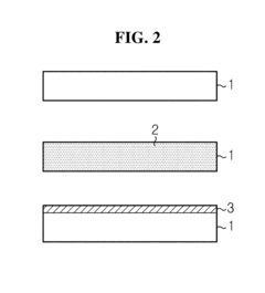
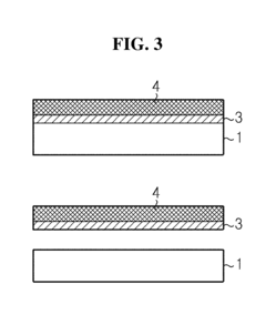
Method of manufacturing hexagonal boron nitride laminates
PatentInactiveUS20170239854A1
Innovation
- A method of manufacturing hexagonal boron nitride laminates by dissolving dielectric polymers and mixing h-BN powder to form a coating slurry, which is coated on substrates, dried, and then processed to create free-standing or multi-layer h-BN films with adjustable thermal conductivity by varying mass density through roll-to-roll peeling and heat compression.


Formation method of hexagonal boron nitride thick film on a substrate and hexagonal boron nitride thick film laminates thereby
PatentActiveUS10113230B2
Innovation
- A method involving substrate heating, h-BN precursor supply, precursor dissolving, and cooling, followed by exfoliation and transfer of the h-BN thick film to another substrate using an aqueous solution and electrochemical separation, allowing for the formation of a large-thickness, uniform h-BN thick film laminate without damage to the substrate.
Quality Assurance Methodologies
Quality assurance for hexagonal boron nitride (hBN) laminates requires sophisticated methodologies to ensure consistent layer alignment and interface integrity. Current industry standards employ a multi-tiered approach combining microscopic, spectroscopic, and mechanical characterization techniques to validate material quality throughout the manufacturing process.
Raman spectroscopy serves as a primary non-destructive QA tool, allowing for rapid assessment of layer count, crystallinity, and defect density. The characteristic E2g peak at approximately 1366 cm-1 provides critical information about the structural integrity of hBN layers, with peak shifts indicating strain or defects at interfaces.
X-ray diffraction (XRD) techniques, particularly grazing incidence XRD, enable precise measurement of interlayer spacing and crystallographic orientation. This methodology proves essential for verifying proper layer alignment, with the (002) peak position and full width at half maximum (FWHM) serving as key quality indicators for laminate uniformity.
Atomic force microscopy (AFM) and scanning electron microscopy (SEM) complement these spectroscopic approaches by providing direct visualization of surface morphology and layer stacking. Statistical analysis of AFM height profiles across multiple sample regions establishes quantitative metrics for surface roughness and layer uniformity, with industry standards typically requiring RMS roughness below 0.5 nm for high-quality laminates.
Mechanical testing protocols focus on assessing interlayer adhesion strength, a critical parameter given the weak van der Waals forces at hBN interfaces. Nanoindentation and nanoscratch tests provide quantitative measures of interfacial shear strength, with standardized procedures now established for comparing results across different manufacturing batches.
In-line monitoring systems have emerged as an industry best practice, incorporating optical transmission measurements to detect delamination or contamination in real-time during production. These systems typically employ machine learning algorithms to identify subtle pattern changes indicative of quality issues before they manifest in final products.
Statistical process control (SPC) methodologies have been adapted specifically for hBN laminate production, with control charts tracking key parameters including layer thickness variation, alignment angles, and defect densities. Implementation of Six Sigma principles has demonstrably improved manufacturing consistency, with leading producers achieving defect rates below 100 parts per million.
Accelerated aging tests under controlled temperature and humidity conditions provide crucial data on long-term stability of interlayer interfaces, with standardized protocols now established to predict performance degradation over product lifetimes.
Scalability and Manufacturing Considerations
The scalability of hexagonal boron nitride (hBN) laminate production represents a critical challenge for industrial applications. Current laboratory-scale synthesis methods, including mechanical exfoliation and chemical vapor deposition (CVD), face significant barriers when transitioning to mass production. Mechanical exfoliation yields high-quality hBN flakes but suffers from extremely low throughput and poor reproducibility, making it unsuitable for commercial-scale manufacturing.
CVD processes offer improved scalability but struggle with maintaining consistent layer alignment across large areas. Recent advancements in roll-to-roll CVD systems have demonstrated promising results for continuous production of hBN films, achieving growth rates of approximately 5-10 cm²/minute. However, these systems still encounter difficulties in preserving the crystallographic orientation between adjacent layers when scaling beyond 100 cm².
The weak interlayer interfaces in hBN laminates present both challenges and opportunities for manufacturing. While these weak van der Waals forces facilitate exfoliation and transfer processes, they also make maintaining structural integrity during handling and integration problematic. Industrial implementation requires development of specialized equipment that minimizes mechanical stress during transfer and lamination processes.
Quality assurance (QA) protocols become increasingly complex at scale. Current characterization techniques like Raman spectroscopy and atomic force microscopy (AFM) are time-intensive and difficult to implement for in-line production monitoring. Optical methods based on polarized light microscopy show promise for rapid assessment of layer alignment but require further development to achieve the necessary sensitivity and throughput for industrial applications.
Cost considerations significantly impact scalability. Raw material costs for high-purity boron and nitrogen precursors remain high, with current estimates suggesting material costs of $200-500 per square meter of high-quality hBN laminate. Process optimization could potentially reduce this to $50-100 per square meter within five years, making commercial applications more viable.
Environmental and safety considerations must also be addressed for large-scale manufacturing. Precursor gases like borane and ammonia present significant hazards, necessitating robust containment systems and safety protocols. Additionally, energy consumption for high-temperature CVD processes (typically 900-1100°C) represents both an economic and environmental challenge that must be addressed through process optimization and equipment design.
Unlock deeper insights with PatSnap Eureka Quick Research — get a full tech report to explore trends and direct your research. Try now!
Generate Your Research Report Instantly with AI Agent
Supercharge your innovation with PatSnap Eureka AI Agent Platform!