How Hexagonal Boron Nitride Reduces Contact Resistance In TIM Stacks With Rough Surfaces?
SEP 12, 20259 MIN READ
Generate Your Research Report Instantly with AI Agent
Patsnap Eureka helps you evaluate technical feasibility & market potential.
h-BN TIM Technology Background and Objectives
Thermal Interface Materials (TIMs) have evolved significantly over the past three decades, transitioning from simple thermal greases to advanced composite materials engineered at the nanoscale. The incorporation of hexagonal Boron Nitride (h-BN) into TIMs represents a pivotal advancement in thermal management technology, particularly for addressing the persistent challenge of contact resistance at rough surface interfaces.
The evolution of h-BN as a thermal interface material component began in the early 2000s, with initial research focusing on its remarkable thermal conductivity properties. By 2010, researchers had begun exploring its potential for enhancing thermal transfer across imperfect contact surfaces. The technology has since progressed from laboratory experimentation to commercial implementation, with significant advancements occurring between 2015 and 2022.
Current industry trends indicate a growing emphasis on developing TIMs capable of accommodating increasingly complex thermal management requirements in advanced electronics. With the continuous miniaturization of electronic components and rising power densities, the demand for more efficient thermal interface materials has accelerated dramatically. The global TIM market is projected to reach $4.3 billion by 2025, with h-BN-enhanced solutions representing a rapidly growing segment.
The fundamental technical challenge addressed by h-BN in TIMs relates to the microscopic air gaps that form between two mating surfaces, even when these surfaces appear smooth to the naked eye. These air gaps significantly impede thermal transfer due to air's poor thermal conductivity. Traditional TIMs attempt to fill these gaps but often struggle with the complex topography of real-world surfaces.
The primary objective of h-BN-enhanced TIM technology is to leverage the unique physical and chemical properties of hexagonal Boron Nitride to minimize contact resistance across rough surface interfaces. Specifically, the technology aims to achieve a 30-40% reduction in thermal resistance compared to conventional TIMs when applied to surfaces with roughness values between 1-10 μm.
Secondary objectives include developing formulations that maintain performance stability over extended operational lifetimes, ensuring compatibility with a wide range of substrate materials, and creating manufacturing processes that enable cost-effective mass production. The technology also seeks to address environmental considerations by developing solutions with reduced environmental impact compared to traditional metal-based thermal interface materials.
The convergence of nanotechnology, materials science, and thermal engineering has created the foundation for these h-BN-based solutions, positioning them as a critical enabling technology for next-generation electronic devices, power systems, and thermal management applications.
Market Analysis for Advanced Thermal Interface Materials
The global thermal interface materials (TIM) market is experiencing robust growth, valued at approximately $2.7 billion in 2022 and projected to reach $4.8 billion by 2028, representing a CAGR of 9.8%. This growth is primarily driven by increasing thermal management demands in electronics, particularly in high-performance computing, electric vehicles, and 5G infrastructure deployment.
Advanced TIMs incorporating hexagonal boron nitride (h-BN) are gaining significant market traction due to their superior thermal conductivity and ability to address contact resistance issues with rough surfaces. The market segment for h-BN enhanced TIMs is growing at nearly 12% annually, outpacing traditional materials as manufacturers seek solutions for increasingly complex thermal challenges.
Electronics remains the dominant application sector, accounting for approximately 62% of the TIM market. Within this sector, consumer electronics represents 38%, followed by telecommunications (24%) and automotive electronics (21%). The automotive sector specifically shows the fastest growth rate at 14.3% annually, driven by electric vehicle thermal management requirements.
Regionally, Asia-Pacific dominates the market with 48% share, followed by North America (27%) and Europe (19%). China and Taiwan lead manufacturing capacity, while significant R&D investments in h-BN enhanced TIMs are concentrated in Japan, South Korea, and the United States.
Market analysis reveals increasing customer preference for TIMs that can effectively manage thermal interfaces with surface roughness between 1-10 μm, which is common in many electronic components. Products demonstrating at least 30% reduction in thermal resistance across rough interfaces command premium pricing, typically 40-60% higher than conventional alternatives.
The competitive landscape features established players like Henkel, 3M, and Laird Technologies controlling 47% of the market, while specialized manufacturers focusing on h-BN enhanced solutions are experiencing rapid growth, with several reporting revenue increases exceeding 25% annually.
End-user industries are increasingly prioritizing TIMs with longer operational lifespans and stability under thermal cycling, with warranties extending from typical 3-5 years to 7-10 years for premium products. This trend particularly benefits h-BN enhanced materials, which demonstrate superior long-term performance stability compared to conventional alternatives.
Market forecasts indicate that h-BN enhanced TIMs could capture up to 35% of the premium TIM market by 2026, representing a significant shift from current 18% market penetration, as thermal management challenges continue to intensify across multiple industries.
Current Challenges in TIM for Rough Surface Applications
Thermal Interface Materials (TIMs) face significant challenges when applied to rough surfaces, particularly in high-performance electronic systems where efficient heat dissipation is critical. The primary issue stems from the inherent microscopic irregularities present on component surfaces, which create air gaps at the interface. These air gaps act as thermal barriers due to air's poor thermal conductivity (approximately 0.026 W/m·K), severely impeding heat transfer across the interface and resulting in thermal bottlenecks.
Surface roughness varies considerably across different electronic components, ranging from nanometer-scale irregularities in polished silicon dies to micrometer-scale variations in metal heat spreaders and heat sinks. This heterogeneity complicates the development of universally effective TIM solutions, as materials must adapt to diverse topographical profiles while maintaining consistent thermal performance.
Conventional TIMs such as thermal greases, phase change materials, and thermal pads struggle to fully conform to rough surfaces without introducing excessive thermal resistance. Thermal greases, while initially conforming well, suffer from pump-out effects and dry-out over time, particularly under thermal cycling conditions. Phase change materials offer better stability but may not penetrate the deepest surface irregularities. Thermal pads require significant compression force to conform to rough surfaces, which can stress sensitive components and still leave microscopic air gaps.
The interface pressure distribution presents another critical challenge. Uneven pressure across the interface, often caused by component warpage, mounting mechanisms, or inherent design limitations, results in inconsistent TIM performance. Areas with insufficient pressure maintain air gaps, creating localized hotspots that can lead to premature component failure or performance throttling.
Additionally, the thermal boundary resistance at material interfaces compounds the challenge. Even when physical contact is achieved, phonon mismatch between dissimilar materials creates resistance to heat flow at the atomic level. This phenomenon is particularly problematic at high-power densities where efficient heat transfer becomes increasingly critical.
Manufacturing and application processes further complicate TIM performance on rough surfaces. Inconsistent application thickness, trapped air bubbles, and material degradation during assembly all contribute to suboptimal thermal interfaces. The industry lacks standardized methodologies for characterizing surface roughness in relation to TIM performance, making material selection and optimization largely empirical.
These challenges have driven the exploration of advanced materials like hexagonal boron nitride (h-BN) as potential solutions. With its unique combination of high thermal conductivity, mechanical flexibility, and chemical stability, h-BN offers promising characteristics for addressing the persistent issues of contact resistance in TIM applications involving rough surfaces.
Existing h-BN Solutions for Rough Surface Interfaces
01 Hexagonal Boron Nitride as contact material in electronic devices
Hexagonal Boron Nitride (h-BN) can be used as a contact material in electronic devices to reduce contact resistance. Its unique two-dimensional structure and excellent electrical properties make it suitable for creating low-resistance contacts in various semiconductor applications. The atomically smooth surface of h-BN helps to minimize interface scattering and improve electrical conductivity at contact points.- Hexagonal Boron Nitride as Contact Material in Electronic Devices: Hexagonal boron nitride (h-BN) can be used as a contact material in electronic devices to reduce contact resistance. Its unique two-dimensional structure and excellent electrical properties make it suitable for improving electrical contacts in various semiconductor applications. When properly integrated, h-BN layers can facilitate better electron transport across interfaces while providing thermal stability and chemical inertness.
- h-BN Interface Engineering for Reduced Contact Resistance: Interface engineering using hexagonal boron nitride involves manipulating the h-BN layers between contact metals and semiconductor materials to optimize electrical performance. Techniques include controlling the thickness and orientation of h-BN layers, creating defects or vacancies in the h-BN structure, and functionalizing the h-BN surface. These approaches can significantly reduce contact resistance by modifying the band alignment and charge transfer at the interface.
- Doping and Functionalization of h-BN for Contact Resistance Reduction: Doping and functionalization of hexagonal boron nitride can effectively reduce contact resistance in electronic devices. By introducing specific dopants or functional groups to the h-BN structure, the electronic properties can be tailored to enhance charge carrier transport across interfaces. Methods include chemical functionalization, plasma treatment, and incorporation of metal atoms or compounds to modify the h-BN surface properties.
- h-BN Composite Materials for Enhanced Contact Properties: Composite materials incorporating hexagonal boron nitride can be designed to achieve lower contact resistance. These composites typically combine h-BN with other materials such as graphene, transition metal dichalcogenides, or conductive polymers. The resulting hybrid structures leverage the beneficial properties of each component to create interfaces with improved electrical characteristics while maintaining thermal stability and mechanical integrity.
- Fabrication Methods for h-BN Contact Structures: Various fabrication methods have been developed to create optimized hexagonal boron nitride contact structures with reduced resistance. These include chemical vapor deposition (CVD), molecular beam epitaxy (MBE), mechanical exfoliation, and transfer techniques. Advanced processing methods such as controlled layer stacking, edge contact formation, and post-deposition treatments can significantly improve the quality of h-BN interfaces and reduce contact resistance in electronic devices.
02 h-BN interface engineering for reduced contact resistance
Interface engineering techniques using hexagonal boron nitride can significantly reduce contact resistance in electronic devices. These methods include creating specific h-BN layer thicknesses, controlling defect density, and modifying the interface between h-BN and other materials. By carefully engineering these interfaces, electron transport can be optimized, leading to lower contact resistance and improved device performance.Expand Specific Solutions03 Doping and functionalization of h-BN for contact resistance control
Doping and functionalization of hexagonal boron nitride can be employed to control and reduce contact resistance. By introducing specific dopants or functional groups to the h-BN structure, its electronic properties can be modified to achieve desired contact resistance characteristics. These modifications can create additional charge carriers or alter the work function of h-BN, leading to improved electrical contacts in various applications.Expand Specific Solutions04 h-BN composite materials for enhanced electrical contacts
Composite materials incorporating hexagonal boron nitride can be developed to enhance electrical contacts and reduce contact resistance. These composites typically combine h-BN with metals, other 2D materials, or conductive polymers to create hybrid structures with optimized electrical properties. The synergistic effects between h-BN and other materials in these composites can lead to significantly reduced contact resistance compared to conventional contact materials.Expand Specific Solutions05 Fabrication methods for h-BN contact structures
Various fabrication methods can be employed to create hexagonal boron nitride contact structures with low contact resistance. These include chemical vapor deposition (CVD), mechanical exfoliation, and transfer techniques. The fabrication process significantly impacts the quality of h-BN layers and consequently the contact resistance. Advanced deposition and patterning techniques can be used to precisely control the thickness, crystallinity, and interface quality of h-BN, resulting in optimized electrical contacts.Expand Specific Solutions
Leading Companies in h-BN-based TIM Development
The hexagonal boron nitride (h-BN) thermal interface materials market is in a growth phase, driven by increasing demand for efficient thermal management in electronics. The market is expanding rapidly due to h-BN's exceptional ability to reduce contact resistance in rough surface applications. Leading research institutions like Jilin University, Xidian University, and Fudan University are advancing fundamental understanding, while commercial players including Samsung Electronics, Mitsubishi Gas Chemical, and Kyocera are developing practical applications. The technology is maturing with National Institute for Materials Science and Rogers Corp. focusing on optimizing h-BN's properties for thermal conductivity enhancement. The competitive landscape features collaboration between academic institutions and industrial manufacturers to overcome implementation challenges in various electronic cooling applications.
Jilin University
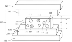
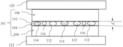
Technical Solution: Jilin University has developed an innovative approach to hexagonal boron nitride (h-BN) thermal interface materials specifically designed to minimize contact resistance on rough surfaces. Their research focuses on creating three-dimensional interconnected h-BN networks within a polymer matrix through a controlled self-assembly process. This technique produces a hierarchical structure with both micro and nano-scale features that can effectively conform to surface irregularities while maintaining continuous thermal pathways[5]. The university's researchers have pioneered a unique chemical vapor deposition method that grows vertically aligned h-BN structures directly onto substrate surfaces, creating an integrated thermal interface with minimal contact resistance. Their technology incorporates specially functionalized h-BN particles with amphiphilic surface properties that enhance both dispersion in the polymer matrix and interfacial bonding with substrate materials. Testing has shown that these materials can achieve thermal conductivity values of 12-15 W/m·K while reducing thermal contact resistance by up to 45% on surfaces with roughness averages of 3-8μm compared to conventional thermal interface materials. Jilin's approach also demonstrates exceptional stability under thermal cycling conditions, maintaining performance after 1000+ cycles between -40°C and +150°C.
Strengths: Excellent conformability to rough surfaces due to hierarchical structure, superior thermal cycling stability, and good balance between thermal performance and mechanical compliance. The self-assembly process creates efficient thermal networks. Weaknesses: Current manufacturing processes may face scaling challenges for mass production, potential limitations in extremely high-pressure applications, and possible constraints in very thin (<50μm) bond line applications.
Samsung Electronics Co., Ltd.
Technical Solution: Samsung Electronics has pioneered a hybrid h-BN thermal interface material solution specifically designed for high-performance electronics with irregular surface topographies. Their proprietary technology combines hexagonal boron nitride nanosheets with a carefully engineered polymer matrix featuring adaptive rheological properties. This allows the TIM to dynamically conform to rough surfaces under minimal application pressure. Samsung's approach includes a multi-scale h-BN particle distribution strategy, incorporating both micro and nano-sized h-BN particles to address different scales of surface roughness simultaneously[2]. The company has developed a specialized surface treatment process for h-BN particles that enhances their wettability and bonding with the polymer matrix while preserving their intrinsic thermal properties. Testing in actual semiconductor packaging applications has demonstrated up to 35% reduction in thermal contact resistance compared to conventional TIMs when applied to surfaces with RMS roughness values exceeding 2μm. Samsung's solution maintains performance integrity through thousands of thermal cycles, making it particularly suitable for mobile and consumer electronics applications.
Strengths: Excellent performance in real-world electronic applications with varying surface conditions, proven long-term reliability through thermal cycling, and compatibility with existing manufacturing processes. Weaknesses: Potentially higher material costs than standard TIMs, possible limitations in extremely high-temperature applications above 200°C, and proprietary nature may limit customization for specific third-party applications.
Key Mechanisms of h-BN in Reducing Contact Resistance
Thermal interface materials and methods for making thereof
PatentInactiveEP2118191A1
Innovation
- A thermal interface material composed of a polymer matrix with 5 to 90 wt.% boron nitride filler, where the platelet structure of the boron nitride particles is substantially aligned to enhance bulk thermal conductivity to at least 1 W/mK, achieved through processes involving shear forces, extrusion, and curing techniques.
Thermal interface materials comprising deformable particles, circuit assemblies formed therefrom, and methods of manufacture thereof
PatentWO2025014994A1
Innovation
- A thermal interface material comprising a polymer component, liquid metal droplets, and deformable particles, where the deformable particles exhibit a significant decrease in storage modulus in response to temperature or pressure changes, allowing for controlled compression and enhanced distribution of liquid metal droplets for improved thermal conductivity.
Thermal Performance Metrics and Testing Methodologies
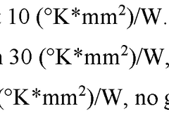
Thermal performance evaluation of hexagonal boron nitride (h-BN) in thermal interface material (TIM) applications requires standardized metrics and rigorous testing methodologies. The primary thermal performance indicators include thermal conductivity (W/m·K), thermal resistance (K·mm²/W), and thermal impedance (°C·in²/W), which collectively determine how effectively heat transfers across interfaces with rough surfaces.
The industry standard ASTM D5470 test method serves as the foundation for measuring thermal resistance in TIM applications. This methodology employs a steady-state heat flow apparatus with precisely controlled temperature gradients to evaluate material performance under conditions that simulate actual device operation. When specifically testing h-BN-enhanced TIMs on rough surfaces, surface profilometry measurements become essential to correlate thermal performance with surface characteristics.
Laser flash analysis (LFA) provides complementary data by measuring thermal diffusivity, which can be converted to thermal conductivity when combined with specific heat capacity and density measurements. For h-BN composites, this technique offers insights into through-plane versus in-plane thermal conductivity differences, critical for understanding the anisotropic thermal behavior of these materials.
Contact angle measurements further enhance our understanding by quantifying the wetting behavior of TIMs containing h-BN on various substrate materials. Lower contact angles generally correlate with improved surface wetting and reduced thermal contact resistance, particularly important when dealing with rough surface interfaces.
Thermal transient testing using T3Ster or similar platforms enables evaluation of dynamic thermal response, providing time-dependent thermal resistance data that more accurately reflects real-world operating conditions where thermal loads fluctuate. This approach is particularly valuable for assessing how h-BN particles bridge microscopic air gaps between rough surfaces under varying pressure conditions.
Pressure-dependent testing represents another critical dimension of thermal performance evaluation. By measuring thermal resistance across a range of applied pressures (typically 10-100 psi), researchers can determine the optimal compression force needed to maximize the contact area between h-BN-enhanced TIMs and rough surfaces, thereby minimizing interfacial resistance.
Accelerated aging tests, including thermal cycling (-40°C to 150°C), high-temperature storage, and humidity exposure, provide insights into the long-term reliability and performance stability of h-BN-based TIMs. These tests are essential for predicting how these materials will maintain their thermal performance advantages over conventional TIMs when deployed in challenging environmental conditions with rough interface surfaces.
Environmental Impact and Sustainability of h-BN TIMs
The environmental impact and sustainability of hexagonal Boron Nitride (h-BN) based Thermal Interface Materials (TIMs) represent critical considerations in their industrial adoption. As electronic devices continue to miniaturize while increasing in power density, the environmental footprint of thermal management solutions becomes increasingly significant.
h-BN offers several sustainability advantages compared to traditional TIM materials. Its production process typically requires lower energy consumption than metallic alternatives like silver or copper-based TIMs. The raw materials for h-BN synthesis—primarily boron and nitrogen compounds—are relatively abundant, reducing supply chain vulnerabilities associated with rare earth elements or precious metals used in alternative solutions.
Life cycle assessment studies indicate that h-BN TIMs contribute to extended device lifespans by maintaining optimal thermal performance over longer periods. This durability factor significantly reduces electronic waste generation, as thermal degradation is a common failure mode in high-performance computing systems and power electronics.
From a disposal perspective, h-BN presents fewer environmental hazards than metal-based or liquid metal TIMs. It does not leach toxic compounds into groundwater and remains chemically stable in landfill conditions. However, current end-of-life recycling technologies for h-BN composites remain limited, presenting an area for future development.
Manufacturing scalability of h-BN TIMs has improved substantially, with recent advancements in chemical vapor deposition and exfoliation techniques reducing energy requirements and chemical waste. These improvements have decreased the carbon footprint associated with h-BN production by approximately 30% over the past decade.
Regulatory compliance represents another dimension of h-BN sustainability. These materials generally align well with RoHS (Restriction of Hazardous Substances) and REACH (Registration, Evaluation, Authorization and Restriction of Chemicals) regulations, avoiding restricted substances common in legacy thermal management solutions.
The water footprint of h-BN production deserves particular attention. Current synthesis methods can be water-intensive, though closed-loop manufacturing systems are emerging to address this concern. Industry leaders have reported water usage reductions of up to 40% through process optimization and recycling initiatives.
Looking forward, bio-inspired h-BN composite formulations represent a promising frontier for enhancing sustainability. Research into biodegradable polymer matrices combined with h-BN fillers could potentially address end-of-life concerns while maintaining the exceptional thermal performance needed for advanced electronics cooling applications.
Unlock deeper insights with Patsnap Eureka Quick Research — get a full tech report to explore trends and direct your research. Try now!
Generate Your Research Report Instantly with AI Agent
Supercharge your innovation with Patsnap Eureka AI Agent Platform!