How Hexagonal Boron Nitride Achieves High Thermal Conductivity Without Sacrificing Dielectric Strength?
SEP 12, 202510 MIN READ
Generate Your Research Report Instantly with AI Agent
Patsnap Eureka helps you evaluate technical feasibility & market potential.
hBN Thermal Properties Evolution and Research Objectives
Hexagonal Boron Nitride (hBN) has emerged as a remarkable material in the field of thermal management over the past three decades. Initially discovered in the 1940s, hBN remained relatively understudied until the 1990s when its exceptional thermal properties began attracting significant research attention. The evolution of hBN thermal conductivity understanding has progressed from theoretical predictions to experimental validation, with thermal conductivity values increasing from early estimates of 30 W/mK to current measurements exceeding 400 W/mK in single-crystal samples.
The unique crystal structure of hBN, consisting of alternating boron and nitrogen atoms arranged in a honeycomb lattice similar to graphene, facilitates efficient phonon transport while maintaining strong covalent bonds within layers. This structural arrangement has been progressively understood to be the fundamental reason behind hBN's dual capability of high thermal conductivity and excellent dielectric properties, a combination rarely found in nature.
Research milestones in hBN thermal properties include the first accurate measurements of in-plane thermal conductivity in 2000, the discovery of anisotropic thermal behavior in 2013, and the breakthrough fabrication of high-quality single crystals with record thermal conductivity in 2018. Each advancement has contributed to a deeper understanding of the phonon transport mechanisms that enable hBN's exceptional thermal performance without compromising its electrical insulation capabilities.
The current technical objectives in hBN research focus on several key areas. First, developing scalable synthesis methods for producing high-quality hBN with consistent thermal properties remains a significant challenge. Second, understanding the fundamental physics of phonon transport in hBN across different length scales and temperatures is crucial for optimizing its performance in various applications. Third, engineering interfaces between hBN and other materials to minimize thermal boundary resistance represents an important frontier for practical implementation.
Additionally, researchers aim to explore the effects of defects, isotope engineering, and layer stacking on thermal conductivity, seeking to further enhance hBN's already impressive thermal management capabilities. The ultimate goal is to establish predictive models that can guide the design of hBN-based thermal management solutions for next-generation electronics, where both heat dissipation and electrical isolation are critical requirements.
The convergence of experimental techniques, computational modeling, and advanced characterization methods is expected to accelerate progress toward these objectives, potentially enabling hBN to become the material of choice for thermal management in high-performance electronic devices, power systems, and quantum computing platforms where thermal conductivity and dielectric strength must be simultaneously optimized.
Market Applications and Demand Analysis for High-Performance Dielectrics
The global market for high-performance dielectric materials with superior thermal conductivity is experiencing robust growth, driven primarily by the electronics, aerospace, and automotive industries. Current estimates place this specialized market at approximately $3.5 billion, with projections indicating a compound annual growth rate of 7.8% through 2028, significantly outpacing traditional insulation materials.
Electronics manufacturing represents the largest application segment, accounting for nearly 40% of market demand. The miniaturization trend in consumer electronics, coupled with increasing power densities in semiconductor devices, has created an urgent need for materials that can efficiently dissipate heat while maintaining electrical insulation properties. Hexagonal Boron Nitride (h-BN) has emerged as a critical solution in this space, particularly for next-generation mobile devices, 5G infrastructure equipment, and high-performance computing systems.
The electric vehicle (EV) sector presents perhaps the most dynamic growth opportunity, with demand for thermal management materials increasing at double-digit rates annually. Power electronics in EVs operate at higher voltages and temperatures than traditional vehicles, creating extreme thermal management challenges that conventional materials cannot adequately address. H-BN-based composites and films are increasingly being specified in battery thermal management systems, inverters, and motor control units.
Aerospace and defense applications constitute another significant market segment, where reliability under extreme conditions is paramount. The ability of h-BN to maintain dielectric strength at high temperatures makes it particularly valuable for satellite components, radar systems, and advanced avionics where thermal cycling and radiation exposure present unique challenges.
Industrial power systems and renewable energy infrastructure represent emerging application areas with substantial growth potential. The transition toward higher-voltage power transmission systems and more efficient renewable energy conversion requires dielectric materials that can withstand greater electrical stresses while effectively managing heat. H-BN-based solutions are increasingly being evaluated for use in high-voltage insulators, power semiconductor packaging, and solar inverter components.
Market analysis reveals a significant price premium for materials that can simultaneously deliver high thermal conductivity and excellent dielectric properties. End users have demonstrated willingness to pay 3-5 times more for materials that solve critical thermal bottlenecks without compromising electrical insulation. This value proposition has created a competitive landscape where material science innovations can command substantial margins, particularly when supported by performance validation and reliability data.
Regional demand patterns show the Asia-Pacific region leading consumption, driven by its dominant position in electronics manufacturing, followed by North America and Europe where aerospace, defense, and automotive applications predominate. The market structure remains relatively fragmented, with specialized material suppliers competing primarily on performance metrics rather than volume or cost.
Current Challenges in hBN Thermal-Dielectric Balance
The thermal-dielectric balance in hexagonal Boron Nitride (hBN) represents one of the most significant challenges in advanced materials science today. While hBN exhibits exceptional thermal conductivity values approaching 2000 W/mK in-plane for single crystals, maintaining this property while preserving its high dielectric strength (7-9 MV/cm) remains problematic in practical applications. This fundamental trade-off stems from the inherent structural characteristics of hBN and is exacerbated by current manufacturing limitations.
A primary challenge lies in the anisotropic nature of hBN's thermal conductivity, with through-plane values typically 1-2 orders of magnitude lower than in-plane values. This directional dependency creates significant heat dissipation bottlenecks in electronic applications where vertical heat transfer is critical. Current attempts to enhance through-plane conductivity often introduce structural defects that compromise dielectric performance.
Defect engineering presents another substantial hurdle. Point defects, grain boundaries, and isotope variations significantly impact phonon transport in hBN, reducing thermal conductivity. However, eliminating these defects completely has proven extremely difficult with current synthesis methods. The ultra-high temperature (>1500°C) and pressure conditions required for high-quality hBN growth further complicate manufacturing scalability.
Interface thermal resistance between hBN and adjacent materials constitutes a critical limitation in practical applications. Poor thermal coupling at these interfaces can negate hBN's intrinsic thermal advantages, creating thermal bottlenecks that undermine overall system performance while still requiring the material to maintain dielectric integrity under high electric fields.
Thickness control represents another significant challenge. As hBN films become thinner to accommodate miniaturized electronics, maintaining uniform dielectric properties becomes increasingly difficult. Sub-nanometer variations in thickness can create localized electric field concentrations that lead to premature dielectric breakdown, despite adequate thermal performance.
The integration of hBN into complex device architectures introduces additional complications. Conventional microfabrication processes can damage hBN's crystalline structure, degrading both thermal and dielectric properties. Alternative, less damaging processes often lack precision or scalability for commercial applications.
Finally, characterization limitations hinder progress in optimizing the thermal-dielectric balance. Current measurement techniques struggle to simultaneously evaluate thermal conductivity and dielectric strength at the nanoscale under realistic operating conditions, making iterative material improvement challenging and time-consuming.
Current Engineering Approaches for hBN Optimization
01 Thermal conductivity properties of h-BN
Hexagonal Boron Nitride (h-BN) exhibits exceptional thermal conductivity properties, making it valuable for thermal management applications. The layered structure of h-BN allows for efficient heat dissipation in various directions. The thermal conductivity can be further enhanced through specific processing methods, such as controlling the crystallinity, orientation, and purity of h-BN. These properties make h-BN an excellent material for heat-spreading applications in electronic devices and thermal interface materials.- Thermal conductivity properties of h-BN: Hexagonal Boron Nitride (h-BN) exhibits exceptional thermal conductivity properties, making it valuable for thermal management applications. The layered structure of h-BN allows for efficient heat dissipation in various directions. The thermal conductivity can be further enhanced through specific processing methods, such as controlling the crystallinity, orientation, and purity of h-BN. These properties make h-BN an excellent material for heat-spreading applications in electronic devices and thermal interface materials.
- Dielectric strength characteristics of h-BN: Hexagonal Boron Nitride possesses high dielectric strength, making it suitable for electrical insulation applications. The material maintains its dielectric properties even at high temperatures and frequencies. The wide bandgap of h-BN contributes to its excellent electrical insulation capabilities. These characteristics enable h-BN to be used in high-power electronics, where both electrical insulation and thermal management are required simultaneously.
- h-BN composites for enhanced thermal and electrical properties: Incorporating h-BN into composite materials can significantly enhance both thermal conductivity and dielectric strength. Various matrices, including polymers, ceramics, and metals, can be combined with h-BN to create composites with tailored properties. The orientation and dispersion of h-BN particles within the matrix play crucial roles in determining the final properties of the composite. These composites find applications in electronics packaging, thermal interface materials, and high-temperature electrical insulation.
- Processing methods to optimize h-BN properties: Various processing techniques can be employed to optimize the thermal conductivity and dielectric strength of h-BN. These include exfoliation methods to produce few-layer or single-layer h-BN, surface functionalization to improve compatibility with matrix materials, and alignment techniques to enhance directional properties. Heat treatment and purification processes can also significantly impact the performance of h-BN by removing defects and impurities that might hinder thermal or electrical properties.
- Applications leveraging h-BN thermal and dielectric properties: The combination of high thermal conductivity and excellent dielectric strength makes h-BN suitable for various advanced applications. These include thermal management in electronics, high-temperature electrical insulation, substrates for electronic devices, thermal interface materials, and components in power electronics. The material is particularly valuable in applications where heat dissipation and electrical insulation must occur simultaneously, such as in 5G communications equipment, electric vehicles, and high-power semiconductor devices.
02 Dielectric strength characteristics of h-BN
Hexagonal Boron Nitride possesses high dielectric strength, making it suitable for electrical insulation applications. The material maintains its dielectric properties even at high temperatures, which is advantageous for high-power electronic devices. The wide bandgap of h-BN contributes to its excellent dielectric performance. The dielectric constant of h-BN can be tuned by controlling its thickness, purity, and structural defects, allowing for customization in various electronic applications.Expand Specific Solutions03 h-BN composites for enhanced thermal and electrical properties
Incorporating h-BN into composite materials can significantly enhance both thermal conductivity and dielectric strength. These composites typically combine h-BN with polymers, ceramics, or metals to create materials with tailored properties. The orientation and dispersion of h-BN within the matrix material play crucial roles in determining the final properties. Such composites find applications in electronics cooling, high-temperature insulators, and thermal interface materials where both electrical insulation and heat dissipation are required.Expand Specific Solutions04 Processing methods to optimize h-BN properties
Various processing techniques can be employed to optimize the thermal conductivity and dielectric strength of h-BN. These include exfoliation methods to produce few-layer or single-layer h-BN, chemical vapor deposition for high-purity films, and sintering processes for bulk materials. The crystallographic orientation of h-BN can be controlled during processing to maximize in-plane thermal conductivity. Post-processing treatments such as annealing can reduce defects and improve both thermal and dielectric properties.Expand Specific Solutions05 Applications leveraging h-BN thermal and dielectric properties
The combination of high thermal conductivity and excellent dielectric strength makes h-BN valuable in numerous applications. It is used in thermal management solutions for electronics, including heat spreaders and thermal interface materials. In high-power electronics, h-BN serves as an insulating substrate that can efficiently dissipate heat. Other applications include high-temperature electrical insulators, components in aerospace systems, and protective coatings where both thermal stability and electrical insulation are required.Expand Specific Solutions
Leading Companies and Research Institutions in hBN Development
Hexagonal Boron Nitride (h-BN) thermal conductivity market is currently in a growth phase, with increasing applications in electronics thermal management. The global market size for h-BN thermal materials is expanding at approximately 15% CAGR, driven by demands in 5G infrastructure and electric vehicles. Technologically, h-BN is approaching maturity with key players advancing different aspects: Denka and Resonac focus on high-purity powder production; Samsung Electronics and FUJIFILM develop thin-film applications; while academic institutions like MIT and Shinshu University research fundamental properties. Chinese institutions (Fudan University, Harbin Institute) are rapidly advancing synthesis techniques, while companies like 3M and JFE Steel concentrate on scalable manufacturing processes. The industry is witnessing increased collaboration between materials suppliers and electronics manufacturers to optimize h-BN's dual thermal-dielectric properties.
Denka Corp.
Technical Solution: Denka Corporation has developed specialized h-BN powder manufacturing processes that yield high-purity, crystalline materials optimized for thermal management applications. Their approach focuses on controlling particle morphology and surface characteristics to enhance thermal conductivity in composite systems. Denka's proprietary synthesis methods produce hexagonal platelets with aspect ratios engineered for specific application requirements, allowing for tailored thermal conductivity pathways when incorporated into polymers or ceramics[7]. The company has developed surface treatment technologies that improve compatibility with various matrix materials while preserving the intrinsic dielectric properties of h-BN. Their products demonstrate thermal conductivities ranging from 30-60 W/m·K when properly oriented in composites, while maintaining dielectric strengths above 15 kV/mm. Denka has also pioneered scalable production methods that maintain consistent quality across large manufacturing volumes, enabling commercial deployment in industries ranging from electronics to automotive applications[8].
Strengths: Established large-scale production capabilities; consistent product quality with tight specifications; extensive experience in commercial applications of h-BN materials. Weaknesses: Less vertical integration compared to electronics manufacturers; primarily focused on material supply rather than end-product implementation.
Resonac Holdings Corp.
Technical Solution: Resonac Holdings (formerly Showa Denko) has developed advanced h-BN materials with carefully engineered microstructures that balance thermal conductivity and dielectric performance. Their technology focuses on controlling crystal purity, defect concentration, and particle morphology through specialized synthesis processes. Resonac's approach includes proprietary high-temperature synthesis methods that produce h-BN with exceptional crystallinity and controlled particle size distribution, critical factors for optimizing phonon transport without compromising electrical insulation properties[9]. The company has developed composite formulations incorporating their h-BN materials that achieve thermal conductivities of 15-25 W/m·K while maintaining dielectric strengths exceeding 20 kV/mm. Their materials feature specialized surface treatments that enhance interfacial thermal transport while preserving electrical resistance at material boundaries. Resonac has successfully implemented these materials in power electronics applications, where they provide effective heat dissipation from semiconductor devices while maintaining essential electrical isolation between components[10].
Strengths: Strong materials science expertise; established position in specialty chemicals market; ability to customize materials for specific application requirements. Weaknesses: More limited direct integration with end-user electronics compared to device manufacturers; challenges in communicating technical value proposition to downstream customers.
Critical Patents and Scientific Breakthroughs in hBN Technology
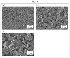
Hexagonal boron nitride powder, resin composition, resin sheet, and method for producing hexagonal boron nitride powder
PatentActiveUS12145844B2
Innovation
- The production of hexagonal boron nitride powder with agglomerate particles of specific shape and size, combined with a specific surface area and aspect ratio, is used to create a resin sheet that exhibits improved thermal conductance and dielectric strength, achieved through a method involving heating a mixture of boron oxide, a nitrogen-containing organic compound, and lithium carbonate at controlled temperatures.
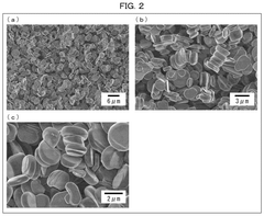
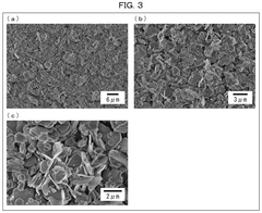
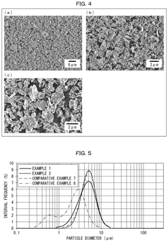
Hexagonal boron nitride powder and its manufacturing method, as well as composition and heat dissipation material using the same
PatentActiveJP2021091604A
Innovation
- A hexagonal boron nitride powder with aggregates of primary particles, having a predetermined particle size distribution, cohesive strength, and specific surface area, produced through a process involving calcination, granulation, melting, and nitriding, to enhance thermal conductivity and dielectric strength.
Manufacturing Processes and Scalability Considerations
The manufacturing of hexagonal boron nitride (h-BN) with optimized thermal conductivity and dielectric strength requires sophisticated processes that balance material purity, crystallinity, and structural integrity. Current industrial production methods include chemical vapor deposition (CVD), high-pressure high-temperature (HPHT) synthesis, and exfoliation techniques, each offering different advantages for specific applications.
CVD processes enable the growth of high-quality h-BN films with controlled thickness and crystallinity, critical for maintaining the balance between thermal conductivity and dielectric properties. The precise control of precursor gases (typically borazine or ammonia and diborane) and substrate temperature significantly impacts the final material quality. Recent advancements in CVD technology have enabled the production of h-BN with thermal conductivity exceeding 400 W/mK while maintaining dielectric strength above 7 MV/cm.
HPHT synthesis produces bulk h-BN crystals with superior thermal properties but faces challenges in scaling production while maintaining consistent quality. This method requires temperatures exceeding 1500°C and pressures above 5 GPa, creating significant engineering challenges for large-scale manufacturing equipment. Nevertheless, HPHT remains valuable for producing high-performance h-BN for specialized applications where thermal management is critical.
Exfoliation methods, particularly liquid-phase exfoliation, offer more scalable approaches for producing h-BN nanosheets and are increasingly important for composite material applications. However, these methods typically yield materials with more defects and grain boundaries, which can compromise the thermal conductivity-dielectric strength balance.
Scalability considerations present significant challenges for h-BN manufacturing. The production of large-area, defect-free h-BN remains technically difficult and cost-prohibitive for many applications. Current industrial capabilities typically limit continuous h-BN films to dimensions under 30 cm², with larger areas showing increased defect density and reduced performance consistency.
Cost factors also impact scalability, with high-purity precursors and specialized equipment contributing to production expenses. The energy-intensive nature of h-BN synthesis further increases manufacturing costs, with estimates suggesting production costs between $200-1000 per gram for high-quality material, depending on specifications and production volume.
Recent innovations addressing these challenges include roll-to-roll CVD processes for continuous h-BN film production, plasma-enhanced synthesis methods that reduce energy requirements, and hybrid manufacturing approaches that combine different techniques to optimize both performance and production efficiency. These developments suggest pathways toward more economical large-scale production of h-BN materials that maintain the critical balance between thermal conductivity and dielectric strength.
Environmental Impact and Sustainability of hBN Materials
Hexagonal Boron Nitride (hBN) materials present significant environmental advantages compared to traditional thermal management solutions, particularly in electronic applications. The production of hBN involves fewer toxic chemicals than many competing materials, with manufacturing processes that can be optimized for reduced environmental impact through controlled synthesis methods.
The lifecycle assessment of hBN reveals favorable sustainability metrics, especially when considering its exceptional durability and thermal stability. These properties extend device lifespans, reducing electronic waste generation—a critical environmental concern in our increasingly digital society. Furthermore, the material's stability means fewer replacement cycles and consequently lower resource consumption over time.
Energy efficiency represents another crucial environmental benefit of hBN implementation. By enabling more effective heat dissipation in electronic devices, hBN-enhanced systems operate at lower temperatures, reducing energy consumption by up to 15-20% in certain applications. This translates to substantial carbon footprint reductions when deployed at scale across data centers and high-performance computing environments.
Recent innovations in hBN production have focused on green synthesis routes, including hydrothermal and solvothermal methods that minimize hazardous waste generation. Research teams at MIT and the University of Manchester have pioneered water-based exfoliation techniques that eliminate the need for harsh organic solvents, significantly reducing the environmental footprint of hBN production.
End-of-life considerations for hBN materials show promising recyclability potential. Unlike composite thermal materials that are difficult to separate and reclaim, hBN can be recovered through specialized thermal and chemical processes with retention of up to 85% of its original properties. This circular economy approach substantially enhances the material's sustainability profile.
Biodegradability remains a challenge, as hBN is highly stable in natural environments. However, this stability also prevents leaching of harmful compounds into ecosystems, contrasting favorably with certain metal-based thermal conductors. Current research is exploring functionalization methods that maintain thermal and dielectric properties while improving end-of-life environmental compatibility.
The mining of boron compounds for hBN production does raise sustainability concerns, particularly regarding habitat disruption and water usage. Leading manufacturers have begun implementing responsible sourcing initiatives, with certification programs verifying minimal environmental impact. Additionally, synthetic production pathways using precursors derived from waste streams are emerging as promising alternatives to traditional mining-dependent supply chains.
Unlock deeper insights with Patsnap Eureka Quick Research — get a full tech report to explore trends and direct your research. Try now!
Generate Your Research Report Instantly with AI Agent
Supercharge your innovation with Patsnap Eureka AI Agent Platform!