How Boron Nitride Substrates Balance Thermal Conductivity With Mechanical Robustness?
SEP 12, 20259 MIN READ
Generate Your Research Report Instantly with AI Agent
Patsnap Eureka helps you evaluate technical feasibility & market potential.
BN Substrate Technology Evolution and Objectives
Boron Nitride (BN) substrates have emerged as a critical material in advanced electronics and thermal management systems over the past three decades. The evolution of BN substrate technology began in the early 1990s with rudimentary forms primarily used in specialized laboratory applications. Initially, these substrates faced significant limitations in both manufacturing scalability and performance consistency, restricting their commercial viability.
By the early 2000s, advancements in chemical vapor deposition (CVD) and hot pressing techniques revolutionized BN substrate production, enabling the creation of more uniform and larger-scale substrates. This period marked the transition from purely experimental applications to early industrial adoption, particularly in high-temperature electronics and specialized semiconductor packaging.
The fundamental challenge that has driven BN substrate development is the inherent trade-off between thermal conductivity and mechanical robustness. Pure hexagonal boron nitride (h-BN) exhibits exceptional thermal conductivity along its basal planes (up to 2000 W/m·K), rivaling or exceeding many metals, while maintaining electrical insulation properties. However, this same crystalline structure that enables superior thermal performance also creates planes of weakness that compromise mechanical integrity.
Recent technological evolution has focused on composite approaches and novel manufacturing techniques to overcome this fundamental limitation. Between 2010 and 2020, significant breakthroughs occurred in creating BN composites that incorporate secondary phases or structural modifications to enhance mechanical properties without severely compromising thermal performance.
The current technological objective centers on achieving an optimal balance between these competing properties. Specifically, researchers and industry leaders aim to develop BN substrates with thermal conductivity exceeding 1000 W/m·K while simultaneously achieving flexural strength above 300 MPa and fracture toughness greater than 5 MPa·m^(1/2). These targets represent a 30-40% improvement over current commercial offerings.
Looking forward, the technology roadmap for BN substrates includes several ambitious objectives: developing scalable manufacturing processes for complex BN architectures, creating gradient-functional BN substrates with region-specific properties, and establishing comprehensive modeling frameworks that accurately predict performance under various thermal and mechanical stress conditions.
The ultimate goal is to position BN substrates as the material of choice for next-generation thermal management solutions in applications ranging from high-power electronics and 5G/6G infrastructure to aerospace systems and electric vehicle power modules, where the balance between thermal efficiency and mechanical reliability is paramount for system performance and longevity.
Market Analysis for High-Performance Thermal Management Materials
The thermal management materials market is experiencing robust growth, driven by increasing demands from electronics, aerospace, automotive, and energy sectors. The global market for high-performance thermal management materials was valued at approximately 11.3 billion USD in 2022 and is projected to reach 18.7 billion USD by 2028, representing a compound annual growth rate of 8.7%. This growth trajectory is particularly significant for advanced materials like boron nitride substrates, which occupy a specialized segment within this expanding market.
Consumer electronics remains the largest application segment, accounting for nearly 35% of the market share. The miniaturization trend in electronic devices, coupled with increasing power densities, has intensified the need for efficient thermal management solutions. Boron nitride substrates, with their exceptional thermal conductivity and electrical insulation properties, are increasingly being adopted in high-end electronic applications where traditional materials fail to meet performance requirements.
The automotive sector represents another significant growth area, particularly with the rapid expansion of electric vehicles (EVs). The thermal management systems market for EVs alone is expected to grow at a CAGR of 12.6% through 2030. Boron nitride substrates are finding applications in power electronics, battery thermal management systems, and LED lighting in automotive applications, where their combination of thermal conductivity and mechanical robustness provides critical performance advantages.
Regionally, Asia-Pacific dominates the market with approximately 42% share, followed by North America and Europe. China, Japan, South Korea, and Taiwan are key manufacturing hubs driving demand for advanced thermal management materials, including boron nitride substrates. The concentration of semiconductor and electronics manufacturing in these regions creates substantial market opportunities.
A notable market trend is the increasing preference for materials that offer multifunctional properties. Boron nitride substrates are well-positioned in this regard, as they balance excellent thermal conductivity with mechanical robustness, chemical stability, and electrical insulation. This combination addresses multiple engineering challenges simultaneously, providing significant value proposition for manufacturers.
Price sensitivity remains a market constraint, particularly for hexagonal boron nitride (h-BN) substrates, which involve complex manufacturing processes. However, as production technologies mature and economies of scale improve, price points are expected to become more competitive, potentially expanding market penetration across various industries.
The market is also witnessing increased research and development investments, with a focus on enhancing the performance-to-cost ratio of boron nitride-based materials. This R&D emphasis is likely to yield more cost-effective manufacturing methods and hybrid materials that optimize the balance between thermal conductivity and mechanical properties.
Current Challenges in BN Substrate Development
Despite significant advancements in boron nitride (BN) substrate technology, several critical challenges persist in achieving the optimal balance between thermal conductivity and mechanical robustness. The primary obstacle lies in the manufacturing process, where producing high-quality, defect-free hexagonal boron nitride (h-BN) at scale remains difficult. Current synthesis methods, including chemical vapor deposition (CVD) and high-pressure high-temperature (HPHT) techniques, often introduce structural imperfections that compromise both thermal performance and mechanical integrity.
Material purity represents another significant challenge, as even trace impurities can dramatically reduce thermal conductivity while creating potential fracture points. The industry standard currently struggles to consistently achieve purity levels above 99.9%, with the remaining contaminants often clustering at grain boundaries and creating thermal bottlenecks.
Grain boundary engineering presents a complex trade-off scenario. While smaller grain sizes generally enhance mechanical strength through crack deflection mechanisms, they simultaneously reduce thermal conductivity by increasing phonon scattering. Conversely, larger crystalline domains improve heat transfer but may compromise structural integrity under mechanical stress.
Thickness uniformity across large-area substrates remains problematic, with variations often exceeding ±10% in commercial products. These inconsistencies create unpredictable thermal gradients and mechanical stress concentrations that can lead to premature failure in high-performance applications.
Interface engineering between BN substrates and adjacent materials presents another significant hurdle. Poor adhesion can create thermal contact resistance that negates the inherent conductivity advantages of BN, while excessive bonding strength may transfer external mechanical stresses directly to the BN substrate, increasing fracture risk.
Cost-effectiveness continues to limit widespread adoption, with high-quality BN substrates commanding prices 5-10 times higher than conventional alternatives. This economic barrier restricts BN implementation primarily to high-value applications where performance justifies the premium.
Environmental stability under extreme operating conditions remains inadequate for certain applications. While BN demonstrates excellent thermal stability, its susceptibility to oxidation above 850°C in air and potential degradation in certain chemical environments limits its application range. Additionally, cyclic thermal loading can induce cumulative damage that progressively reduces both thermal conductivity and mechanical strength over time.
Characterization and quality control methodologies lack standardization across the industry, making it difficult to reliably compare products from different manufacturers or predict in-service performance based on laboratory measurements. This uncertainty increases development cycles and implementation risks for end-users.
Existing Approaches to Balance Thermal-Mechanical Properties
01 Hexagonal Boron Nitride (h-BN) for High Thermal Conductivity
Hexagonal boron nitride (h-BN) substrates exhibit exceptional thermal conductivity properties, making them ideal for heat dissipation applications in electronic devices. The crystalline structure of h-BN allows for efficient phonon transport, resulting in thermal conductivity values that can exceed 2000 W/mK in-plane. These substrates can be synthesized through various methods including chemical vapor deposition (CVD) and high-temperature high-pressure techniques to achieve optimal thermal performance while maintaining structural integrity.- Hexagonal Boron Nitride (h-BN) for High Thermal Conductivity: Hexagonal boron nitride (h-BN) substrates exhibit exceptional thermal conductivity properties, making them ideal for heat dissipation applications in electronic devices. The crystalline structure of h-BN allows for efficient phonon transport, resulting in thermal conductivity values that can exceed 2000 W/mK in-plane. These substrates can be synthesized through various methods including chemical vapor deposition (CVD) and high-temperature, high-pressure techniques to optimize their thermal performance while maintaining structural integrity.
- Mechanical Robustness Enhancement Techniques: Various techniques have been developed to enhance the mechanical robustness of boron nitride substrates. These include the incorporation of reinforcing materials such as carbon fibers, ceramic particles, or polymer matrices to create composite structures. Surface treatments and specialized coating processes can also improve the fracture toughness and flexural strength of BN substrates. Additionally, controlled grain size and orientation during fabrication significantly impact the mechanical properties, with nano-structured BN showing superior mechanical performance compared to conventional forms.
- Boron Nitride Composite Substrates: Composite substrates incorporating boron nitride with other materials offer a balance between thermal conductivity and mechanical strength. By combining BN with materials such as aluminum nitride, silicon carbide, or various polymers, these composites can be tailored for specific applications. The synergistic effects between BN and complementary materials allow for enhanced thermal management while maintaining or improving mechanical properties. These composites are particularly valuable in applications requiring both heat dissipation and structural integrity under mechanical stress.
- Thin Film and 2D Boron Nitride Structures: Thin film and two-dimensional boron nitride structures offer unique thermal and mechanical properties for specialized applications. These ultra-thin BN layers can be grown with precise control over thickness and crystal orientation, resulting in exceptional in-plane thermal conductivity while maintaining flexibility. The 2D nature of these structures allows for integration into flexible electronics and thermal interface materials. Various deposition techniques including molecular beam epitaxy and chemical vapor deposition enable the fabrication of these advanced BN structures with tailored properties.
- Processing Methods for Optimized BN Substrate Properties: Specialized processing methods have been developed to optimize both the thermal conductivity and mechanical robustness of boron nitride substrates. These include hot pressing, spark plasma sintering, and pressure-assisted sintering techniques that control the microstructure and density of the material. Post-processing treatments such as annealing and surface functionalization can further enhance thermal interfaces and mechanical strength. The processing parameters significantly influence the crystallinity, grain boundaries, and defect concentration, which directly impact the thermal and mechanical performance of the final BN substrate.
02 Mechanical Strength Enhancement Techniques for BN Substrates
Various techniques have been developed to enhance the mechanical robustness of boron nitride substrates. These include the incorporation of reinforcing materials such as carbon fibers, ceramic particles, or polymer matrices to create composite structures. Surface treatments and specialized sintering processes can also improve the fracture toughness and flexural strength of BN substrates. The mechanical properties can be further optimized through controlled grain size distribution and the elimination of structural defects during the manufacturing process.Expand Specific Solutions03 Cubic Boron Nitride (c-BN) for Extreme Conditions
Cubic boron nitride (c-BN) substrates offer superior hardness and thermal stability under extreme conditions. With a structure similar to diamond, c-BN provides exceptional mechanical robustness while maintaining good thermal conductivity. These substrates are particularly valuable in high-temperature and high-pressure applications where both thermal management and structural integrity are critical. The synthesis of c-BN typically involves specialized high-pressure high-temperature (HPHT) techniques to achieve the desired cubic crystal structure.Expand Specific Solutions04 Thin Film and 2D BN for Flexible Electronics
Thin film and two-dimensional boron nitride substrates offer unique combinations of flexibility and thermal conductivity for next-generation electronics. These ultra-thin BN structures can be integrated into flexible and wearable devices while providing effective heat dissipation pathways. The atomically thin nature of 2D BN allows for conformal integration with curved surfaces while maintaining impressive in-plane thermal conductivity. Various deposition and transfer techniques have been developed to create these thin BN substrates with minimal defects.Expand Specific Solutions05 BN Composite Substrates for Tailored Properties
Boron nitride composite substrates combine the thermal conductivity of BN with complementary properties from other materials to achieve tailored performance characteristics. By incorporating materials such as aluminum nitride, silicon carbide, or various metals, these composites can offer optimized combinations of thermal conductivity, mechanical strength, and electrical insulation. The composition and microstructure can be engineered to meet specific application requirements, from high-power electronics to aerospace components. Advanced manufacturing techniques including spark plasma sintering and hot pressing enable precise control over the final properties.Expand Specific Solutions
Leading Manufacturers and Research Institutions in BN Industry
The boron nitride substrate market is in a growth phase, characterized by increasing demand for thermal management solutions in electronics and aerospace applications. The market size is expanding due to the rising need for materials that can balance thermal conductivity with mechanical robustness. From a technological maturity perspective, established players like Momentive Performance Materials, Denka Corp., and FUJIFILM Corp. are leading commercial development, while research institutions such as National Institute for Materials Science and Nanyang Technological University are advancing fundamental innovations. Companies including Teijin Ltd., Sekisui Chemical, and Rogers Corp. are developing specialized applications in high-performance materials. The competitive landscape shows a mix of chemical conglomerates and specialized materials manufacturers working to optimize the thermal-mechanical balance that makes boron nitride substrates increasingly valuable for next-generation electronics.
National Institute for Materials Science IAI
Technical Solution: NIMS has pioneered innovative approaches to h-BN substrate development through their advanced materials engineering program. Their research focuses on controlling the crystallographic orientation of h-BN layers to maximize in-plane thermal conductivity while enhancing cross-plane mechanical strength. NIMS researchers have developed a pressure-assisted sintering technique that creates highly oriented h-BN structures with thermal conductivity reaching 120 W/m·K along preferred directions while maintaining fracture toughness above 3 MPa·m^1/2. Their nano-engineered interfaces incorporate secondary phase reinforcements at grain boundaries, creating mechanical interlocking structures that prevent crack propagation without compromising thermal pathways. NIMS has also developed composite h-BN substrates with gradient porosity structures that optimize the balance between thermal performance and mechanical resilience, particularly for applications requiring thermal cycling resistance.
Strengths: Exceptional thermal conductivity (up to 120 W/m·K) through crystallographic orientation control; superior fracture toughness compared to conventional h-BN; innovative gradient porosity structures for thermal cycling applications. Weaknesses: Complex manufacturing processes limiting commercial scalability; higher production costs; potential challenges in maintaining property consistency across large substrate areas.
Momentive Performance Materials, Inc.
Technical Solution: Momentive has developed advanced hexagonal boron nitride (h-BN) based thermal management solutions that effectively balance thermal conductivity with mechanical robustness. Their proprietary CoolFlow™ technology incorporates h-BN particles with controlled orientation and distribution within polymer matrices, creating composite substrates with in-plane thermal conductivity exceeding 30 W/m·K while maintaining flexibility and mechanical integrity. The company utilizes a unique hot-pressing sintering process that achieves up to 95% theoretical density in their h-BN substrates, significantly enhancing thermal performance without compromising structural integrity. Momentive's PolarTherm™ fillers feature platelet-shaped h-BN particles with aspect ratios optimized for thermal percolation networks, allowing for efficient heat dissipation in electronic applications while maintaining mechanical strength.
Strengths: Superior thermal conductivity (30+ W/m·K) while maintaining flexibility; proprietary sintering process achieving near-theoretical density; customizable formulations for specific application requirements. Weaknesses: Higher production costs compared to conventional substrates; potential challenges in large-scale manufacturing uniformity; limited electrical insulation properties at extremely high temperatures.
Key Patents and Breakthroughs in BN Substrate Engineering
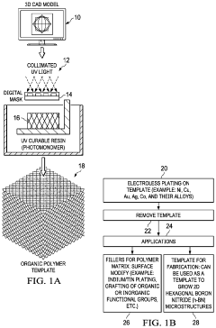
Hexagonal boron nitride structures
PatentPendingUS20220250909A1
Innovation
- A method involving the use of a self-propagating photopolymer waveguide technique to create a 3D metal microlattice template, followed by electroless metal plating and subsequent growth of h-BN on the metal surface, allowing for the formation of regular, ordered h-BN nanostructures with controlled dimensions and properties.
Isotropic boron nitride, method of manufacture thereof and articles made therefrom
PatentWO2018013624A1
Innovation
- The method involves combining anisotropic boron nitride with a supercritical fluid to expand the interstices between crystal layers, disrupting the anisotropic platelet structure and resulting in isotropic boron nitride with uniform thermal and mechanical properties in all dimensions.
Environmental Impact and Sustainability of BN Production
The production of boron nitride (BN) substrates presents significant environmental considerations that must be addressed as the material gains prominence in thermal management applications. Traditional BN synthesis methods, particularly chemical vapor deposition (CVD) and high-temperature high-pressure (HTHP) techniques, consume substantial energy and often utilize hazardous precursors such as boron trichloride and ammonia, which pose environmental risks if not properly managed.
Recent life cycle assessments reveal that BN production generates considerable carbon emissions, primarily from the energy-intensive processes requiring temperatures exceeding 1500°C. A single kilogram of high-quality hexagonal BN may contribute up to 30 kg of CO2 equivalent emissions, highlighting the environmental footprint of these advanced materials despite their beneficial thermal properties.
Water usage represents another critical environmental factor, with wet chemical processes for BN purification consuming 15-20 liters of water per kilogram of product. Effluent from these processes contains boron compounds that, if released untreated, can disrupt aquatic ecosystems and potentially contaminate groundwater resources.
Encouragingly, several sustainable innovations are emerging within the industry. Biomass-derived precursors are being developed as alternatives to petroleum-based starting materials, potentially reducing the carbon footprint by 40-60%. Additionally, closed-loop manufacturing systems that recapture and reuse process chemicals have demonstrated water consumption reductions of up to 75% in pilot implementations.
The mechanical durability of BN substrates contributes positively to sustainability through extended product lifecycles. Studies indicate that properly engineered BN substrates maintain thermal performance for 5-7 years in demanding electronic applications, compared to 2-3 years for conventional materials, thereby reducing replacement frequency and associated environmental impacts.
End-of-life considerations for BN materials present both challenges and opportunities. While not biodegradable, BN is chemically stable and non-toxic, minimizing leaching concerns in disposal scenarios. Emerging recycling technologies can recover up to 80% of boron from spent BN substrates, though these processes remain energy-intensive and not yet widely implemented.
Regulatory frameworks are increasingly influencing BN production sustainability, with the European Union's REACH regulations and similar global initiatives requiring manufacturers to document environmental impacts and implement mitigation strategies. Forward-thinking companies are proactively adopting green chemistry principles and investing in renewable energy sources for production facilities, positioning sustainability as a competitive advantage in the growing thermal management materials market.
Integration Challenges with Electronic Device Manufacturing
The integration of boron nitride (BN) substrates into electronic device manufacturing presents significant challenges despite their promising thermal and mechanical properties. Current semiconductor fabrication processes are highly optimized for silicon and other conventional materials, requiring substantial modifications to accommodate BN substrates. These adaptations often necessitate redesigning entire production lines, which involves considerable capital investment and technical expertise.
Surface compatibility issues represent another major hurdle. BN's hexagonal structure and predominantly covalent bonding characteristics create difficulties in achieving reliable metal contacts and interconnects. The formation of ohmic contacts, essential for efficient device operation, requires specialized deposition techniques and often additional interface layers to overcome the inherent chemical inertness of BN surfaces.
Thermal expansion mismatch between BN substrates and other device components introduces stress during thermal cycling, potentially leading to delamination, cracking, or performance degradation over time. While BN offers excellent thermal conductivity, managing the differential expansion at material interfaces remains problematic, particularly in applications involving extreme temperature variations.
Scalability concerns further complicate integration efforts. Current methods for producing high-quality BN substrates with consistent properties at wafer-scale dimensions lag behind those for conventional semiconductor materials. The synthesis of large-area, defect-free BN films with uniform thickness and crystallinity continues to challenge manufacturers, limiting mass production capabilities and increasing costs.
Etching and patterning processes also require significant adaptation. Traditional photolithography and etching techniques developed for silicon processing show limited effectiveness with BN substrates. The chemical stability that makes BN attractive for harsh environments simultaneously makes precise microfabrication more difficult, necessitating development of specialized etchants and masking materials.
Device encapsulation and packaging present additional integration challenges. The interface between BN substrates and packaging materials must maintain thermal performance while ensuring mechanical integrity. Conventional packaging solutions often fail to capitalize on BN's thermal advantages, creating bottlenecks that limit overall system performance despite the substrate's inherent capabilities.
Addressing these integration challenges requires collaborative efforts between materials scientists, process engineers, and device designers. Innovative approaches such as transfer-free growth methods, interface engineering techniques, and hybrid integration strategies show promise for overcoming these obstacles and enabling broader adoption of BN substrates in next-generation electronic devices.
Unlock deeper insights with Patsnap Eureka Quick Research — get a full tech report to explore trends and direct your research. Try now!
Generate Your Research Report Instantly with AI Agent
Supercharge your innovation with Patsnap Eureka AI Agent Platform!