Boron Nitride For High-Frequency PCBs: Dk/Df Stability, Copper Adhesion And Reliability
SEP 12, 20259 MIN READ
Generate Your Research Report Instantly with AI Agent
Patsnap Eureka helps you evaluate technical feasibility & market potential.
BN for HF PCBs: Background and Objectives
Boron Nitride (BN) has emerged as a promising material for high-frequency printed circuit boards (PCBs) due to its exceptional thermal and electrical properties. The evolution of electronic devices towards higher frequencies, particularly in 5G, radar systems, and satellite communications, has created unprecedented demands on PCB materials. Traditional FR-4 and other conventional substrates face significant limitations at frequencies above 10 GHz, including signal loss, dielectric constant instability, and thermal management challenges.
The historical development of PCB materials shows a clear trajectory from simple phenolic boards to advanced composites. In the 1960s and 1970s, FR-4 became the industry standard, but as operating frequencies increased beyond 1 GHz in the 1990s, its limitations became apparent. This led to the development of specialized high-frequency materials like PTFE-based substrates. The 2000s witnessed the introduction of ceramic-filled hydrocarbon materials, and now, in the 2020s, we are seeing the emergence of advanced materials like BN composites.
Boron Nitride, particularly in its hexagonal form (h-BN), offers a unique combination of properties that address critical challenges in high-frequency applications. With a crystal structure similar to graphite, h-BN provides excellent thermal conductivity (up to 400 W/m·K in-plane), high temperature stability (up to 1000°C in air), and most importantly for PCB applications, a low dielectric constant (Dk ≈ 4) with minimal variation across frequency ranges and temperatures.
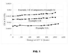
The primary technical objectives for BN integration in high-frequency PCBs include achieving consistent dielectric constant (Dk) and dissipation factor (Df) across broad frequency ranges (DC to 100+ GHz) and temperature variations (-55°C to +125°C). Additionally, ensuring strong copper adhesion to BN-enhanced substrates remains critical for manufacturing reliability and long-term performance under thermal cycling conditions.
Current research focuses on optimizing BN particle size, distribution, and surface functionalization to enhance compatibility with traditional PCB resin systems while maintaining processability. The goal is to develop commercially viable manufacturing processes that can incorporate BN into existing PCB production lines without requiring extensive retooling or process modifications.
The successful development of BN-enhanced high-frequency PCB materials could enable significant advancements in telecommunications infrastructure, aerospace systems, automotive radar, and next-generation computing devices. This technology represents a critical enabler for the continued miniaturization and performance enhancement of electronic systems operating at increasingly higher frequencies.
The historical development of PCB materials shows a clear trajectory from simple phenolic boards to advanced composites. In the 1960s and 1970s, FR-4 became the industry standard, but as operating frequencies increased beyond 1 GHz in the 1990s, its limitations became apparent. This led to the development of specialized high-frequency materials like PTFE-based substrates. The 2000s witnessed the introduction of ceramic-filled hydrocarbon materials, and now, in the 2020s, we are seeing the emergence of advanced materials like BN composites.
Boron Nitride, particularly in its hexagonal form (h-BN), offers a unique combination of properties that address critical challenges in high-frequency applications. With a crystal structure similar to graphite, h-BN provides excellent thermal conductivity (up to 400 W/m·K in-plane), high temperature stability (up to 1000°C in air), and most importantly for PCB applications, a low dielectric constant (Dk ≈ 4) with minimal variation across frequency ranges and temperatures.
The primary technical objectives for BN integration in high-frequency PCBs include achieving consistent dielectric constant (Dk) and dissipation factor (Df) across broad frequency ranges (DC to 100+ GHz) and temperature variations (-55°C to +125°C). Additionally, ensuring strong copper adhesion to BN-enhanced substrates remains critical for manufacturing reliability and long-term performance under thermal cycling conditions.
Current research focuses on optimizing BN particle size, distribution, and surface functionalization to enhance compatibility with traditional PCB resin systems while maintaining processability. The goal is to develop commercially viable manufacturing processes that can incorporate BN into existing PCB production lines without requiring extensive retooling or process modifications.
The successful development of BN-enhanced high-frequency PCB materials could enable significant advancements in telecommunications infrastructure, aerospace systems, automotive radar, and next-generation computing devices. This technology represents a critical enabler for the continued miniaturization and performance enhancement of electronic systems operating at increasingly higher frequencies.
Market Analysis for High-Frequency PCB Materials
The high-frequency PCB materials market is experiencing robust growth driven by the increasing demand for high-speed data transmission and processing capabilities across multiple industries. Currently valued at approximately $2.3 billion, this specialized segment is projected to grow at a CAGR of 7.8% through 2028, significantly outpacing the broader PCB materials market.
The telecommunications sector remains the largest consumer of high-frequency PCB materials, accounting for nearly 40% of market demand. This is primarily fueled by the ongoing global 5G infrastructure deployment and preparation for future 6G technologies. The automotive industry represents the fastest-growing segment with 12.3% annual growth, driven by the rapid adoption of advanced driver assistance systems (ADAS), autonomous driving technologies, and vehicle-to-everything (V2X) communication systems.
Regionally, Asia-Pacific dominates the market with 58% share, led by manufacturing powerhouses in China, Taiwan, and South Korea. North America follows with 22% market share, where demand is primarily driven by aerospace, defense, and cutting-edge telecommunications applications. Europe accounts for 17% of the market, with particular strength in automotive and industrial applications.
From a materials perspective, PTFE-based laminates currently dominate with approximately 45% market share due to their established performance characteristics. However, newer materials including modified epoxy, hydrocarbon ceramics, and particularly boron nitride composites are gaining significant traction. Boron nitride-based materials specifically are projected to achieve the highest growth rate at 14.2% annually through 2028.
Key market drivers include the exponential increase in data traffic, proliferation of IoT devices, miniaturization of electronic components, and the push toward higher operating frequencies. The demand for materials with superior Dk/Df stability across wide frequency ranges (up to 110 GHz) has become particularly critical as applications move into millimeter-wave territory.
Price sensitivity varies significantly by application segment. While consumer electronics manufacturers remain highly cost-conscious, aerospace and defense applications prioritize performance and reliability over cost considerations. This bifurcation creates distinct market dynamics where material innovations must balance performance improvements against cost implications depending on the target application segment.
The competitive landscape features established players like Rogers Corporation, Isola Group, and Panasonic, alongside emerging specialists focused on next-generation materials. Recent market consolidation through mergers and acquisitions indicates the strategic importance of high-performance materials portfolios for maintaining competitive advantage in this rapidly evolving sector.
Current Challenges in BN-Based PCB Technology
Despite the promising properties of boron nitride (BN) for high-frequency PCB applications, several significant technical challenges currently impede its widespread industrial adoption. The primary obstacle lies in achieving consistent dielectric constant (Dk) and dissipation factor (Df) stability across varying frequencies and temperatures. While BN demonstrates excellent theoretical performance, maintaining these properties in actual manufacturing environments has proven difficult, particularly when BN is incorporated into composite materials with epoxy resins.
Copper adhesion represents another critical challenge for BN-enhanced PCB substrates. The inherently smooth and chemically inert surface of BN particles creates weak interfacial bonding with copper foil, resulting in delamination issues during thermal cycling and mechanical stress. Current surface treatment methods often compromise the thermal conductivity advantages that make BN attractive in the first place.
Moisture absorption poses a significant reliability concern, as BN-filled composites can exhibit hygroscopic tendencies depending on the matrix material and processing conditions. This moisture uptake directly impacts electrical performance stability and can accelerate aging mechanisms in high-frequency applications, particularly in humid environments.
Manufacturing scalability remains problematic, with difficulties in achieving homogeneous BN dispersion throughout the resin matrix. Agglomeration of BN particles creates localized variations in dielectric properties and thermal conductivity, leading to inconsistent performance across the PCB substrate. Current mixing and dispersion technologies struggle to maintain uniformity at higher BN loading percentages (>30% by weight) needed for optimal thermal performance.
Cost factors present substantial barriers to commercialization, as high-purity hexagonal BN remains significantly more expensive than traditional fillers. The additional processing steps required for surface modification and proper dispersion further increase manufacturing costs, making BN-enhanced PCBs economically viable only for specialized high-performance applications.
Thermal expansion mismatch between BN particles and surrounding matrix materials creates internal stresses during temperature cycling, potentially leading to microcrack formation and reliability issues in multilayer structures. This becomes particularly problematic in applications requiring frequent thermal cycling or operation across wide temperature ranges.
Environmental and regulatory considerations also pose challenges, as the long-term environmental impact and end-of-life recycling options for BN-enhanced composites remain inadequately studied, potentially limiting adoption in industries with strict sustainability requirements.
Current BN Integration Methods for PCBs
01 Boron Nitride for Dielectric Constant/Dissipation Factor Stability
Boron nitride is utilized in electronic materials to provide stable dielectric properties (Dk/Df) across varying frequencies and temperatures. The hexagonal crystal structure of boron nitride contributes to its excellent thermal stability and low dielectric loss, making it ideal for high-frequency applications. Formulations containing boron nitride can maintain consistent electrical performance even under harsh environmental conditions, which is crucial for reliable electronic components.- Boron Nitride for Dielectric Constant (Dk) and Dissipation Factor (Df) Stability: Boron nitride is incorporated into composite materials to enhance dielectric constant (Dk) and dissipation factor (Df) stability across various frequencies and temperatures. The hexagonal crystal structure of boron nitride contributes to low dielectric loss and consistent electrical performance, making it suitable for high-frequency electronic applications. These properties remain stable even under harsh environmental conditions, providing reliable performance in advanced electronic systems.
- Copper Adhesion Enhancement with Boron Nitride Composites: Boron nitride-based composites can be formulated to improve copper adhesion in electronic substrates and circuit boards. Surface treatments and coupling agents are used to modify boron nitride particles, enhancing their compatibility with resin systems and promoting stronger interfacial bonding with copper layers. These formulations address the inherent challenge of poor adhesion between boron nitride's inert surface and metal layers, resulting in more reliable electronic interconnects with improved peel strength and mechanical durability.
- Thermal Management and Reliability Improvements: Boron nitride's excellent thermal conductivity properties are utilized to enhance the reliability of electronic components by efficiently dissipating heat. When incorporated into substrate materials, boron nitride creates thermally conductive pathways that reduce hotspots and thermal stress in high-power electronic applications. This thermal management capability helps maintain stable electrical properties and extends the operational lifetime of electronic devices, particularly in demanding environments with thermal cycling.
- Moisture Resistance and Environmental Stability: Boron nitride composites can be engineered to provide superior moisture resistance and environmental stability for electronic applications. By incorporating hydrophobic additives or surface treatments, these materials maintain their electrical and mechanical properties even under high humidity conditions. This moisture resistance prevents degradation of dielectric properties and copper adhesion over time, ensuring long-term reliability in various operating environments and reducing failure rates in electronic assemblies.
- Processing Techniques for Optimized Boron Nitride Performance: Specialized processing techniques are employed to optimize boron nitride's performance in electronic substrate applications. These include controlled particle size distribution, orientation of hexagonal boron nitride platelets, and advanced dispersion methods to achieve uniform distribution within the matrix material. Such processing approaches maximize the beneficial properties of boron nitride while minimizing potential negative impacts on manufacturability, resulting in materials with balanced electrical, thermal, and mechanical characteristics suitable for high-reliability electronic applications.
02 Copper Adhesion Enhancement with Boron Nitride Composites
Boron nitride can be incorporated into composite materials to improve copper adhesion in electronic substrates. Surface treatments and functionalization of boron nitride particles create stronger interfacial bonding with copper layers. These composites often include coupling agents or adhesion promoters that enhance the interaction between the boron nitride filler and copper surfaces, resulting in improved peel strength and mechanical integrity of copper-clad laminates used in circuit boards.Expand Specific Solutions03 Thermal Management and Reliability Improvement
Boron nitride's excellent thermal conductivity helps dissipate heat in electronic components, thereby enhancing reliability. When incorporated into substrate materials, it reduces thermal stress between copper traces and the underlying dielectric, preventing delamination and improving long-term reliability. The thermal stability of boron nitride also contributes to maintaining consistent electrical performance across temperature fluctuations, which is essential for applications requiring high reliability under thermal cycling conditions.Expand Specific Solutions04 Boron Nitride Particle Size and Distribution Effects
The size, shape, and distribution of boron nitride particles significantly impact the dielectric properties and copper adhesion in electronic materials. Nano-sized boron nitride particles can provide improved dispersion and interfacial contact with the polymer matrix, leading to enhanced dielectric stability. Controlled particle size distribution helps optimize the balance between dielectric performance and mechanical properties, while also influencing the surface roughness that affects copper adhesion strength.Expand Specific Solutions05 Environmental Resistance and Long-term Reliability
Boron nitride enhances the moisture resistance and chemical stability of electronic materials, contributing to long-term reliability. Composites containing boron nitride show improved resistance to moisture absorption, which helps maintain stable dielectric properties in humid environments. The chemical inertness of boron nitride also protects against oxidation and degradation of the interface between copper and dielectric materials, extending the service life of electronic components under various environmental stresses.Expand Specific Solutions
Leading Manufacturers and Research Institutions
The boron nitride high-frequency PCB market is currently in a growth phase, with increasing demand driven by 5G, aerospace, and defense applications requiring superior thermal and electrical performance. The market is projected to expand significantly as high-frequency communication technologies proliferate. Technologically, boron nitride PCB materials are advancing toward commercial maturity, with key players demonstrating varied capabilities. Mitsubishi Materials, Sumitomo Electric, and Shengyi Technology lead in commercial applications, while Denka and Resonac Holdings focus on material innovations. Academic institutions like Rice University and Harbin Institute of Technology contribute fundamental research, particularly in copper adhesion and reliability challenges. The competitive landscape features both established materials conglomerates and specialized manufacturers working to address Dk/Df stability requirements for next-generation electronics.
Sumitomo Electric Industries Ltd.
Technical Solution: Sumitomo Electric has developed a sophisticated BN-based high-frequency PCB material system utilizing their proprietary "controlled orientation" technology. Their approach aligns hexagonal boron nitride platelets (2-8μm diameter) in the horizontal plane during the manufacturing process, creating anisotropic electrical properties that minimize signal loss in the z-direction while maintaining excellent in-plane performance. The materials demonstrate Dk values of 3.2-3.6 with Df below 0.002 at frequencies up to 80 GHz, with less than 2% variation across temperature ranges from -65°C to +150°C. Sumitomo's copper adhesion technology incorporates a multi-layer approach with a specialized transition layer between the copper foil and the BN-composite substrate. This transition layer contains graduated concentrations of coupling agents and nano-adhesion promoters, achieving peel strengths of 1.3-1.5 kN/m that remain stable even after 1000 hours of high-temperature, high-humidity exposure (85°C/85% RH).
Strengths: Exceptional signal integrity through controlled BN orientation; superior environmental reliability; excellent thermal stability across extreme temperature ranges. Weaknesses: Complex manufacturing process requiring precise control of material flow and curing conditions; higher cost structure; longer lead times for specialized formulations.
Denka Corp.
Technical Solution: Denka Corporation has developed a comprehensive BN-based solution for high-frequency PCB applications through their "HFSS" (High-Frequency Stable Substrate) technology platform. Their approach utilizes spherical boron nitride particles (1-3μm diameter) with specialized surface treatments to enhance compatibility with various resin systems. The materials exhibit Dk values of 3.0-3.8 with Df values of 0.002-0.004 across frequencies from 1-60 GHz, maintaining stability within ±2% across this range. Denka's copper adhesion technology employs a dual-mechanism approach combining mechanical anchoring through controlled copper surface roughness (Rz 4-8μm) and chemical bonding through specialized silane coupling agents that form covalent bonds between the copper oxide layer and the BN-resin matrix. Their materials demonstrate excellent reliability with CAF resistance exceeding 1000 hours under bias-humidity-temperature conditions (85°C/85%RH/50V) and thermal reliability through 500+ thermal shock cycles (-65°C to +150°C).
Strengths: Well-balanced electrical and mechanical properties; excellent CAF resistance for long-term reliability; compatible with standard PCB manufacturing processes. Weaknesses: Moderate thermal conductivity compared to some competitors; slightly higher insertion loss at frequencies above 40 GHz; requires careful process control during lamination.
Key Patents and Research on BN Dielectric Properties
High dielectric strength insulator
PatentInactiveUS20210134478A1
Innovation
- A composite insulator solution using boron nitride as a base material coated with a high-purity SiO2 or diamond layer, ensuring high ac dielectric strength, mechanical robustness, and resistance to water absorption and abrasion, achieved through specific machining and coating processes.
h-BORON NITRIDE AND POLYCYCLIC-OLEFINIC POLYMER CONTAINING OLEFINIC FUNCTIONALITY FOR FORMING LOW-LOSS FILMS HAVING IMPROVED DIELECTRIC AND THERMAL PROPERTIES
PatentPendingUS20240110038A1
Innovation
- A composition comprising polymers formed from polycyclic olefinic monomers, hexagonal boron nitride, a crosslinker, a tackifier, and a free radical initiator, which allows for the creation of films with unprecedented dielectric and thermal properties, including low dielectric constant, low loss, and high glass transition temperature.
Thermal Management Capabilities of BN in PCBs
Boron Nitride (BN) has emerged as a critical material for thermal management in high-frequency PCBs due to its exceptional thermal conductivity properties. With thermal conductivity values ranging from 30 to 300 W/mK depending on crystalline structure and purity, BN significantly outperforms traditional PCB materials like FR-4 (typically 0.3 W/mK) and even rivals some metallic heat spreaders in specific applications.
The hexagonal form of BN (h-BN) demonstrates particularly impressive thermal management capabilities when incorporated into PCB substrates. Research indicates that even modest additions of 10-15% BN can increase thermal conductivity by 5-10 times compared to standard epoxy composites. This enhancement enables more efficient heat dissipation from high-power components, reducing thermal resistance and hotspot formation that typically limit the performance of high-frequency circuits.
BN's thermal management advantages extend beyond simple conductivity metrics. The material exhibits thermal stability across a wide temperature range (-270°C to 900°C in non-oxidizing environments), maintaining consistent performance even during thermal cycling. This stability is crucial for high-reliability applications where thermal expansion mismatch can lead to mechanical stress and eventual failure.
Recent studies have demonstrated that BN-enhanced PCB materials show reduced z-axis thermal resistance, addressing a common bottleneck in multilayer board designs. The anisotropic thermal properties of h-BN can be leveraged through alignment techniques during manufacturing to create preferential heat flow paths, directing thermal energy away from sensitive components or toward designated heat dissipation structures.
Another significant advantage is BN's electrical insulation properties, which allow it to improve thermal performance without compromising the electrical isolation requirements of high-frequency circuits. This dual functionality eliminates the need for separate thermal management solutions that might otherwise introduce additional interfaces and thermal resistances.
Field testing of BN-enhanced PCBs in high-power RF applications has shown operating temperature reductions of 15-30°C compared to conventional materials under identical power loads. This temperature reduction directly translates to improved reliability, with industry models suggesting a potential doubling of mean time between failures (MTBF) for every 10°C reduction in operating temperature.
The implementation of BN in PCB thermal management systems also enables more compact designs by reducing or eliminating the need for additional heat sinks or cooling systems, contributing to overall miniaturization trends in electronic devices while maintaining or improving thermal performance parameters.
Environmental Impact and Sustainability Considerations
The environmental impact of boron nitride (BN) in high-frequency PCB applications represents a critical consideration as electronics manufacturers increasingly prioritize sustainability. BN offers several environmental advantages compared to traditional materials, including lower energy consumption during processing due to its thermal stability properties. The reduced need for cooling systems and temperature management in manufacturing processes translates to decreased carbon footprint across the production lifecycle.
BN-enhanced PCBs demonstrate extended operational lifespans due to superior thermal management and electrical stability, directly addressing the growing electronic waste crisis. This longevity reduces replacement frequency and associated resource consumption, aligning with circular economy principles increasingly demanded by regulatory frameworks and consumers alike.
The extraction and processing of boron nitride presents mixed environmental implications. While BN requires less energy-intensive processing than some competing materials, mining operations for boron compounds can impact local ecosystems through land disturbance and water usage. Industry leaders are developing more sustainable extraction methods, including closed-loop water systems and rehabilitation protocols for mining sites.
End-of-life considerations for BN-enhanced PCBs present both challenges and opportunities. The strong bonding between BN and copper substrates, while beneficial for performance, may complicate recycling processes. However, emerging separation technologies utilizing selective chemical treatments show promise for efficient material recovery without hazardous byproducts.
Carbon footprint analyses comparing BN-enhanced PCBs to conventional alternatives demonstrate net environmental benefits when considering full lifecycle assessments. The reduced energy consumption during operation, extended product lifespan, and potential for material recovery collectively offset the initial production impacts.
Regulatory compliance represents another dimension of BN sustainability. The material's inert nature aligns well with RoHS and REACH regulations, avoiding restricted substances common in alternative solutions. This compliance simplifies global market access while reducing potential environmental hazards throughout the product lifecycle.
Industry adoption of BN technology must be accompanied by responsible sourcing initiatives and transparent supply chain documentation. Leading manufacturers are establishing certification programs verifying ethical mining practices and environmental stewardship throughout the BN supply chain, addressing growing stakeholder concerns regarding material provenance and ecological impact.
Unlock deeper insights with Patsnap Eureka Quick Research — get a full tech report to explore trends and direct your research. Try now!
Generate Your Research Report Instantly with AI Agent
Supercharge your innovation with Patsnap Eureka AI Agent Platform!