How Can Semiconductor Innovations Improve Wearable Biosensors
OCT 24, 202510 MIN READ
Generate Your Research Report Instantly with AI Agent
Patsnap Eureka helps you evaluate technical feasibility & market potential.
Semiconductor Biosensor Evolution and Objectives
Semiconductor technology has undergone remarkable evolution since the invention of the first transistor in 1947. This progression has been characterized by continuous miniaturization, increased computational power, and reduced energy consumption, following Moore's Law for decades. In the context of biosensors, semiconductor technology has transformed from simple silicon-based sensors to complex integrated systems capable of real-time physiological monitoring. The integration of semiconductor technology with biosensing capabilities began in the 1980s with the development of ion-sensitive field-effect transistors (ISFETs), which marked the first significant application of semiconductor principles to biological sensing.
The 2000s witnessed accelerated development with the emergence of lab-on-chip technologies and microelectromechanical systems (MEMS), enabling more sophisticated biosensing capabilities. Recent advancements have focused on flexible electronics, nanomaterials integration, and ultra-low power consumption designs, which are particularly crucial for wearable applications. The convergence of semiconductor technology with wireless communication, artificial intelligence, and energy harvesting has further expanded the capabilities of wearable biosensors.
Current technological objectives in semiconductor-based wearable biosensors center around several key areas. First is the enhancement of sensor sensitivity and specificity to detect biomarkers at increasingly lower concentrations, approaching single-molecule detection in some cases. This is essential for early disease detection and precise health monitoring. Second is the development of multimodal sensing platforms capable of simultaneously monitoring various physiological parameters, providing a more comprehensive health assessment.
Power efficiency represents another critical objective, with research focused on reducing energy consumption to extend device operation time between charges or enable self-powered operation through energy harvesting. Miniaturization continues to be a priority, with efforts directed toward developing smaller, lighter, and more comfortable wearable devices without compromising functionality. Biocompatibility and durability are equally important, as these devices must maintain performance while in prolonged contact with biological tissues.
The integration of advanced data processing capabilities directly within the sensor platform constitutes a significant objective, enabling edge computing for real-time analysis and reducing dependency on external devices. Additionally, there is a growing emphasis on developing standardized fabrication processes that can facilitate mass production while maintaining quality and reducing costs, thereby accelerating market adoption of these technologies.
These technological objectives collectively aim to transform wearable biosensors from specialized medical devices to ubiquitous health monitoring tools, capable of continuous, non-invasive, and comprehensive health assessment in everyday settings.
Market Analysis for Advanced Wearable Health Monitoring
The wearable health monitoring market is experiencing unprecedented growth, driven by increasing health consciousness, aging populations, and technological advancements. The global market for advanced wearable health monitoring devices was valued at approximately $13.8 billion in 2022 and is projected to reach $37.4 billion by 2028, representing a compound annual growth rate (CAGR) of 18.3%. This remarkable expansion reflects the growing consumer demand for continuous health tracking and preventive healthcare solutions.
Consumer preferences are shifting toward non-invasive, comfortable, and accurate monitoring devices that seamlessly integrate into daily life. The COVID-19 pandemic has accelerated this trend, with heightened awareness of personal health metrics creating a surge in demand for devices capable of monitoring vital signs such as heart rate, blood oxygen levels, and respiratory patterns. Market research indicates that over 60% of consumers now consider health monitoring features essential when purchasing wearable technology.
Healthcare providers and insurance companies have become significant market drivers, increasingly incorporating wearable health data into patient care protocols and insurance models. This institutional adoption has created a robust B2B segment alongside the traditional consumer market. Hospitals and clinics are implementing remote patient monitoring systems that rely on advanced wearable sensors, creating a market segment expected to grow at 22.1% CAGR through 2028.
Regional analysis reveals North America currently dominates the market with approximately 42% share, followed by Europe (28%) and Asia-Pacific (23%). However, the Asia-Pacific region is expected to witness the fastest growth rate due to increasing healthcare expenditure, rising disposable incomes, and growing digital health initiatives in countries like China, Japan, and India.
Key market segments include smartwatches (38% market share), fitness bands (27%), smart clothing (12%), and medical-grade wearables (23%). The medical-grade segment, which includes continuous glucose monitors, ECG monitors, and blood pressure monitors, is projected to grow most rapidly at 24.5% CAGR, driven by increasing regulatory approvals and integration with telehealth platforms.
Consumer adoption barriers include concerns about data privacy (cited by 58% of non-users), accuracy limitations (47%), and device comfort (39%). These challenges present significant opportunities for semiconductor innovations that can address size constraints, power consumption, and sensor accuracy while maintaining data security and user comfort.
The competitive landscape features established technology companies (Apple, Samsung, Fitbit/Google), medical device manufacturers (Medtronic, Abbott), and specialized wearable health startups. Recent market trends indicate increasing partnerships between semiconductor manufacturers and wearable device companies to develop custom chips optimized for health monitoring applications.
Current Semiconductor Technologies and Limitations in Biosensing
The semiconductor industry has been pivotal in advancing wearable biosensor technologies through continuous miniaturization and integration capabilities. Current semiconductor technologies employed in biosensing applications primarily include complementary metal-oxide-semiconductor (CMOS) platforms, which serve as the foundation for most modern biosensors due to their low power consumption and high integration density. These platforms enable the development of system-on-chip (SoC) solutions that incorporate sensing, signal processing, and wireless communication functionalities within a single compact device.
Flexible and stretchable electronics represent another significant advancement, utilizing thin-film transistors (TFTs) and organic semiconductors to create conformable sensors that adapt to body contours. These technologies have enabled the development of skin-like electronic patches and textile-integrated sensors that offer improved comfort and continuous monitoring capabilities without restricting user mobility.
Microelectromechanical systems (MEMS) technology has facilitated the creation of miniaturized mechanical structures integrated with semiconductor devices, allowing for highly sensitive physical measurements such as acceleration, pressure, and temperature. In biosensing applications, MEMS-based sensors can detect minute biological signals with remarkable precision while maintaining small form factors suitable for wearable devices.
Despite these advancements, current semiconductor technologies face several limitations in biosensing applications. Power consumption remains a significant challenge, as continuous monitoring requires substantial energy that current battery technologies struggle to provide efficiently. This constraint often forces compromises between functionality, monitoring duration, and device size, limiting the practical utility of many wearable biosensors.
Signal-to-noise ratio (SNR) presents another critical limitation, particularly when measuring subtle biological signals in noisy environments. Interference from motion artifacts, electromagnetic radiation, and other environmental factors can significantly degrade measurement accuracy, necessitating sophisticated signal processing algorithms that further increase power demands.
Biocompatibility issues also persist with many semiconductor materials, potentially causing skin irritation or allergic reactions during prolonged contact. Additionally, the hermeticity of packaging remains challenging, as bodily fluids and sweat can compromise electronic components over time, reducing device longevity and reliability.
Manufacturing scalability presents another barrier, with advanced semiconductor processes often requiring specialized facilities and significant capital investment. This challenge is particularly pronounced for novel materials and flexible substrates, which may not be compatible with standard semiconductor fabrication processes, thereby increasing production costs and limiting widespread adoption.
Interoperability between different sensing modalities and communication protocols further complicates the development of comprehensive biosensing solutions, often resulting in fragmented ecosystems that hinder data integration and analysis across platforms.
Existing Semiconductor Solutions for Wearable Biosensors
01 Advanced semiconductor manufacturing processes
Innovations in semiconductor manufacturing processes have led to significant advancements in the industry. These include improved fabrication techniques, enhanced lithography methods, and novel material integration approaches that enable the production of smaller, more efficient semiconductor devices. These manufacturing innovations help overcome physical limitations and continue the scaling trends predicted by Moore's Law, allowing for higher transistor densities and improved performance.- Advanced semiconductor manufacturing processes: Innovations in semiconductor manufacturing processes have led to significant improvements in chip performance and efficiency. These advancements include new lithography techniques, novel materials integration, and enhanced fabrication methods that enable smaller feature sizes and higher transistor densities. Such manufacturing innovations are crucial for continuing Moore's Law and meeting the demands of modern computing applications.
- Semiconductor device architecture innovations: Novel semiconductor device architectures have been developed to overcome traditional scaling limitations. These innovations include three-dimensional transistor designs, gate-all-around structures, and advanced packaging technologies that improve performance while reducing power consumption. Such architectural innovations enable continued advancement in semiconductor capabilities even as conventional scaling approaches physical limits.
- AI and machine learning integration in semiconductor technology: Artificial intelligence and machine learning are being increasingly integrated into semiconductor design and manufacturing processes. These technologies enable more efficient chip design, defect detection, yield optimization, and performance prediction. The combination of AI with semiconductor technology is creating smarter chips that can better handle complex computational tasks while improving overall production efficiency.
- Energy-efficient semiconductor solutions: Energy efficiency has become a critical focus in semiconductor innovation, leading to the development of low-power designs and technologies. These innovations include advanced power management circuits, reduced leakage current techniques, and energy-harvesting capabilities. Such developments are essential for extending battery life in mobile devices and reducing the environmental impact of computing infrastructure.
- Specialized semiconductor technologies for emerging applications: Specialized semiconductor technologies are being developed for emerging applications such as quantum computing, neuromorphic computing, and advanced sensors. These innovations include novel materials, unique circuit designs, and specialized fabrication techniques tailored to specific application requirements. Such specialized semiconductor technologies are enabling new capabilities in fields ranging from autonomous vehicles to advanced medical devices.
02 Semiconductor materials and device structures
Novel semiconductor materials and device structures represent a significant area of innovation. This includes the development of compound semiconductors, two-dimensional materials, and advanced transistor architectures such as FinFETs, gate-all-around structures, and vertical designs. These innovations enable improved electrical characteristics, reduced power consumption, and enhanced performance for various applications including computing, communications, and power electronics.Expand Specific Solutions03 AI and machine learning in semiconductor design
Artificial intelligence and machine learning technologies are revolutionizing semiconductor design and optimization. These computational approaches enable more efficient exploration of design spaces, prediction of device performance, automation of complex design tasks, and optimization of manufacturing processes. By leveraging AI, semiconductor companies can reduce development time, improve yields, and create more innovative chip designs that meet increasingly complex requirements.Expand Specific Solutions04 Power and energy efficiency innovations
Energy efficiency has become a critical focus in semiconductor innovation, addressing the growing power consumption challenges in electronic devices. Innovations include low-power circuit designs, dynamic power management techniques, and novel materials that reduce leakage current. These advancements enable semiconductor devices to operate with significantly lower power requirements while maintaining or improving performance, which is particularly important for mobile devices, IoT applications, and data centers.Expand Specific Solutions05 Specialized semiconductor technologies for emerging applications
Semiconductor innovations are increasingly focused on specialized technologies for emerging applications such as quantum computing, neuromorphic computing, and advanced sensing. These include the development of specialized integrated circuits, novel memory technologies, and sensor integration approaches. Such innovations enable new capabilities in fields ranging from autonomous vehicles and advanced robotics to next-generation computing paradigms and biomedical applications.Expand Specific Solutions
Leading Companies in Semiconductor Biosensor Development
The wearable biosensor market is experiencing rapid growth, driven by semiconductor innovations that enhance functionality, accuracy, and miniaturization. Currently in its growth phase, the market is projected to expand significantly as healthcare monitoring shifts toward continuous, personalized solutions. Key players like Taiwan Semiconductor Manufacturing Co. and Samsung Electronics are advancing chip miniaturization and power efficiency, while specialized companies such as Infineon Technologies and Renesas Electronics focus on sensor integration and low-power solutions. Academic institutions including California Institute of Technology and University of Southern California collaborate with industry leaders like IBM and Philips to develop next-generation biosensing technologies, creating a competitive landscape where semiconductor innovations are critical for market differentiation and addressing challenges in power consumption, sensitivity, and biocompatibility.
Taiwan Semiconductor Manufacturing Co., Ltd.
Technical Solution: TSMC has developed advanced semiconductor manufacturing processes specifically optimized for wearable biosensors, including their 16nm FinFET Compact Technology (16FFC) and 12nm FFC nodes that balance power efficiency with performance. Their N7 and N5 processes incorporate ultra-low power design techniques that enable biosensors to operate for extended periods on small batteries. TSMC's 3D IC and System-in-Package (SiP) technologies allow for the integration of sensing elements, processing units, and wireless communication modules in compact form factors essential for wearable devices. Their specialized BioSiP platform integrates analog front-end circuits with digital signal processing capabilities in a single package, reducing the overall footprint while improving signal integrity for sensitive biosensor applications[1]. TSMC has also developed specialized analog and mixed-signal process variants that offer enhanced sensitivity for detecting minute biological signals.
Strengths: Industry-leading manufacturing capabilities with the most advanced process nodes; extensive experience in low-power semiconductor design; comprehensive IP ecosystem supporting biosensor applications. Weaknesses: As a pure-play foundry, TSMC depends on partners for complete biosensor system design; limited direct consumer-facing experience may impact understanding of end-user requirements.
Samsung Electronics Co., Ltd.
Technical Solution: Samsung has pioneered the Bio-Processor platform specifically designed for wearable health monitoring devices. This all-in-one solution integrates multiple processing cores, DSP, memory, and power management in a single chip that's 50% smaller than discrete component solutions. Their advanced semiconductor technology incorporates AFE (Analog Front End) circuits capable of processing five different biometric signals simultaneously: bioelectrical impedance analysis, photoplethysmogram, electrocardiogram, skin temperature, and galvanic skin response[2]. Samsung's 5nm EUV process technology enables ultra-low power consumption crucial for continuous monitoring in wearable devices. Their BioActive Sensor combines three health sensors (optical heart rate, electrical heart signal, and bioelectrical impedance analysis) into one compact unit, reducing component count and power requirements by approximately 30%. Samsung has also developed flexible semiconductor substrates that can conform to body contours, improving sensor contact and data reliability while enhancing user comfort[3].
Strengths: Vertical integration from semiconductor manufacturing to end-user devices provides complete ecosystem control; extensive consumer electronics experience informs practical design considerations; strong R&D capabilities across multiple technology domains. Weaknesses: Proprietary nature of their biosensor platforms may limit third-party innovation and adoption; consumer electronics focus sometimes prioritizes marketable features over clinical validity.
Critical Semiconductor Innovations for Biosensing Applications
Biosensor Device and Related Method
PatentActiveUS20170315084A1
Innovation
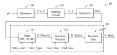
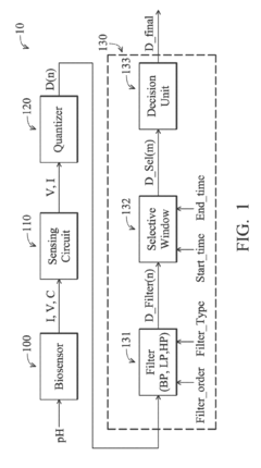
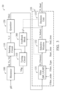
- A biosensor system incorporating a digital filter and selective window to enhance signal-to-noise ratio (SNR) is introduced, along with a feedback network and tuning circuit for self-calibration, allowing for improved signal processing and calibration of biosensors.
Wearable biosensors and applications thereof
PatentActiveUS11813057B2
Innovation
- Development of highly sensitive In2O3 nanoribbon transistor biosensors with integrated on-chip gold gate electrodes, deposited on flexible polyethylene terephthalate substrates, functionalized with glucose oxidase, chitosan, and single-walled carbon nanotubes, capable of detecting glucose concentrations between 10 nM to 1 mM in external body fluids without breaking the skin.
Power Efficiency and Miniaturization Strategies
Power efficiency and miniaturization represent critical challenges in advancing wearable biosensor technology. Semiconductor innovations are driving significant improvements in both areas through several key strategies. The development of ultra-low-power microcontrollers specifically designed for wearable applications has enabled dramatic reductions in energy consumption while maintaining necessary computational capabilities. These specialized processors incorporate advanced power management features such as dynamic voltage scaling and selective power gating that can reduce active power consumption by up to 70% compared to previous generations.
Integration of heterogeneous components through advanced packaging technologies has emerged as another crucial strategy. System-in-Package (SiP) and System-on-Chip (SoC) approaches allow for the combination of sensing elements, processing units, and communication modules within extremely compact form factors. Recent developments in 2.5D and 3D integration techniques have achieved up to 60% reduction in overall device footprint while simultaneously improving signal integrity between components.
Novel semiconductor materials are revolutionizing power efficiency paradigms. Wide-bandgap semiconductors such as gallium nitride (GaN) and silicon carbide (SiC) demonstrate superior performance in power conversion efficiency, enabling smaller power management circuits with reduced thermal dissipation requirements. Additionally, emerging organic and flexible semiconductor technologies facilitate conformable sensor designs that can better adapt to body contours while requiring less structural support material.
Energy harvesting integration represents another frontier in wearable biosensor development. Semiconductor innovations in piezoelectric, thermoelectric, and photovoltaic materials have improved conversion efficiencies, allowing biosensors to supplement battery power with ambient energy sources. These technologies can extend operational lifetimes by 30-200% depending on usage patterns and environmental conditions, reducing battery size requirements.
Advances in analog front-end (AFE) design have significantly improved signal acquisition efficiency. Modern AFEs incorporate adaptive sampling rates, precision analog-to-digital converters, and intelligent noise filtering algorithms implemented directly in silicon. These innovations reduce power consumption while enhancing signal quality, allowing for smaller amplification stages and reduced battery requirements.
The miniaturization of wireless communication components through semiconductor process scaling has enabled dramatic reductions in transceiver size and power requirements. The latest Bluetooth Low Energy (BLE) and ultra-wideband (UWB) chipsets consume up to 80% less power than previous generations while offering improved data rates and reliability, facilitating smaller overall device designs with enhanced functionality.
Biocompatibility and Materials Science Advancements
The advancement of biocompatible materials represents a critical frontier in enhancing wearable biosensor performance and user acceptance. Traditional semiconductor materials often trigger inflammatory responses when in prolonged contact with human tissue, limiting the effectiveness of continuous monitoring devices. Recent innovations in biocompatible polymers, such as polydimethylsiloxane (PDMS) and polyurethane derivatives, have demonstrated significant improvements in reducing adverse biological reactions while maintaining electrical conductivity essential for sensor function.
Semiconductor manufacturers are increasingly exploring hybrid material systems that combine traditional silicon-based components with biocompatible coatings. These developments include ultra-thin graphene layers and biodegradable semiconductor substrates that can safely dissolve after their functional period. The integration of these materials has enabled the creation of "skin-like" electronic systems with mechanical properties closely matching human tissue, dramatically improving comfort during extended wear periods.
Materials science breakthroughs have also addressed the challenge of maintaining sensor accuracy in the presence of bodily fluids. Novel hydrophobic coatings with nanoscale surface modifications can repel moisture while allowing selective permeability to target analytes. This selective permeability represents a significant advancement over previous generations of sensors that often suffered from signal degradation due to biofouling—the accumulation of proteins and other biological materials on sensor surfaces.
The miniaturization of semiconductor components has enabled the development of flexible, stretchable electronic systems that conform to the body's contours. These systems incorporate materials such as liquid metal alloys encased in elastomeric substrates, creating conductive pathways that maintain functionality even when stretched or compressed. This flexibility addresses a key limitation of traditional rigid sensors, which can cause discomfort and produce motion artifacts that compromise data quality.
Emerging research in biomimetic materials—those that imitate biological structures—shows promise for further enhancing biocompatibility. For instance, semiconductor surfaces patterned with microstructures resembling natural tissue topography have demonstrated reduced foreign body responses in preliminary studies. Additionally, the incorporation of anti-inflammatory compounds directly into sensor materials represents a novel approach to mitigating long-term tissue reactions.
The convergence of semiconductor technology with advanced biomaterials science has also enabled progress in self-healing materials that can repair minor damage, extending device lifespan and reliability. These materials incorporate microcapsules containing conductive fluids that release upon mechanical damage, restoring electrical pathways and maintaining sensor functionality even after physical stress or wear.
Unlock deeper insights with Patsnap Eureka Quick Research — get a full tech report to explore trends and direct your research. Try now!
Generate Your Research Report Instantly with AI Agent
Supercharge your innovation with Patsnap Eureka AI Agent Platform!