How Chiplets Aid in the Advancement of Integrated Circuit Design?
JUL 16, 20259 MIN READ
Generate Your Research Report Instantly with AI Agent
Patsnap Eureka helps you evaluate technical feasibility & market potential.
Chiplet Technology Evolution and Objectives
Chiplet technology has emerged as a revolutionary approach in integrated circuit design, marking a significant shift from traditional monolithic chip architectures. The evolution of chiplets can be traced back to the early 2010s when semiconductor manufacturers began exploring ways to overcome the limitations of Moore's Law. As transistor scaling became increasingly challenging and costly, the industry sought alternative methods to improve performance and functionality while maintaining cost-effectiveness.
The primary objective of chiplet technology is to disaggregate complex system-on-chip (SoC) designs into smaller, more manageable components. These individual chiplets can be manufactured using different process nodes, optimized for specific functions, and then integrated onto a single package. This approach allows for greater flexibility in design, improved yield, and the ability to mix and match components from various suppliers.
Throughout its evolution, chiplet technology has seen several key milestones. In 2015, AMD introduced its Infinity Fabric interconnect, laying the groundwork for its future chiplet-based processors. Intel followed suit with its EMIB (Embedded Multi-die Interconnect Bridge) technology in 2017, enabling high-bandwidth connections between chiplets. TSMC's introduction of its CoWoS (Chip on Wafer on Substrate) packaging technology further accelerated the adoption of chiplets in high-performance computing applications.
The technological goals of chiplet design are multifaceted. One primary objective is to overcome the limitations of monolithic chip scaling, allowing for continued performance improvements beyond what traditional Moore's Law scaling can achieve. By enabling the integration of heterogeneous components, chiplets aim to optimize power efficiency, reduce manufacturing costs, and improve overall system performance.
Another key goal is to enhance design flexibility and time-to-market. Chiplet technology allows designers to mix and match pre-validated IP blocks, potentially from different vendors, reducing development time and risk. This modular approach also facilitates easier updates and upgrades to specific components without redesigning the entire system.
As the technology continues to evolve, standardization has become a crucial objective. Industry initiatives like the Universal Chiplet Interconnect Express (UCIe) consortium aim to establish common interfaces and protocols, enabling interoperability between chiplets from different manufacturers. This standardization is expected to foster a more diverse and competitive ecosystem, driving innovation and reducing costs across the semiconductor industry.
Looking ahead, the objectives of chiplet technology include pushing the boundaries of high-performance computing, enabling more efficient AI and machine learning systems, and supporting the development of next-generation communication technologies like 6G. As the demand for more powerful and energy-efficient computing solutions grows, chiplets are poised to play a central role in shaping the future of integrated circuit design.
Market Demand for Advanced IC Solutions
The market demand for advanced integrated circuit (IC) solutions has been steadily increasing, driven by the rapid evolution of technologies such as artificial intelligence, 5G networks, autonomous vehicles, and the Internet of Things. These emerging applications require more powerful, energy-efficient, and compact IC designs, pushing the boundaries of traditional monolithic chip manufacturing processes.
Chiplets have emerged as a promising solution to address these market needs. By disaggregating complex system-on-chip (SoC) designs into smaller, more manageable components, chiplets offer a way to overcome the limitations of conventional semiconductor scaling. This approach allows for the integration of diverse technologies and intellectual property (IP) blocks, enabling customization and optimization for specific applications.
The demand for chiplet-based solutions is particularly strong in data centers and high-performance computing environments. These sectors require processors with ever-increasing core counts, memory bandwidth, and specialized accelerators. Chiplets allow for the combination of different process nodes and IP blocks, resulting in more cost-effective and performant solutions compared to monolithic designs.
In the mobile and consumer electronics markets, chiplets offer the potential for more compact and energy-efficient devices. By separating power-hungry components from low-power elements, manufacturers can optimize battery life and thermal management. This is crucial for the next generation of smartphones, wearables, and IoT devices.
The automotive industry is another significant driver of chiplet demand. Advanced driver-assistance systems (ADAS) and autonomous vehicles require complex, heterogeneous computing platforms that can be efficiently realized through chiplet-based designs. These solutions offer the necessary performance, reliability, and safety features while allowing for scalability and cost-effectiveness.
Telecommunications infrastructure, particularly in the context of 5G and future 6G networks, also benefits from chiplet technology. The need for high-bandwidth, low-latency communication systems with integrated RF components and baseband processors aligns well with the modular nature of chiplets.
As the semiconductor industry faces increasing challenges in scaling monolithic designs, the market for chiplet-based solutions is expected to grow significantly. Industry analysts project that the chiplet market will expand at a compound annual growth rate (CAGR) of over 40% in the coming years, reaching tens of billions of dollars by the mid-2020s.
The adoption of chiplets is also driven by the need for more sustainable and cost-effective semiconductor manufacturing. By enabling the reuse of proven IP blocks and allowing for mix-and-match of different process nodes, chiplets can reduce development costs and time-to-market for new products. This is particularly important in an industry where R&D and manufacturing costs continue to escalate with each new technology node.
Current Challenges in Chiplet Integration
Despite the promising advancements in chiplet technology, several significant challenges persist in the integration process. These challenges span various aspects of design, manufacturing, and performance optimization.
One of the primary hurdles is achieving seamless interconnection between chiplets. The interface between different chiplets must be highly efficient to minimize latency and power consumption. Current solutions, such as silicon interposers and advanced packaging technologies, still face limitations in terms of bandwidth, signal integrity, and thermal management.
Thermal management presents another critical challenge in chiplet integration. As multiple chiplets are packed closely together, heat dissipation becomes increasingly complex. The uneven heat distribution across different chiplets can lead to performance inconsistencies and reliability issues. Developing effective cooling solutions that can address the unique thermal characteristics of chiplet-based designs remains an ongoing challenge.
Power delivery and distribution across multiple chiplets also pose significant difficulties. Ensuring consistent and adequate power supply to each chiplet, especially in high-performance applications, requires sophisticated power management systems. The varying power requirements of different chiplets further complicate this issue, necessitating advanced power distribution networks.
Testing and validation of chiplet-based systems present unique challenges compared to traditional monolithic designs. Identifying and isolating faults becomes more complex when dealing with multiple interconnected chiplets. Developing comprehensive testing methodologies that can effectively assess the performance and reliability of the entire chiplet-based system is crucial.
Standardization remains a significant hurdle in the widespread adoption of chiplet technology. The lack of industry-wide standards for chiplet interfaces, protocols, and packaging techniques hinders interoperability and limits the potential for mix-and-match chiplet designs from different vendors. Establishing common standards is essential for fostering a robust chiplet ecosystem.
Manufacturing and yield management also present challenges in chiplet integration. While chiplets allow for the use of different process nodes for different components, optimizing the overall yield and managing the complexities of multi-chip assembly require advanced manufacturing techniques and quality control measures.
Lastly, design and simulation tools for chiplet-based systems are still evolving. Existing EDA tools and methodologies need to be adapted or entirely reimagined to effectively handle the unique requirements of chiplet design, including multi-physics simulations that account for electrical, thermal, and mechanical interactions between chiplets.
Addressing these challenges is crucial for realizing the full potential of chiplet technology in advancing integrated circuit design. As the industry continues to invest in research and development, innovative solutions to these challenges are expected to emerge, paving the way for more widespread adoption of chiplet-based architectures.
Existing Chiplet Integration Approaches
01 Advanced chiplet interconnect technologies
Innovations in chiplet interconnect technologies focus on improving communication between different chiplets. This includes advancements in high-speed data transfer, reduced latency, and enhanced bandwidth capabilities. These technologies enable more efficient integration of multiple chiplets, leading to improved overall system performance and scalability.- Advanced chiplet interconnect technologies: Innovations in chiplet interconnect technologies focus on improving communication between different chiplets. This includes developing high-speed, low-latency interconnects and advanced packaging techniques to enable seamless integration of multiple chiplets. These advancements aim to enhance overall system performance and efficiency in multi-chiplet designs.
- Heterogeneous integration of chiplets: Advancements in heterogeneous integration allow for combining chiplets with different functionalities or manufacturing processes. This approach enables the creation of highly customized and optimized systems-on-chip (SoCs) by integrating specialized chiplets for specific tasks, such as AI acceleration, memory, or I/O, onto a single package.
- Thermal management and power efficiency in chiplet designs: Innovations in thermal management and power efficiency for chiplet-based systems address the challenges of heat dissipation and power consumption in densely packed multi-chiplet packages. These advancements include novel cooling solutions, power distribution techniques, and energy-efficient chiplet designs to optimize overall system performance and reliability.
- AI and machine learning optimized chiplets: Development of specialized chiplets designed for AI and machine learning workloads. These chiplets incorporate optimized architectures and accelerators to enhance performance in AI-specific tasks, such as neural network processing and inference. The integration of AI-optimized chiplets with other components allows for more efficient and powerful AI-capable systems.
- Chiplet-based memory solutions: Advancements in chiplet-based memory solutions focus on improving memory bandwidth, capacity, and efficiency in multi-chiplet systems. This includes the development of high-bandwidth memory (HBM) chiplets, novel memory architectures, and integration techniques to address the growing memory demands of modern computing applications.
02 Thermal management solutions for chiplet designs
Developing effective thermal management solutions is crucial for chiplet-based architectures. This involves innovative cooling techniques, heat dissipation methods, and thermal interface materials specifically designed for multi-chiplet systems. These advancements aim to maintain optimal operating temperatures and enhance the overall reliability and performance of chiplet-based devices.Expand Specific Solutions03 Chiplet packaging and integration techniques
Advancements in chiplet packaging and integration focus on developing new methods for efficiently combining multiple chiplets into a single package. This includes innovations in 2.5D and 3D packaging technologies, interposer designs, and novel bonding techniques. These advancements aim to improve power efficiency, reduce form factors, and enhance overall system integration.Expand Specific Solutions04 AI and machine learning optimizations for chiplet designs
Incorporating AI and machine learning capabilities into chiplet designs is an emerging trend. This involves developing specialized chiplets for AI acceleration, optimizing interconnects for AI workloads, and creating intelligent power management systems. These advancements aim to enhance the performance and efficiency of AI-driven applications in chiplet-based architectures.Expand Specific Solutions05 Standardization and interoperability in chiplet ecosystems
Efforts towards standardization and improved interoperability in chiplet ecosystems are gaining momentum. This includes developing common interfaces, protocols, and design methodologies to enable seamless integration of chiplets from different vendors. These advancements aim to create a more open and flexible chiplet ecosystem, fostering innovation and reducing development costs.Expand Specific Solutions
Key Players in Chiplet Ecosystem
The chiplet technology market is in a growth phase, with increasing adoption across the semiconductor industry. The global market size for chiplets is projected to expand significantly in the coming years, driven by demand for more powerful and efficient computing solutions. Technologically, chiplets are maturing rapidly, with major players like TSMC, Intel, and AMD making substantial advancements. TSMC's 3D fabric technology and Intel's Foveros 3D packaging demonstrate the industry's progress. AMD has successfully implemented chiplets in its Ryzen processors, showcasing the technology's commercial viability. Other companies like Micron and Applied Materials are also contributing to chiplet development, indicating a competitive and innovative landscape in integrated circuit design.
Taiwan Semiconductor Manufacturing Co., Ltd.
Technical Solution: TSMC has pioneered the use of chiplets in advanced packaging technologies like Chip on Wafer on Substrate (CoWoS) and Integrated Fan-Out (InFO). Their approach involves integrating multiple chips or chiplets onto a single package, allowing for heterogeneous integration of different process nodes[1]. TSMC's 3DFabric technology enables the stacking of chiplets vertically, significantly increasing transistor density and reducing the overall footprint[2]. This technology has been crucial in overcoming the limitations of traditional monolithic chip designs, especially as Moore's Law slows down[3]. TSMC's chiplet solutions have been widely adopted in high-performance computing, AI, and 5G applications, demonstrating scalability and flexibility in meeting diverse customer needs[4].
Strengths: Industry-leading process nodes, extensive experience in advanced packaging, and strong partnerships with major chip designers. Weaknesses: High capital expenditure requirements and potential geopolitical risks due to its location.
Intel Corp.
Technical Solution: Intel has been at the forefront of chiplet technology with its Foveros 3D packaging technology. This approach allows for the vertical stacking of compute tiles, enabling the combination of high-performance cores with power-efficient cores in a single package[5]. Intel's Ponte Vecchio GPU, designed for high-performance computing and AI, utilizes over 40 chiplets manufactured on different process nodes[6]. The company's disaggregated design strategy allows for mixing and matching different IP blocks, improving yield and reducing costs. Intel's latest advancements include their RibbonFET transistor architecture and PowerVia backside power delivery, which are set to enhance chiplet performance and efficiency in future designs[7].
Strengths: Extensive R&D capabilities, in-house manufacturing, and a long history of innovation in chip design. Weaknesses: Recent delays in advanced node production and increased competition in the chiplet space.
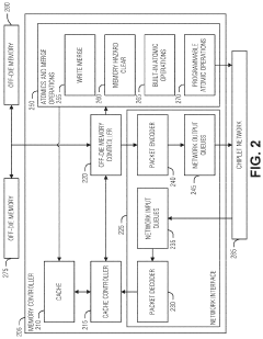
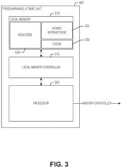
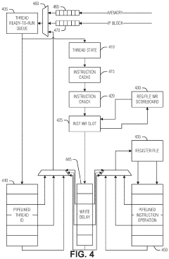
Innovative Chiplet Interconnect Technologies
Variable pipeline length in a barrel-multithreaded processor
PatentActiveUS11847464B2
Innovation
- Implementing a variable pipeline length in processors to allow instructions to complete and writeback early, and using a scoreboard to detect and manage register writeback conflicts, ensuring efficient thread rescheduling and minimizing idle cycles.
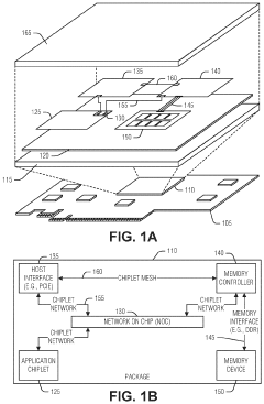
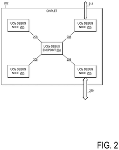
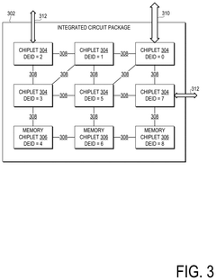
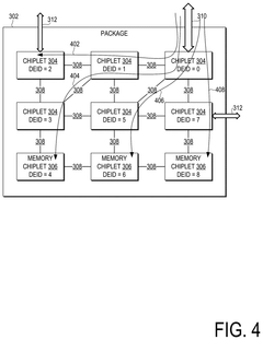
Technologies for a unified test and debug architecture
PatentPendingUS20240329129A1
Innovation
- A unified test and debug architecture is implemented using an external hardware debug interface that supports multiple protocols, including UCIe, JTAG, I2C, and PCIe, allowing debug messages to be sent and routed through a package with multiple chiplets, enabling interoperable debug/test solutions and facilitating infield debugging.
Chiplet Standards and Interoperability
The advancement of chiplet technology has necessitated the development of robust standards and interoperability protocols to ensure seamless integration and communication between different chiplet components. These standards are crucial for enabling the widespread adoption of chiplet-based designs across the semiconductor industry.
One of the most prominent initiatives in this area is the Universal Chiplet Interconnect Express (UCIe) standard. UCIe aims to establish a common interconnect framework for chiplets, allowing for interoperability between chiplets from different manufacturers. This standard defines both the physical and protocol layers for die-to-die interconnects, facilitating high-bandwidth, low-latency communication between chiplets.
Another significant standard is the Advanced Interface Bus (AIB), developed by Intel. AIB provides a standardized interface for connecting chiplets, offering high-speed data transfer and power efficiency. It has been adopted by several industry players and is compatible with various packaging technologies.
The Open Compute Project (OCP) has also contributed to chiplet standardization efforts through its Open Domain-Specific Architecture (ODSA) subproject. ODSA focuses on creating open standards for chiplet-based designs, including specifications for physical interfaces, protocols, and security features.
Interoperability between chiplets is further enhanced by the development of standard protocols for data transfer and communication. Examples include the Bunch of Wires (BoW) interface, which provides a simple and cost-effective solution for chiplet interconnects, and the High Bandwidth Memory (HBM) standard, which defines a high-performance memory interface often used in chiplet designs.
The adoption of these standards and protocols is crucial for fostering innovation and competition in the chiplet ecosystem. By ensuring interoperability, they enable semiconductor companies to focus on their core competencies while leveraging chiplets from various suppliers. This approach not only reduces development costs but also accelerates time-to-market for new products.
However, challenges remain in achieving full interoperability across all chiplet designs. Different manufacturers may have varying requirements for power, performance, and area (PPA) trade-offs, which can impact the implementation of standardized interfaces. Additionally, ensuring compatibility between chiplets manufactured using different process nodes presents ongoing technical challenges.
As the chiplet ecosystem continues to evolve, ongoing collaboration between industry stakeholders, standards organizations, and research institutions will be essential for refining existing standards and developing new ones to address emerging challenges. This collaborative effort will be crucial in realizing the full potential of chiplet technology and driving further advancements in integrated circuit design.
Economic Impact of Chiplet Adoption
The adoption of chiplet technology is poised to have a significant economic impact on the integrated circuit (IC) industry. This innovative approach to chip design and manufacturing offers substantial cost savings and improved production efficiency, which are crucial factors in the highly competitive semiconductor market.
One of the primary economic benefits of chiplet adoption is the potential for reduced manufacturing costs. By breaking down complex system-on-chip (SoC) designs into smaller, modular components, chipmakers can leverage more mature and cost-effective manufacturing processes for certain parts of the chip. This strategy allows companies to optimize production costs by using the most appropriate process node for each chiplet, rather than being forced to manufacture the entire chip using the latest and most expensive technology.
Furthermore, chiplet technology enables improved yield rates in semiconductor production. As chip sizes increase and process nodes shrink, the likelihood of defects occurring during manufacturing also rises. By producing smaller chiplets separately and then integrating them, manufacturers can significantly reduce the impact of defects on overall chip yield. This improvement in yield translates directly to cost savings and increased profitability for semiconductor companies.
The modular nature of chiplets also facilitates more flexible product development and customization. Companies can mix and match different chiplets to create a wide range of products tailored to specific market segments or customer requirements. This flexibility allows for faster time-to-market and more efficient use of research and development resources, potentially leading to increased revenue streams and market share.
Chiplet technology is expected to drive innovation and competition within the semiconductor industry. As the barriers to entry for designing complex chips are lowered, smaller companies and startups may be able to enter the market with innovative designs, fostering a more diverse and competitive ecosystem. This increased competition could lead to accelerated technological advancements and potentially lower prices for end consumers.
The adoption of chiplets is also likely to impact the semiconductor supply chain. As the industry shifts towards more modular chip designs, new opportunities may arise for specialized chiplet manufacturers and packaging companies. This could lead to a more distributed and resilient supply chain, potentially reducing the industry's vulnerability to disruptions and geopolitical tensions.
In conclusion, the economic impact of chiplet adoption is expected to be far-reaching, affecting manufacturing costs, product development strategies, market dynamics, and industry structure. As this technology continues to mature and gain widespread adoption, it has the potential to reshape the economic landscape of the semiconductor industry and drive significant value creation for companies and consumers alike.
Unlock deeper insights with Patsnap Eureka Quick Research — get a full tech report to explore trends and direct your research. Try now!
Generate Your Research Report Instantly with AI Agent
Supercharge your innovation with Patsnap Eureka AI Agent Platform!