

How Do GaN HEMTs Compare With Superjunction MOSFETs?
SEP 8, 20259 MIN READ
Generate Your Research Report Instantly with AI Agent
PatSnap Eureka helps you evaluate technical feasibility & market potential.
GaN HEMT and SJ MOSFET Technology Evolution
The evolution of power semiconductor technologies has witnessed significant advancements over the past few decades, with Gallium Nitride High Electron Mobility Transistors (GaN HEMTs) and Superjunction Metal-Oxide-Semiconductor Field-Effect Transistors (SJ MOSFETs) emerging as pivotal innovations in power electronics.
SJ MOSFET technology originated in the late 1990s as an enhancement to conventional silicon MOSFETs. The breakthrough came with the introduction of alternating p-type and n-type vertical columns in the drift region, enabling devices to maintain high blocking voltage while significantly reducing on-resistance. This represented a fundamental shift from the traditional planar structure, allowing SJ MOSFETs to overcome the silicon limit line.
The commercial deployment of SJ MOSFETs began in the early 2000s, with companies like Infineon (CoolMOS), STMicroelectronics (MDmesh), and ON Semiconductor introducing their respective variants. These devices quickly gained traction in applications requiring 500-900V ratings, offering substantial efficiency improvements over standard MOSFETs.
GaN HEMT technology, meanwhile, has followed a different evolutionary path. Research on GaN as a semiconductor material intensified in the 1990s, primarily driven by defense and telecommunications applications. The unique properties of GaN, including its wide bandgap (3.4 eV compared to silicon's 1.1 eV) and high electron mobility, positioned it as a promising material for high-frequency and high-power applications.
The early 2000s saw significant research milestones in GaN HEMT development, but commercial viability remained challenging due to substrate costs and reliability concerns. A critical turning point came with the development of GaN-on-Silicon technology around 2010, which dramatically reduced manufacturing costs by growing GaN epitaxial layers on standard silicon wafers.
From 2010 to 2015, companies like EPC, Transphorm, GaN Systems, and Navitas began commercializing GaN power devices, focusing initially on lower voltage applications (100-200V). The technology has since matured, with current GaN HEMTs now addressing applications in the 100-650V range with exceptional switching performance.
Recent years have witnessed an acceleration in both technologies' development. SJ MOSFETs have evolved through multiple generations, with each iteration offering improved performance characteristics and reliability. The latest generations feature optimized cell structures and enhanced gate designs, pushing the boundaries of silicon-based performance.
Simultaneously, GaN HEMTs have overcome many early reliability challenges and manufacturing constraints. Integration advancements have led to monolithic GaN power ICs that combine drive and protection functions with the power switch, enabling more compact and efficient power conversion systems.
Looking at the trajectory, SJ MOSFETs represent the pinnacle of silicon-based power devices, while GaN HEMTs exemplify the transition to wide bandgap semiconductor technologies that promise to transcend silicon's fundamental limitations in power electronics applications.
Power Electronics Market Demand Analysis
The power electronics market is experiencing unprecedented growth driven by the increasing demand for energy-efficient solutions across multiple industries. The global power electronics market was valued at approximately $40 billion in 2021 and is projected to reach $63 billion by 2028, growing at a CAGR of around 6.8%. This growth is particularly evident in sectors such as automotive, renewable energy, industrial automation, and consumer electronics.
The automotive sector represents one of the most significant drivers for advanced power semiconductor technologies. With electric vehicles (EVs) gaining market share globally, the demand for high-efficiency power conversion solutions has intensified. The EV market requires power semiconductors capable of handling higher voltages, frequencies, and temperatures while maintaining efficiency above 98% to maximize battery range and reduce cooling requirements.
Renewable energy systems constitute another major market segment driving innovation in power electronics. Solar inverters and wind power converters demand semiconductors with superior switching characteristics to minimize energy losses during DC-AC conversion. The global solar inverter market alone is expected to grow at 8.5% CAGR through 2027, creating substantial demand for next-generation power devices.
Data centers represent a rapidly expanding market for advanced power electronics, with their power consumption increasing by approximately 15% annually. The need for more efficient power supplies and server components has become critical as companies seek to reduce operational costs and meet sustainability goals. This sector particularly values power semiconductors that can reduce conversion losses and operate at higher switching frequencies.
Industrial motor drives account for nearly 30% of global electricity consumption, making them a prime target for efficiency improvements through better power electronics. The industrial automation sector's transition toward more precise motor control and energy recovery systems has created demand for faster switching devices with lower conduction losses.
Consumer electronics manufacturers are increasingly focusing on fast-charging technologies and compact power adapters, driving demand for semiconductors that can operate efficiently at higher power densities. The market for GaN-based fast chargers has grown by over 200% since 2019, demonstrating the commercial viability of wide-bandgap semiconductors in consumer applications.
Regional analysis shows Asia-Pacific dominating the power electronics market with approximately 45% share, followed by North America and Europe. China's aggressive push toward electrification across transportation and industrial sectors has created the world's largest single market for advanced power semiconductors, while European regulations on energy efficiency continue to drive adoption of premium power electronic solutions.
Technical Challenges and Limitations Comparison
GaN HEMTs and Superjunction MOSFETs both face distinct technical challenges that impact their performance and adoption. GaN HEMTs struggle with reliability issues, particularly dynamic RDS(on) degradation under high-voltage stress conditions. This phenomenon, caused by electron trapping in the AlGaN/GaN interface or buffer layers, can increase on-resistance over time, affecting long-term performance stability. Additionally, GaN devices exhibit current collapse under switching conditions, where transient increases in on-resistance occur due to charge trapping effects.
Manufacturing consistency presents another significant challenge for GaN technology. The epitaxial growth process for GaN layers requires precise control to minimize defect density, which directly impacts device performance and yield. Current GaN manufacturing processes also face scalability limitations compared to the mature silicon-based fabrication infrastructure used for Superjunction MOSFETs.
Thermal management remains problematic for GaN HEMTs due to their high power density operation. The concentrated heat generation in smaller die areas necessitates advanced packaging solutions and thermal interface materials to prevent performance degradation and ensure reliability at elevated temperatures.
Superjunction MOSFETs face different technical limitations. Their complex vertical structure with alternating n and p pillars requires multiple epitaxial growth and implantation steps, increasing manufacturing complexity and cost. As devices scale to higher voltage ratings (>900V), maintaining precise charge balance becomes increasingly difficult, limiting further improvements in the figure of merit.
Switching performance in Superjunction MOSFETs is constrained by inherent silicon material properties. Despite structural optimizations, these devices exhibit higher switching losses at frequencies above 100kHz compared to GaN HEMTs. Additionally, their body diode characteristics present reverse recovery issues that limit high-frequency operation in hard-switching applications.
Both technologies face application-specific integration challenges. GaN HEMTs typically require specialized gate drivers due to their lower gate threshold voltages and sensitivity to overvoltage conditions. Their lateral structure also results in higher parasitic inductances that must be carefully managed in circuit design. Superjunction MOSFETs, while compatible with standard silicon gate drivers, face limitations in achieving ultra-compact designs due to their larger die size requirements for equivalent performance.
Cost considerations remain a significant barrier for GaN HEMTs despite their superior technical performance. The manufacturing infrastructure for Superjunction MOSFETs benefits from decades of silicon process optimization and economies of scale, while GaN technology is still evolving toward cost parity, particularly for applications below 650V where the performance advantages may not justify the price premium.
Current Implementation Solutions and Architectures
01 Switching performance comparison between GaN HEMTs and SJ MOSFETs
GaN HEMTs generally demonstrate superior switching performance compared to Superjunction MOSFETs, particularly in high-frequency applications. The faster switching speeds of GaN HEMTs result from their higher electron mobility and smaller gate capacitance. This enables reduced switching losses and allows for operation at higher frequencies, making them advantageous in power conversion applications requiring high efficiency. The performance difference is especially notable in hard-switching topologies where GaN HEMTs can achieve significantly lower turn-on and turn-off losses.- Switching performance comparison between GaN HEMTs and SJ MOSFETs: GaN HEMTs demonstrate superior switching performance compared to Superjunction MOSFETs, particularly in high-frequency applications. The faster switching speeds of GaN HEMTs result in reduced switching losses and higher efficiency. This advantage is attributed to the higher electron mobility and smaller input capacitance of GaN devices, allowing them to operate efficiently at frequencies where SJ MOSFETs experience significant performance degradation.
- Power density and thermal management comparison: GaN HEMTs offer higher power density compared to Superjunction MOSFETs due to their wide bandgap properties and lateral device structure. This allows for smaller device footprints and more compact power systems. However, the higher power density creates thermal management challenges that require innovative cooling solutions. SJ MOSFETs generally have better thermal conductivity through their vertical structure, which can be advantageous in applications where heat dissipation is critical.
- Cost-performance trade-offs between technologies: While GaN HEMTs offer superior performance metrics in terms of switching speed and power density, Superjunction MOSFETs maintain advantages in cost-effectiveness for certain applications. The manufacturing processes for SJ MOSFETs are more mature, resulting in lower production costs. GaN technology typically commands a price premium but delivers performance benefits that can justify the higher cost in applications where efficiency and size are critical factors. The selection between these technologies often involves balancing performance requirements against budget constraints.
- Reliability and robustness comparison: Superjunction MOSFETs generally demonstrate higher robustness in terms of surge capability and short-circuit withstand time compared to GaN HEMTs. The mature silicon technology has well-established reliability data and failure mechanisms. GaN HEMTs are still evolving in terms of reliability characterization, with ongoing improvements in dynamic RDS(on) stability and gate reliability. The different failure modes between these technologies necessitate different protection strategies in circuit design.
- Application-specific performance optimization: The performance comparison between GaN HEMTs and Superjunction MOSFETs varies significantly depending on the application requirements. GaN HEMTs excel in high-frequency, high-efficiency applications such as compact power adapters and telecom power supplies. SJ MOSFETs remain competitive in high-voltage, high-current applications where robustness is prioritized over switching speed. Hybrid solutions incorporating both technologies are emerging to leverage the strengths of each in specific parts of power conversion systems.
02 Thermal performance and reliability comparison
Superjunction MOSFETs typically demonstrate better thermal performance and reliability under high-temperature conditions compared to GaN HEMTs. Silicon-based SJ MOSFETs have more mature packaging technologies and better thermal conductivity, allowing for more efficient heat dissipation. GaN HEMTs, while offering superior electrical performance, often face challenges with thermal management due to higher power density and thermal resistance. This difference in thermal performance impacts the reliability and lifetime of devices in high-power applications, with SJ MOSFETs generally showing advantages in applications with significant thermal stress.Expand Specific Solutions03 Cost-performance trade-offs between technologies
Superjunction MOSFETs offer better cost-performance ratios for many applications due to mature manufacturing processes and established supply chains. GaN HEMTs provide superior electrical performance but at higher production costs. The cost differential impacts adoption in various market segments, with SJ MOSFETs dominating cost-sensitive applications while GaN HEMTs are preferred in high-performance scenarios where efficiency and size advantages justify the premium. As GaN manufacturing technology matures, this cost gap is gradually narrowing, potentially shifting the balance in more application areas.Expand Specific Solutions04 Application-specific performance advantages
The performance advantages of GaN HEMTs and Superjunction MOSFETs vary significantly across different application domains. GaN HEMTs excel in high-frequency power conversion applications such as compact chargers, RF power amplifiers, and high-density power supplies due to their superior switching characteristics. Superjunction MOSFETs remain dominant in high-voltage, high-current applications like industrial motor drives, automotive systems, and grid-connected equipment where robustness and thermal performance are critical. The selection between these technologies depends on specific application requirements including operating frequency, power level, thermal conditions, and system cost constraints.Expand Specific Solutions05 Device structure and material property impacts on performance
The fundamental differences in device structures and material properties between GaN HEMTs and Superjunction MOSFETs significantly impact their performance characteristics. GaN HEMTs utilize a two-dimensional electron gas (2DEG) channel formed at the AlGaN/GaN heterojunction, enabling high electron mobility and reduced on-resistance. Superjunction MOSFETs employ alternating n-type and p-type pillars to achieve charge balance, allowing for higher breakdown voltage while maintaining low on-resistance. These structural differences result in distinct performance profiles, with GaN offering advantages in switching speed and power density, while SJ MOSFETs provide benefits in breakdown voltage capability and avalanche ruggedness.Expand Specific Solutions
Key Manufacturers and Competitive Landscape
The GaN HEMT versus Superjunction MOSFET competitive landscape is currently in a growth phase, with the market expanding rapidly due to increasing demand for high-efficiency power devices in electric vehicles, renewable energy, and data centers. While Superjunction MOSFETs dominate the established $4-5 billion power semiconductor market, GaN HEMTs are gaining momentum with their superior switching speeds and efficiency at higher frequencies. Leading players like Wolfspeed, Infineon, and Texas Instruments are advancing GaN technology, while emerging companies such as Innoscience and Enphase Energy are driving innovation. Research institutions including Xidian University and University of Electronic Science & Technology of China are contributing to technological maturation, though GaN HEMTs still face challenges in cost reduction and reliability improvement before achieving mainstream adoption.
Wolfspeed, Inc.
Technical Solution: Wolfspeed has pioneered SiC-based power devices and is now leveraging this expertise in GaN HEMT technology. Their GaN HEMTs utilize a high electron mobility transistor structure with a two-dimensional electron gas (2DEG) channel formed at the AlGaN/GaN heterojunction interface. This design enables significantly higher electron mobility compared to traditional MOSFETs. Wolfspeed's GaN HEMTs operate at switching frequencies exceeding 100 MHz with minimal switching losses, compared to Superjunction MOSFETs that typically operate optimally below 100 kHz. Their devices achieve breakdown voltages of 650V to 1200V while maintaining lower on-resistance per unit area (Ron*A) than comparable Superjunction MOSFETs. The company's latest generation demonstrates a figure of merit (Ron*Qg) improvement of approximately 10x over silicon-based alternatives[1][3].
Strengths: Superior switching performance with significantly lower switching losses at high frequencies; smaller die size for equivalent current ratings; better thermal performance allowing operation at higher junction temperatures. Weaknesses: Higher cost compared to silicon Superjunction MOSFETs; requires more complex gate drive circuits; less robust against overvoltage conditions.
Infineon Technologies Austria AG
Technical Solution: Infineon has developed CoolGaN™ technology, an enhancement-mode (e-mode) GaN HEMT platform that addresses the gate drive complexity issues of traditional depletion-mode GaN devices. Their p-GaN gate technology creates normally-off devices that are compatible with standard MOSFET drivers while maintaining GaN's inherent performance benefits. Infineon's 600V CoolGaN™ HEMTs achieve an RDS(on) as low as 55mΩ in standard packages, with switching speeds up to 10x faster than Superjunction MOSFETs. Their devices demonstrate a hard-switching figure of merit (RDS(on) × Qoss) approximately 5x better than silicon Superjunction alternatives, enabling power density improvements of 40-50% in typical applications. Infineon has also addressed reliability concerns through extensive qualification testing, demonstrating stable performance after 1000 hours of HTOL (High Temperature Operating Life) testing at 150°C[2][5].
Strengths: Normally-off operation compatible with standard gate drivers; excellent hard-switching performance; comprehensive reliability testing and qualification; established supply chain and manufacturing infrastructure. Weaknesses: Higher cost structure than silicon alternatives; limited voltage ratings compared to SiC options; thermal management challenges in high-power applications.
Critical Performance Parameters and Benchmarking
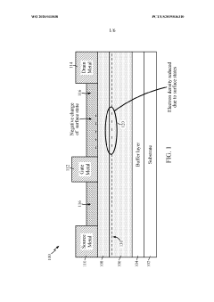
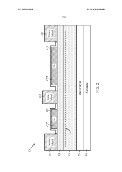
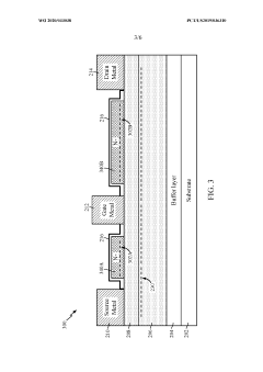
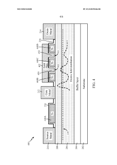
Gallium nitride high electron mobility transistor with ledges and field plates
PatentWO2020033038A1
Innovation
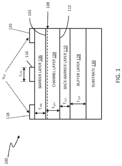
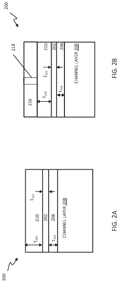
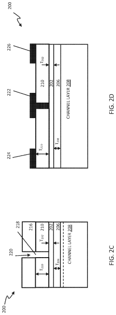
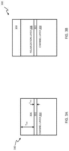
- Incorporating n-doped protuberances, or ledges, between the gate and source/drain electrodes, and optionally using field plates, to reduce surface states and increase channel electron density, thereby enhancing breakdown voltage and switching efficiency.
HIGH ELECTRON MOBILITY TRANSISTORS (HEMTS) INCLUDING A YTTRIUM (Y) AND ALUMINUM NITRIDE (AlN) (YAlN) ALLOY LAYER
PatentActiveUS20230223467A1
Innovation
- Incorporating a lattice-matched yttrium aluminum nitride (YAlN) alloy as a back-barrier layer in HEMTs, which has a wider bandgap than the gallium nitride channel layer, preventing secondary 2DEG formation and reducing thermal resistance, and can be used as an etch stop layer to improve electron confinement and gate control.
Thermal Management and Reliability Assessment
Thermal management represents a critical differentiating factor between GaN HEMTs and Superjunction MOSFETs. GaN HEMTs operate at higher junction temperatures (typically up to 175°C) compared to Si-based Superjunction MOSFETs (limited to around 150°C). This temperature advantage stems from GaN's wider bandgap properties, allowing devices to function reliably at elevated temperatures where silicon-based devices would experience thermal runaway.
Despite this theoretical advantage, GaN HEMTs face unique thermal challenges. Their smaller die size results in higher power density, creating localized hotspots that require sophisticated thermal management solutions. The thermal conductivity of GaN (130 W/mK) is lower than silicon (150 W/mK), necessitating advanced packaging technologies to efficiently dissipate heat.
Reliability assessment protocols differ significantly between these technologies. Superjunction MOSFETs benefit from decades of silicon reliability data and established qualification procedures. In contrast, GaN HEMTs require new reliability models that account for unique failure mechanisms such as current collapse, dynamic RON degradation, and gate leakage issues under high-temperature operation.
Accelerated life testing reveals that GaN HEMTs demonstrate excellent performance under high-temperature reverse bias (HTRB) conditions, often exceeding silicon devices. However, they may exhibit greater sensitivity to humidity and environmental contaminants, requiring hermetic packaging solutions in certain applications.
Mean Time Between Failure (MTBF) calculations indicate comparable or superior long-term reliability for GaN HEMTs in properly designed systems. Field data from early GaN power applications shows promising reliability metrics, with failure rates approaching those of mature silicon technologies despite being relatively new to market.
Thermal cycling performance presents another distinction. Superjunction MOSFETs typically utilize wire bonding that can be susceptible to fatigue during thermal cycling. GaN HEMTs increasingly employ advanced packaging techniques like copper clip bonding or direct die attach methods that demonstrate superior thermal cycling resilience.
System-level thermal management strategies must be adapted when transitioning from Superjunction MOSFETs to GaN HEMTs. The faster switching speeds of GaN generate heat transients that require more responsive cooling solutions. Additionally, the smaller parasitic capacitances in GaN devices reduce switching losses but can shift thermal management priorities toward conduction losses and gate driver circuits.
Cost-Performance Trade-offs and Economic Viability
When evaluating GaN HEMTs against Superjunction MOSFETs, cost considerations remain a critical factor influencing adoption rates across different market segments. Currently, GaN HEMTs command a significant price premium, typically 2-3 times higher than equivalent Superjunction MOSFETs. This price differential stems primarily from lower production volumes, specialized manufacturing processes, and ongoing research and development investments in GaN technology.
The economic viability assessment must consider total system costs rather than merely component pricing. While GaN HEMTs require higher initial investment, they enable smaller passive components, reduced cooling requirements, and more compact designs. These advantages can offset the higher semiconductor costs by reducing overall bill of materials and manufacturing expenses. For high-frequency applications above 100 kHz, the system-level cost benefits of GaN often outweigh the component price premium.
Performance-to-cost ratio calculations reveal interesting market segmentation patterns. In high-end applications where efficiency and power density are paramount—such as data center power supplies, electric vehicle chargers, and aerospace systems—GaN HEMTs demonstrate compelling economic value despite higher unit costs. The performance advantages translate directly into operational savings through reduced energy consumption, which can yield return on investment within 1-3 years depending on usage patterns.
Conversely, in cost-sensitive consumer electronics and industrial applications with moderate performance requirements, Superjunction MOSFETs maintain stronger economic positioning. Their mature supply chain, established reliability data, and competitive pricing create barriers to GaN adoption in these segments. Market analysis indicates that GaN must achieve approximately 30-40% cost reduction to penetrate these price-sensitive markets effectively.
Manufacturing economies of scale represent the primary pathway toward cost parity. As GaN production volumes increase, particularly with the transition to 8-inch wafers and improved yield rates, industry analysts project a 15-20% annual cost reduction trajectory. This suggests potential price convergence with high-end Superjunction devices within 4-5 years, though complete cost parity across all power ratings remains a longer-term prospect.
The economic equation is further influenced by regulatory factors. As energy efficiency standards become more stringent globally, the performance advantages of GaN translate into compliance benefits that can justify higher component costs. This regulatory-driven value proposition is particularly evident in power supplies, motor drives, and renewable energy applications where efficiency requirements continue to tighten.
Unlock deeper insights with PatSnap Eureka Quick Research — get a full tech report to explore trends and direct your research. Try now!
Generate Your Research Report Instantly with AI Agent
Supercharge your innovation with PatSnap Eureka AI Agent Platform!