How Do Resistive RAM Developments Affect Market Regulations?
OCT 9, 202510 MIN READ
Generate Your Research Report Instantly with AI Agent
PatSnap Eureka helps you evaluate technical feasibility & market potential.
ReRAM Technology Evolution and Objectives
Resistive Random Access Memory (ReRAM) has evolved significantly since its conceptual introduction in the 1960s. The technology gained substantial research momentum in the early 2000s when limitations of conventional memory technologies became increasingly apparent. ReRAM represents a promising non-volatile memory solution that offers advantages in power consumption, switching speed, and scalability compared to traditional flash memory technologies.
The evolution of ReRAM technology has been characterized by several key milestones. Initially, metal oxide-based ReRAM structures demonstrated the fundamental switching mechanism. Subsequently, researchers focused on improving reliability, endurance, and retention characteristics through material engineering and device architecture optimization. Recent advancements have centered on multi-level cell capabilities, 3D integration, and neuromorphic computing applications, expanding ReRAM's potential beyond conventional memory applications.
The primary objective of ReRAM development is to establish a commercially viable alternative to existing memory technologies that can address the growing demands of data-intensive applications. This includes achieving higher density, lower power consumption, faster operation, and improved reliability at competitive cost structures. Additionally, ReRAM aims to bridge the performance gap between storage and computing, potentially enabling in-memory computing paradigms that could revolutionize data processing architectures.
From a regulatory perspective, ReRAM development intersects with several critical areas of market governance. As this technology matures toward mass production, regulatory frameworks must adapt to address novel manufacturing processes, materials usage, and potential environmental impacts. The unique properties of ReRAM, particularly its non-volatile nature and potential for radiation hardness, also raise considerations for data security standards and critical infrastructure applications.
The trajectory of ReRAM technology suggests several regulatory challenges on the horizon. First, as ReRAM moves into consumer electronics, regulations regarding data retention, security, and privacy will need reassessment. Second, the specialized materials used in ReRAM fabrication may require updates to supply chain regulations and environmental compliance standards. Finally, as ReRAM enables new computing architectures, regulatory frameworks for intellectual property protection and technology export controls may require significant revision.
The convergence of ReRAM technology with artificial intelligence applications presents additional regulatory considerations. As ReRAM-based neuromorphic systems potentially enable more efficient AI processing at the edge, questions regarding autonomous decision-making, data sovereignty, and algorithmic transparency become increasingly relevant to market regulation frameworks.
Market Demand Analysis for ReRAM Solutions
The global market for Resistive Random Access Memory (ReRAM) solutions is experiencing significant growth, driven by increasing demand for high-performance, energy-efficient memory technologies. Current market projections indicate that the ReRAM market is expected to grow at a compound annual growth rate of 16% through 2028, with particularly strong demand emerging from data centers, IoT applications, and artificial intelligence systems.
The primary market demand for ReRAM stems from its unique value proposition compared to traditional memory technologies. ReRAM offers non-volatility, high endurance, fast switching speeds, and low power consumption - characteristics that address critical pain points in existing memory hierarchies. Enterprise data centers represent the largest market segment, where ReRAM's ability to reduce power consumption while maintaining performance creates compelling total cost of ownership advantages.
Consumer electronics manufacturers are increasingly exploring ReRAM integration for next-generation mobile devices, wearables, and smart home products. This segment values ReRAM's potential to extend battery life while enabling faster data access. Market research indicates that approximately 30% of smartphone manufacturers are evaluating ReRAM for future product generations, signaling growing mainstream interest.
The automotive sector presents another substantial growth opportunity, particularly for advanced driver-assistance systems (ADAS) and autonomous vehicles. These applications require memory solutions that can withstand extreme temperatures and offer radiation hardness - areas where ReRAM demonstrates superior characteristics compared to flash memory alternatives.
Industrial IoT applications represent a rapidly expanding market segment for ReRAM solutions. The technology's ability to operate in harsh environments while consuming minimal power aligns perfectly with the requirements of remote sensors and edge computing devices. Market analysis shows industrial automation companies are increasingly specifying ReRAM in their product roadmaps.
Healthcare and medical device manufacturers are emerging as significant potential customers, driven by ReRAM's reliability and radiation resistance. Applications range from implantable medical devices to portable diagnostic equipment, where memory failure is unacceptable and power efficiency is critical.
Market adoption faces several challenges, including cost premiums compared to established technologies, manufacturing scalability concerns, and integration complexities with existing systems. However, as production volumes increase and manufacturing processes mature, the cost differential is expected to narrow significantly over the next three years.
Customer surveys indicate that reliability, power efficiency, and cost are the three most important factors influencing purchasing decisions for memory solutions. ReRAM's performance in the first two categories positions it favorably, while ongoing development efforts focus on addressing cost concerns through manufacturing optimization and economies of scale.
ReRAM Development Status and Technical Barriers
Resistive RAM (ReRAM) technology has reached a critical development stage with significant market implications. Current global development status shows varying levels of maturity across regions, with the United States, South Korea, Japan, and China leading research efforts. Major semiconductor companies including Samsung, Micron, Intel, and emerging players like Weebit Nano and Crossbar have achieved notable breakthroughs in recent years, transitioning from laboratory research to commercial production phases.
Despite promising advancements, ReRAM faces substantial technical barriers that impede widespread market adoption. The most significant challenge remains endurance limitations, with current ReRAM cells typically achieving 10^5 to 10^7 write cycles—significantly lower than NAND flash (10^5) but still insufficient for universal memory applications requiring 10^12 or more cycles. This limitation restricts ReRAM's application in high-write environments and creates regulatory concerns regarding product lifetime guarantees.
Retention stability presents another critical barrier, particularly at elevated temperatures. While some ReRAM technologies demonstrate 10-year data retention at room temperature, performance degrades substantially at higher operating temperatures common in industrial and automotive applications. This variability creates challenges for establishing standardized testing protocols and certification requirements across different market segments.
Scaling issues continue to hinder ReRAM development, with sub-20nm nodes exhibiting increased variability in switching behavior and resistance states. This inconsistency complicates the establishment of reliable quality control standards and raises questions about appropriate testing methodologies for regulatory compliance. The semiconductor industry currently lacks consensus on standardized testing protocols specific to ReRAM technology.
Manufacturing integration represents a significant hurdle, as ReRAM requires materials and processes not traditionally used in conventional CMOS fabrication. The introduction of new materials such as hafnium oxide, tantalum oxide, and various transition metal oxides necessitates careful evaluation of environmental and safety regulations. Some of these materials face varying regulatory restrictions across different countries, creating compliance challenges for global supply chains.
Power consumption characteristics of ReRAM present both opportunities and regulatory challenges. While ReRAM offers lower operational power than conventional memory technologies, its switching mechanisms can produce current spikes that may interfere with sensitive electronic systems. This creates potential electromagnetic compatibility (EMC) regulatory concerns, particularly in medical, automotive, and aerospace applications where strict EMC standards apply.
The reliability and predictability of ReRAM behavior under various environmental conditions remain inconsistent, complicating the development of universal safety standards. This variability has delayed the establishment of industry-wide specifications, creating regulatory uncertainty that impacts market development timelines and investment decisions across the memory ecosystem.
Current ReRAM Implementation Approaches
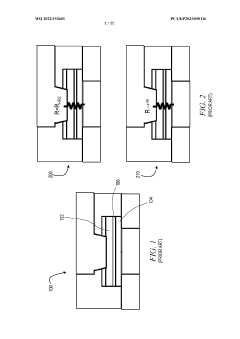
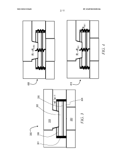
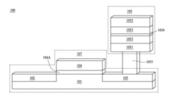
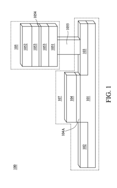
01 Resistive RAM device structures
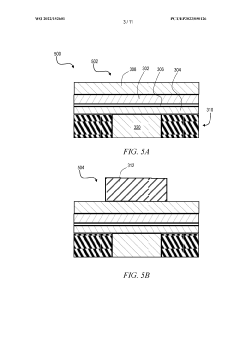
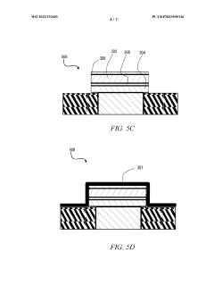
Resistive RAM (RRAM) devices are constructed with specific structures to enable resistive switching behavior. These structures typically include a resistive switching layer sandwiched between two electrodes. Various materials can be used for the resistive switching layer, including metal oxides, chalcogenides, and perovskites. The electrode materials and their interfaces with the switching layer play crucial roles in determining the device performance. Different structural configurations, such as crossbar arrays and 3D stacking, are employed to achieve high-density memory integration.- Resistive RAM device structures: Resistive RAM (RRAM) devices are constructed with specific structural configurations to optimize performance. These structures typically include a resistive switching layer sandwiched between two electrodes. Various materials can be used for the resistive layer, including metal oxides, chalcogenides, and perovskites. The electrode materials and their interfaces with the resistive layer play crucial roles in determining switching characteristics. Advanced structures may incorporate additional layers for improved stability, retention, and endurance.
- Resistive switching mechanisms: The operation of resistive RAM relies on various switching mechanisms that enable transitions between high and low resistance states. These mechanisms include filamentary conduction, where conductive filaments form and rupture within the resistive layer, and interface-type switching, where resistance changes occur at the electrode-oxide interfaces. Other mechanisms involve oxygen vacancy migration, ion movement, or phase changes in the switching material. Understanding these mechanisms is essential for designing reliable RRAM devices with consistent performance characteristics.
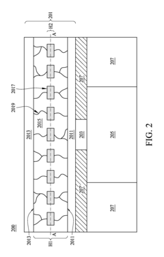
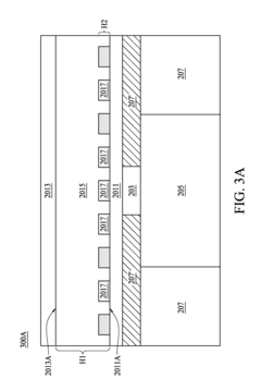
- Memory array architectures: Resistive RAM can be integrated into various memory array architectures to create high-density storage solutions. These architectures include crossbar arrays, where memory cells are placed at the intersections of word and bit lines, and 3D stacked structures that maximize storage density. Circuit designs must address issues such as sneak path currents, which can cause read errors in high-density arrays. Selection devices or transistors are often incorporated to isolate individual memory cells during read and write operations.
- Fabrication methods and materials: The fabrication of resistive RAM involves specific processes and material selections that impact device performance. Common techniques include atomic layer deposition, sputtering, and sol-gel methods for creating the resistive switching layer. Materials engineering focuses on optimizing the composition and structure of the switching layer, which may include doping or creating engineered defects to control switching behavior. Post-deposition treatments such as annealing or electroforming are often employed to initialize the devices and improve their characteristics.
- Integration with CMOS technology: Integrating resistive RAM with conventional CMOS technology is crucial for practical applications. This integration involves addressing challenges related to process compatibility, thermal budgets, and electrical connections between the memory elements and control circuitry. Back-end-of-line integration approaches are commonly used to add RRAM layers above the silicon substrate containing transistors. Design considerations include minimizing parasitic effects, ensuring reliable operation across process variations, and developing appropriate sensing circuits to accurately read the resistance states.
02 Resistive switching mechanisms
The operation of resistive RAM relies on various switching mechanisms that change the resistance state of the memory cell. These mechanisms include filamentary conduction, where conductive filaments form and rupture within the switching layer, and interface-type switching, where the resistance changes at the electrode-oxide interface. Oxygen vacancy migration, ion movement, and phase changes are common physical processes underlying these switching behaviors. Understanding and controlling these mechanisms is essential for improving device reliability, endurance, and retention characteristics.Expand Specific Solutions03 Materials for resistive RAM
The choice of materials significantly impacts the performance of resistive RAM devices. Metal oxides such as HfOx, TaOx, and TiOx are widely used as switching layers due to their compatibility with CMOS processes and good switching characteristics. Two-dimensional materials and novel compounds are being explored to enhance switching speed and reduce power consumption. Electrode materials, including noble metals, transition metals, and conducting oxides, are selected based on their work function, diffusion properties, and chemical stability. Doping and interface engineering are employed to optimize the switching behavior and improve device performance.Expand Specific Solutions04 Integration and fabrication techniques
Fabrication of resistive RAM involves various processing techniques to ensure device reliability and compatibility with existing semiconductor manufacturing processes. These include atomic layer deposition, sputtering, and chemical vapor deposition for thin film growth, along with lithography and etching for pattern definition. Integration challenges such as sneak path issues in crossbar arrays are addressed through selector devices or complementary resistive switches. Back-end-of-line integration enables 3D stacking of memory cells, significantly increasing storage density. Process optimization is crucial to minimize variability and enhance yield.Expand Specific Solutions05 Circuit design and operation
Circuit design for resistive RAM encompasses read/write schemes, sensing amplifiers, and addressing techniques. Pulse programming with carefully controlled voltage amplitude and duration is employed to set and reset the memory states. Current compliance mechanisms prevent device damage during the forming and set operations. Multi-level cell operation, where multiple resistance states are utilized in a single cell, increases storage density. Advanced sensing circuits compensate for device variability and noise. Memory architectures incorporate error correction codes and redundancy schemes to enhance reliability and extend device lifetime.Expand Specific Solutions
Key Industry Players and Competitive Landscape
The Resistive RAM (ReRAM) market is currently in its growth phase, with an estimated market size of $300-500 million and projected to reach $2-3 billion by 2028. The technology is approaching maturity, with key players advancing from research to commercialization stages. Major semiconductor manufacturers like Samsung, TSMC, and Intel are investing heavily in ReRAM development, while specialized companies such as CrossBar and Adesto Technologies are focusing on innovative applications. Asian companies, particularly from Taiwan (Winbond, Macronix) and South Korea (Samsung, KIST), dominate the landscape, with significant research contributions from academic institutions like Peking University and ITRI. Regulatory frameworks are evolving to address data security, power consumption standards, and intellectual property protection as ReRAM increasingly targets IoT, automotive, and AI applications.
KIOXIA Corp.
Technical Solution: KIOXIA (formerly Toshiba Memory) has developed an innovative ReRAM technology platform that builds upon their extensive expertise in flash memory manufacturing. Their approach utilizes tantalum oxide-based switching materials in a filamentary conduction mechanism that provides excellent scalability and performance characteristics. KIOXIA's ReRAM technology demonstrates switching speeds below 10ns, endurance exceeding 10^6 cycles, and retention times projected beyond 10 years at operating temperatures. The company has focused on developing ReRAM as both a storage-class memory solution and as embedded memory for IoT and automotive applications. KIOXIA has implemented advanced error correction and wear-leveling algorithms specifically designed for ReRAM's unique characteristics, addressing regulatory concerns about data integrity and system reliability. Their technology includes built-in security features such as physical unclonable functions (PUFs) and true random number generators (TRNGs) that leverage the inherent stochasticity of ReRAM switching, aligning with emerging cybersecurity regulations. KIOXIA has also pioneered manufacturing techniques that reduce the environmental impact of ReRAM production, anticipating stricter environmental regulations in semiconductor manufacturing.
Strengths: KIOXIA's established position in the memory market provides them with extensive manufacturing expertise and capacity to scale ReRAM production while meeting regulatory quality standards. Their experience navigating flash memory regulations gives them valuable insights for addressing similar challenges with ReRAM. Weaknesses: Their historical focus on consumer electronics may create challenges as they adapt to the more stringent regulatory environments of automotive, medical, and industrial applications where ReRAM has significant potential.
Samsung Electronics Co., Ltd.
Technical Solution: Samsung has pioneered resistive RAM (ReRAM) technology with their comprehensive approach to commercialization. Their technology utilizes metal-oxide based materials (particularly HfO2 and TaOx) in a crossbar architecture that enables high-density storage capabilities. Samsung's ReRAM solutions demonstrate excellent scalability down to sub-10nm nodes, with switching speeds in nanoseconds and power consumption significantly lower than conventional flash memory. The company has developed proprietary selector devices to mitigate sneak path current issues that typically plague high-density ReRAM arrays. Samsung has also implemented multi-level cell capabilities in their ReRAM technology, storing multiple bits per cell to increase memory density without proportional increases in die size. Their integration strategy includes embedding ReRAM directly with logic circuits for in-memory computing applications, which addresses regulatory concerns about data privacy by processing sensitive information locally rather than transmitting it to cloud servers.
Strengths: Samsung's vertical integration allows them to control the entire manufacturing process, ensuring quality control that meets strict regulatory standards. Their established global presence gives them significant influence in shaping industry standards and regulatory frameworks. Weaknesses: The proprietary nature of their technology may create interoperability challenges as regulations increasingly demand standardized approaches to emerging memory technologies.
Critical Patents and Technical Innovations in ReRAM
Setting an upper bound on RRAM resistance
PatentWO2022152601A1
Innovation
- Incorporating a high-resistance semiconductive spacer in parallel with the RRAM module, using materials like TiOxNy or TaxNy, to provide an upper bound on resistance, ensuring proper operation even with manufacturing defects and enhancing stability by encapsulating the filament layer.
Resistive random access memory and manufacturing method thereof
PatentActiveUS20150069315A1
Innovation
- An electric field enhancement layer is introduced to create a higher electric field in specific positions, facilitating predictable and controllable filament formation by depleting oxygen atoms, thereby enhancing the SET and RESET processes of conductive filaments.
Regulatory Framework Impact on ReRAM Adoption
The regulatory landscape surrounding emerging memory technologies like Resistive RAM (ReRAM) is evolving rapidly as these technologies approach widespread commercial adoption. Current regulatory frameworks primarily designed for conventional semiconductor technologies are increasingly challenged by ReRAM's unique characteristics, particularly its non-volatile nature and novel materials composition. Regulatory bodies worldwide are now reassessing existing standards to accommodate these differences.
Data security regulations represent a critical area impacted by ReRAM development. The persistent data storage capability of ReRAM, even during power loss, introduces new considerations for data protection regulations such as GDPR in Europe and CCPA in California. Manufacturers must demonstrate robust security measures that address ReRAM's unique vulnerability profiles, which differ significantly from traditional DRAM or flash memory technologies.
Energy efficiency standards are being reconsidered in light of ReRAM's power consumption characteristics. While ReRAM offers substantial power savings compared to conventional memory technologies, regulatory frameworks designed to measure and certify energy efficiency often lack appropriate benchmarks for these novel technologies. This regulatory gap creates uncertainty for manufacturers seeking to market ReRAM's energy benefits within existing certification programs.
Material composition regulations present another significant challenge. ReRAM typically incorporates materials not commonly used in traditional semiconductor manufacturing, including transition metal oxides and specialized electrode materials. These components may fall under different regulatory scrutiny regarding environmental impact, recyclability, and potential toxicity. Manufacturers must navigate complex compliance requirements across different jurisdictions, often with inconsistent standards.
Intellectual property regulations are experiencing particular strain as ReRAM technology advances. The novel mechanisms underlying ReRAM operation have triggered a surge in patent filings, creating a complex IP landscape that regulatory bodies must monitor to prevent anti-competitive practices. Standard-essential patents for ReRAM technologies are becoming increasingly important as the industry moves toward standardization.
Medical device regulations represent a specialized regulatory domain affected by ReRAM development. The technology's radiation hardness and reliability make it particularly suitable for implantable medical devices, but regulatory approval pathways for such applications remain underdeveloped. Regulatory agencies like the FDA are beginning to consider specific guidance for ReRAM-based medical technologies.
Export control regulations are also evolving in response to ReRAM's strategic importance. As a potentially disruptive technology with applications in sensitive sectors including defense and artificial intelligence, ReRAM development is increasingly subject to national security considerations. Several countries have begun updating their export control lists to specifically address advanced memory technologies including ReRAM.
Data Security and Privacy Implications of ReRAM
The evolution of Resistive Random Access Memory (ReRAM) technology introduces significant data security and privacy implications that warrant careful consideration. As ReRAM devices become increasingly integrated into computing systems, they present unique characteristics that both enhance and challenge existing data protection frameworks.
ReRAM's non-volatile nature means data persists even when power is removed, creating potential vulnerabilities where sensitive information might remain accessible longer than in volatile memory technologies. This persistence characteristic necessitates new approaches to data lifecycle management and secure erasure protocols specifically designed for ReRAM architecture.
The physical properties of ReRAM cells offer inherent security advantages. The resistance-based storage mechanism is less susceptible to electromagnetic side-channel attacks compared to traditional charge-based memories. Additionally, some ReRAM implementations demonstrate resistance to radiation effects, making them suitable for secure applications in harsh environments where data integrity is paramount.
Privacy concerns emerge from ReRAM's potential role in edge computing devices. As these memory solutions enable more sophisticated data processing at the edge, questions arise regarding data localization, consent mechanisms, and transparency in data handling. The ability to process sensitive information locally without transmission to cloud services presents both privacy benefits and regulatory challenges.
ReRAM technologies are increasingly being explored for physical unclonable function (PUF) implementations, which leverage manufacturing variations to create unique device fingerprints. These PUFs can serve as hardware security primitives for device authentication and secure key storage, potentially strengthening privacy-preserving architectures but requiring appropriate regulatory frameworks to govern their implementation.
The integration of ReRAM in neuromorphic computing systems raises additional privacy considerations. These brain-inspired computing architectures may process biometric data and other personally identifiable information in novel ways that existing regulations may not adequately address. The ability of ReRAM-based neuromorphic systems to learn from user behavior patterns creates tension between functionality and privacy preservation.
Regulatory frameworks worldwide are struggling to keep pace with these technological developments. The European Union's General Data Protection Regulation (GDPR), California Consumer Privacy Act (CCPA), and similar legislation must evolve to address ReRAM-specific security properties and vulnerabilities. Industry standards bodies are beginning to develop technical specifications for secure ReRAM implementation, but harmonization with legal requirements remains incomplete.
As ReRAM technologies mature toward mainstream adoption, proactive collaboration between technology developers, privacy advocates, and regulatory authorities will be essential to establish appropriate governance frameworks that balance innovation with robust data protection principles.
Unlock deeper insights with PatSnap Eureka Quick Research — get a full tech report to explore trends and direct your research. Try now!
Generate Your Research Report Instantly with AI Agent
Supercharge your innovation with PatSnap Eureka AI Agent Platform!