How Does Resistive RAM Meet Industry Standards?
OCT 9, 20259 MIN READ
Generate Your Research Report Instantly with AI Agent
Patsnap Eureka helps you evaluate technical feasibility & market potential.
ReRAM Technology Background and Objectives
Resistive Random Access Memory (ReRAM) emerged in the early 2000s as a promising non-volatile memory technology, positioned as a potential successor to flash memory. The technology leverages the fundamental principle of resistance switching, where the application of electrical voltage alters the resistance state of a material, enabling binary data storage. This resistance-based mechanism offers significant advantages in terms of power efficiency, switching speed, and endurance compared to conventional memory technologies.
The evolution of ReRAM technology has been marked by progressive improvements in material science, fabrication techniques, and integration methodologies. Initial research focused primarily on metal oxide-based structures, with subsequent developments exploring various material combinations to enhance performance characteristics. The technology has transitioned from laboratory demonstrations to early commercial implementations, indicating its growing maturity and potential for mainstream adoption.
Industry standards for memory technologies encompass a wide range of performance metrics, including read/write speeds, endurance cycles, retention time, power consumption, and scalability. ReRAM has demonstrated promising capabilities across these parameters, particularly in terms of low power operation and fast switching speeds. However, challenges remain in achieving consistent performance across large arrays and ensuring long-term reliability under various operating conditions.
The primary technical objectives for ReRAM development include enhancing reliability at reduced feature sizes, improving manufacturing yield, and ensuring compatibility with existing semiconductor fabrication processes. Additionally, there is a focused effort to optimize the trade-off between retention time and switching speed, which represents a fundamental challenge for resistance-based memory technologies.
From a standardization perspective, ReRAM must conform to established industry protocols for memory interfaces, reliability testing, and qualification procedures. Organizations such as JEDEC (Joint Electron Device Engineering Council) have been working to develop specific standards for emerging non-volatile memory technologies, including ReRAM, to facilitate broader industry adoption and interoperability.
The trajectory of ReRAM development aligns with the broader industry trend toward more energy-efficient, higher-performance computing architectures. As data-intensive applications continue to proliferate, the demand for memory technologies that can deliver both speed and energy efficiency becomes increasingly critical. ReRAM's potential to serve both as storage and computing elements positions it uniquely within the evolving memory hierarchy.
Looking forward, the technical roadmap for ReRAM includes further miniaturization to sub-10nm nodes, integration with advanced logic processes, and exploration of novel architectures such as crossbar arrays and 3D stacking to maximize density and performance. These developments will be essential for ReRAM to fully meet and exceed industry standards, ultimately enabling its widespread deployment across various computing platforms.
Market Demand Analysis for Non-Volatile Memory
The non-volatile memory market has experienced significant growth in recent years, driven by increasing demand for data storage solutions across various industries. The global non-volatile memory market was valued at approximately $67 billion in 2021 and is projected to reach $125 billion by 2028, growing at a CAGR of around 9.3% during the forecast period. This growth is primarily attributed to the rising adoption of connected devices, IoT applications, and the exponential increase in data generation.
Resistive RAM (ReRAM) is positioned as a promising next-generation non-volatile memory technology that addresses several limitations of existing solutions. The market demand for ReRAM is being fueled by its potential to offer higher density, lower power consumption, and faster operation compared to traditional flash memory. Industries such as automotive, consumer electronics, enterprise storage, and healthcare are showing increasing interest in ReRAM technology.
The automotive sector represents a particularly strong growth area for non-volatile memory, with the increasing integration of advanced driver-assistance systems (ADAS) and autonomous driving features requiring robust, high-performance memory solutions. ReRAM's radiation hardness and temperature stability make it especially suitable for automotive applications, where operating conditions can be harsh.
Consumer electronics continues to be the largest market segment for non-volatile memory, with smartphones, tablets, and wearable devices driving demand. The need for faster boot times, improved application loading, and enhanced user experiences creates opportunities for ReRAM adoption in these devices. Market research indicates that consumers are willing to pay premium prices for devices offering superior performance and responsiveness.
Enterprise storage systems represent another significant market opportunity for ReRAM. Data centers are increasingly seeking memory solutions that can reduce latency, improve energy efficiency, and provide higher endurance. ReRAM's characteristics align well with these requirements, positioning it as a potential replacement for NAND flash in certain storage tiers.
The healthcare and medical devices sector is emerging as a promising market for ReRAM, with applications in implantable devices, patient monitoring systems, and medical imaging equipment. The reliability, low power consumption, and non-volatility of ReRAM make it suitable for critical medical applications where data integrity and device longevity are paramount.
Geographic analysis reveals that North America and Asia-Pacific currently dominate the non-volatile memory market, with China, South Korea, and Taiwan being key manufacturing hubs. However, emerging economies in Southeast Asia and Latin America are showing increasing demand for non-volatile memory solutions as their digital infrastructure expands and smartphone penetration increases.
ReRAM Development Status and Technical Challenges
Resistive RAM (ReRAM) technology has reached a critical juncture in its development cycle, with significant advancements achieved alongside persistent technical challenges. Currently, ReRAM exists in a state of transition from research laboratories to commercial production, with several companies having released initial products while others continue to refine their manufacturing processes.
The global development status of ReRAM shows regional variations in focus and progress. Asian manufacturers, particularly in Japan, South Korea, and Taiwan, have made substantial investments in ReRAM technology, with companies like Panasonic, Samsung, and TSMC leading development efforts. In the United States, companies such as Crossbar, Weebit Nano, and Intel have established strong research programs and patent portfolios in this domain.
Despite promising progress, ReRAM faces several critical technical challenges that impede widespread adoption. Endurance limitations remain a significant concern, with many ReRAM cells demonstrating degradation after 10^6 to 10^9 write cycles—falling short of NAND flash in some applications and significantly below DRAM and SRAM requirements for memory replacement scenarios.
Retention stability presents another major hurdle, particularly at elevated temperatures common in industrial and automotive applications. Current ReRAM technologies struggle to maintain data integrity beyond 10 years at 85°C, which fails to meet the stringent requirements for mission-critical systems and automotive applications that demand 15+ years of data retention.
Variability between cells and across manufacturing batches continues to challenge manufacturers, resulting in inconsistent switching behavior, resistance states, and overall performance metrics. This variability complicates circuit design and necessitates complex error correction mechanisms that increase system complexity and power consumption.
Scaling ReRAM to advanced technology nodes below 28nm introduces additional complications related to current density, heat dissipation, and material interface effects. As cell dimensions shrink, maintaining reliable switching behavior becomes increasingly difficult, requiring innovations in materials science and device architecture.
Power consumption during write operations remains higher than ideal for many low-power applications, particularly in IoT and edge computing scenarios where energy efficiency is paramount. While read operations are relatively efficient, the write energy requirements limit ReRAM's applicability in ultra-low-power devices.
Integration challenges with standard CMOS processes represent another significant barrier, as specialized materials and processing steps for ReRAM fabrication often require modifications to established semiconductor manufacturing flows, increasing production complexity and costs.
Current ReRAM Compliance Solutions
01 Standardization of Resistive RAM Manufacturing Processes
Industry standards for manufacturing processes of Resistive RAM (RRAM) focus on establishing consistent fabrication methods to ensure reliability and performance. These standards address critical aspects such as material selection, deposition techniques, and quality control measures. Standardized manufacturing processes help in achieving uniform device characteristics across different production batches and facilities, which is essential for mass production and commercial viability of RRAM technology.- Standardization of RRAM manufacturing processes: Industry standards for resistive RAM manufacturing focus on establishing consistent fabrication methods, material specifications, and quality control procedures. These standards ensure compatibility across different manufacturing facilities and improve yield rates. Standardized processes include electrode material selection, resistive layer deposition techniques, and integration with CMOS technology. These manufacturing standards help reduce production costs and increase reliability of RRAM devices.
- RRAM device performance and testing standards: Performance standards for resistive RAM define the metrics and testing methodologies used to evaluate device characteristics. These include specifications for switching speed, endurance, retention time, and power consumption. Standardized testing protocols ensure consistent measurement of parameters such as SET/RESET voltages, resistance ratios, and read/write cycles. These standards enable fair comparison between different RRAM technologies and help establish minimum performance requirements for commercial applications.
- RRAM interface and compatibility standards: Interface standards for resistive RAM define how these memory devices communicate with other system components. These standards specify signal protocols, timing requirements, and physical connections to ensure interoperability with existing memory controllers and processors. Standardized interfaces allow RRAM to be integrated into various computing architectures while maintaining backward compatibility with established memory technologies. These standards facilitate the adoption of RRAM in diverse applications from embedded systems to data centers.
- RRAM reliability and endurance standards: Reliability standards for resistive RAM establish the requirements for long-term operation and failure rates. These standards define acceptable limits for data retention, read disturbance immunity, and environmental tolerance (temperature, humidity, radiation). Testing methodologies for accelerated aging and stress conditions help predict device lifetime under normal operating conditions. Standardized reliability metrics enable manufacturers to provide consistent warranty terms and help system designers properly incorporate RRAM into products with specific longevity requirements.
- RRAM design and architecture standards: Design standards for resistive RAM specify the architectural frameworks, cell structures, and array organizations that optimize memory performance and density. These standards define best practices for crossbar array configurations, selector device integration, and addressing schemes. Standardized design rules help manage issues like sneak path currents and read/write disturbances in high-density arrays. These architectural standards facilitate the development of design tools and IP blocks that can be used across the industry to accelerate RRAM adoption.
02 RRAM Device Architecture and Design Standards
Standards related to RRAM device architecture and design focus on establishing specifications for cell structure, array organization, and integration with peripheral circuits. These standards define parameters such as cell size, electrode materials, switching layer composition, and interconnect requirements. Standardized design approaches enable compatibility between different RRAM products and facilitate integration with existing semiconductor technologies, allowing for easier adoption in various applications.Expand Specific Solutions03 Testing and Reliability Standards for RRAM
Industry standards for testing and reliability assessment of RRAM devices establish uniform methods for evaluating performance metrics such as endurance, retention, and switching characteristics. These standards define test conditions, measurement protocols, and acceptance criteria to ensure consistent evaluation across the industry. Standardized reliability testing is crucial for qualifying RRAM technology for different applications, particularly those requiring long-term stability and predictable behavior under various operating conditions.Expand Specific Solutions04 Interface and Communication Standards for RRAM Systems
Standards for RRAM interfaces and communication protocols define how these memory devices interact with other system components. These standards specify signal timing, voltage levels, command structures, and data transfer protocols. Standardized interfaces ensure interoperability between RRAM devices from different manufacturers and facilitate integration with existing memory controllers and systems, enabling seamless adoption of RRAM technology in various computing platforms.Expand Specific Solutions05 RRAM Application-Specific Standards
Application-specific standards for RRAM address requirements for particular use cases such as embedded systems, IoT devices, and data centers. These standards define performance parameters, power consumption limits, form factors, and environmental specifications tailored to specific application domains. By establishing application-specific standards, the industry ensures that RRAM technology can be effectively deployed across diverse scenarios while meeting the unique requirements of each application space.Expand Specific Solutions
Key Industry Players in ReRAM Development
Resistive RAM (RRAM) technology is currently in a transitional phase from research to early commercialization, with the market expected to grow significantly as applications in IoT, AI, and edge computing expand. Major semiconductor players including Samsung, TSMC, SK hynix, and IBM are actively developing RRAM solutions that meet industry standards for reliability, endurance, and retention. Asian manufacturers, particularly from Taiwan and South Korea, dominate the competitive landscape, with companies like Macronix, Winbond, and KIOXIA leading specialized memory development. Research institutions such as ITRI and universities collaborate with industry to address technical challenges in scaling, uniformity, and integration with CMOS processes, ensuring RRAM technologies comply with JEDEC and other international standards for next-generation non-volatile memory applications.
Samsung Electronics Co., Ltd.
Technical Solution: Samsung has developed advanced RRAM technology that utilizes a cross-point array structure with metal-oxide switching materials. Their approach incorporates hafnium oxide-based resistive switching layers that demonstrate excellent endurance (>10^6 cycles) and retention characteristics (>10 years at 85°C). Samsung's RRAM technology meets JEDEC standards for non-volatile memory reliability and has been integrated into their embedded memory solutions. The company has implemented innovative selector devices to minimize sneak path currents, which has been a significant challenge in high-density RRAM arrays. Samsung has also developed specialized programming algorithms that ensure consistent resistance states across large arrays, addressing one of the key requirements for commercial viability.
Strengths: Industry-leading manufacturing capabilities, established supply chain integration, and compatibility with existing CMOS processes. Samsung's vertical integration allows for optimized system-level implementation. Weaknesses: Higher power consumption compared to some competing technologies and challenges with resistance drift over extended operation periods.
International Business Machines Corp.
Technical Solution: IBM has developed phase-change memory (PCM) and RRAM technologies that meet industry standards through their innovative materials engineering approach. Their RRAM technology utilizes metal oxide switching materials with precisely engineered oxygen vacancy profiles that enhance switching reliability and endurance. IBM's RRAM technology complies with JEDEC's data retention standards (10 years at 85°C) while offering multi-level cell capabilities. The company has implemented specialized programming schemes that use adaptive pulse sequences to optimize the trade-off between programming speed and reliability. IBM has also developed comprehensive reliability models that account for various failure mechanisms in RRAM, including retention loss, endurance degradation, and read disturb, enabling accurate lifetime predictions under various operating conditions.
Strengths: Strong integration with AI and high-performance computing systems, excellent research capabilities in materials science, and advanced modeling techniques for reliability prediction. Weaknesses: Less established manufacturing infrastructure compared to memory-focused competitors and challenges with resistance drift that require sophisticated compensation techniques.
Critical Patents and Technical Literature in ReRAM
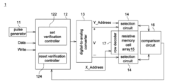
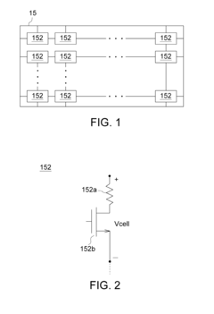
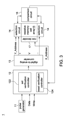
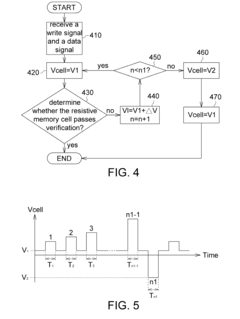
Resistive random access memory and verifying method thereof
PatentActiveUS8300449B2
Innovation
- The implementation of a resistive random access memory (RRAM) system that includes a resistive memory cell, a digital-to-analog converter, a decision logic, and a selection circuit, which applies a reverse voltage to the resistive memory cell during verification failures, utilizing a reference voltage and voltage pulses to enhance the verification process.
Industry Standards and Certification Requirements
Resistive RAM (ReRAM) technology must adhere to rigorous industry standards to ensure reliability, performance, and compatibility across various applications. The Joint Electron Device Engineering Council (JEDEC) has established specific standards for non-volatile memory technologies, including ReRAM, covering aspects such as endurance, retention time, and operational parameters. These standards ensure that ReRAM devices can withstand a minimum of 10^5 to 10^6 write cycles and maintain data integrity for at least 10 years under normal operating conditions.
The International Electrotechnical Commission (IEC) provides additional standards focusing on the electrical characteristics and testing methodologies for emerging memory technologies. For ReRAM to be commercially viable, it must comply with IEC 62830 series standards, which address reliability assessment and qualification procedures for integrated circuit memory devices.
From a manufacturing perspective, ReRAM must meet the International Organization for Standardization (ISO) requirements, particularly ISO 9001 for quality management systems and ISO 14001 for environmental management. These certifications are crucial for semiconductor manufacturers to demonstrate their commitment to quality and environmental responsibility in ReRAM production processes.
The Semiconductor Equipment and Materials International (SEMI) organization has developed standards specifically for wafer fabrication and materials used in semiconductor manufacturing, which directly impact ReRAM production. SEMI standards F47 and F42 address voltage sag immunity and electrostatic discharge (ESD) protection, respectively, both critical for ReRAM reliability.
Military and aerospace applications require ReRAM to meet more stringent standards, such as MIL-STD-883 for microelectronic devices and NASA's EEE-INST-002 for electronic parts selection. These standards impose additional requirements for radiation hardness, temperature range operation, and reliability under extreme conditions.
For consumer electronics and automotive applications, ReRAM must comply with Automotive Electronics Council (AEC) Q100 standards for integrated circuits in automotive applications, ensuring functionality under harsh environmental conditions. Additionally, the European Union's Restriction of Hazardous Substances (RoHS) and Registration, Evaluation, Authorization, and Restriction of Chemicals (REACH) regulations mandate that ReRAM manufacturing processes and materials meet specific environmental and health safety requirements.
Certification processes for ReRAM typically involve third-party testing laboratories that verify compliance with these standards through rigorous testing protocols, including accelerated life testing, environmental stress screening, and reliability demonstration testing. These certifications are essential for market acceptance and integration into commercial products across various industries.
ReRAM Reliability and Endurance Testing Methodologies
Reliability and endurance testing of Resistive RAM (ReRAM) follows rigorous methodologies to ensure compliance with industry standards. These testing protocols typically begin with accelerated stress tests that subject ReRAM cells to conditions exceeding normal operational parameters. Such tests include high-temperature operating life (HTOL) testing, where devices operate at elevated temperatures (typically 85-125°C) for extended periods, and temperature cycling tests that evaluate performance across extreme temperature variations.
Write endurance testing constitutes a critical component of ReRAM qualification, measuring the number of write cycles a cell can withstand before failure. Industry standards generally require ReRAM to achieve 10^5 to 10^7 write cycles, depending on the application domain. Testing involves repeated programming and erasing operations until failure occurs or a predetermined cycle count is reached, with data retention verified at regular intervals.
Data retention testing evaluates how long ReRAM cells can maintain stored information without power. Standard methodologies include baking devices at elevated temperatures (typically 85-125°C) for periods ranging from 168 hours to 1000 hours, followed by verification of data integrity. The Arrhenius equation is commonly applied to extrapolate high-temperature results to normal operating conditions, with 10-year data retention at 85°C being a common industry benchmark.
Statistical analysis plays a vital role in ReRAM testing methodologies. Weibull distribution models are frequently employed to analyze failure rates and predict device lifetimes. Additionally, bit error rate (BER) measurements track the percentage of bits that fail during endurance cycling, with error correction code (ECC) capabilities factored into acceptable failure thresholds.
Standardized test equipment and procedures ensure consistency across the industry. Automated test equipment (ATE) platforms with specialized ReRAM test modules perform precise current and voltage measurements at nanosecond timescales. These systems typically incorporate environmental chambers for temperature control during testing. Test patterns follow JEDEC standards (JESD22-A108, JESD22-A110) for non-volatile memory qualification.
Cross-platform compatibility testing verifies ReRAM functionality across different controller architectures and operating systems. This includes evaluating read/write performance, power consumption profiles, and error rates under various workloads. Industry consortia like JEDEC and IEEE have developed specific test methodologies for emerging non-volatile memories, providing standardized frameworks for ReRAM qualification and certification.
Unlock deeper insights with Patsnap Eureka Quick Research — get a full tech report to explore trends and direct your research. Try now!
Generate Your Research Report Instantly with AI Agent
Supercharge your innovation with Patsnap Eureka AI Agent Platform!