How IGZO Thin Film Enhances Semiconductor Efficiency
SEP 28, 20259 MIN READ
Generate Your Research Report Instantly with AI Agent
PatSnap Eureka helps you evaluate technical feasibility & market potential.
IGZO Technology Background and Objectives
Indium Gallium Zinc Oxide (IGZO) technology represents a significant advancement in semiconductor materials, emerging in the early 2000s as a promising alternative to conventional amorphous silicon (a-Si) and polycrystalline silicon (poly-Si) in thin-film transistor (TFT) applications. Initially developed through collaborative research between Japanese institutions and corporations, IGZO combines the electrical properties of indium, gallium, and zinc oxides to create a semiconductor material with exceptional electron mobility characteristics.
The evolution of IGZO technology has been driven by increasing demands for higher performance displays and more energy-efficient electronic devices. Traditional a-Si TFTs, while cost-effective, suffer from limited electron mobility (typically 0.5-1 cm²/Vs), restricting their application in high-resolution displays and advanced electronic circuits. IGZO emerged as a revolutionary solution, offering electron mobility 10-50 times higher than a-Si while maintaining production compatibility with existing manufacturing infrastructure.
A critical milestone in IGZO development occurred in 2012 when Sharp Corporation commercialized the first IGZO-based displays, demonstrating the technology's practical viability. Since then, the technology has experienced continuous refinement, with improvements in stability, uniformity, and manufacturing yield, establishing IGZO as a mainstream technology in premium display applications.
The fundamental advantage of IGZO lies in its unique atomic structure. Unlike crystalline silicon, IGZO features an amorphous oxide semiconductor structure where metal ions with spherical s orbitals form the conduction paths. This distinctive arrangement allows for high electron mobility even in an amorphous state, overcoming the traditional trade-off between manufacturing simplicity and electrical performance.
The primary technical objectives for IGZO thin film development focus on several key areas. First, enhancing semiconductor efficiency through optimization of carrier mobility while maintaining low off-state current, which directly impacts device power consumption and switching speed. Second, improving stability under various environmental conditions, particularly addressing threshold voltage shifts under prolonged bias stress and illumination. Third, developing scalable manufacturing processes that enable consistent performance across large substrate areas while reducing production costs.
Looking forward, IGZO technology aims to expand beyond display applications into broader semiconductor domains, including flexible electronics, transparent circuits, and next-generation sensors. Research efforts are increasingly focused on understanding the fundamental physics of charge transport in amorphous oxide semiconductors to enable precise engineering of material properties for specific applications, potentially revolutionizing semiconductor efficiency across multiple industries.
Market Analysis for IGZO Semiconductor Applications
The IGZO (Indium Gallium Zinc Oxide) semiconductor market has experienced significant growth since its commercial introduction in the early 2010s. The global market value for IGZO-based technologies reached approximately $2.3 billion in 2022 and is projected to grow at a compound annual growth rate (CAGR) of 11.7% through 2028, potentially reaching $4.5 billion by that time. This growth is primarily driven by the expanding demand for high-resolution displays in consumer electronics and the increasing adoption of flexible display technologies.
The display industry represents the largest application segment for IGZO technology, accounting for nearly 68% of the total market share. Within this segment, smartphones and tablets constitute the dominant application areas, followed by large-format televisions and computer monitors. The superior electron mobility of IGZO compared to traditional amorphous silicon (a-Si) has made it particularly valuable for high-resolution, low-power displays.
Emerging application areas showing promising growth include transparent electronics, which is expected to grow at a CAGR of 15.3% through 2028. This segment includes transparent displays for automotive heads-up displays, smart windows, and augmented reality devices. The medical imaging sector has also begun adopting IGZO technology for high-resolution radiography panels, with market penetration increasing by 22% annually since 2020.
Regionally, East Asia dominates the IGZO market, with Japan, South Korea, Taiwan, and China collectively accounting for 76% of global production capacity. North America and Europe represent smaller but growing markets, particularly in specialized applications such as medical imaging and military displays.
Consumer demand trends indicate increasing preference for devices with higher resolution, lower power consumption, and faster response times—all areas where IGZO technology excels. The growing market for foldable and flexible displays has further accelerated IGZO adoption, as its thin-film properties make it more suitable for flexible substrates compared to traditional semiconductor materials.
Supply chain analysis reveals potential constraints in indium availability, as this rare metal is essential for IGZO production. Current global reserves of indium are estimated at 15,000 metric tons, with annual production of approximately 900 tons. This supply limitation could impact long-term scalability and pricing of IGZO technology if alternative compositions are not developed.
Price sensitivity varies significantly across application segments. While consumer electronics manufacturers remain highly price-sensitive, specialized applications in medical imaging and military sectors demonstrate greater willingness to pay premium prices for the performance advantages offered by IGZO technology.
IGZO Thin Film Current Status and Technical Challenges
IGZO (Indium Gallium Zinc Oxide) thin film technology has emerged as a significant advancement in semiconductor materials, currently deployed in various display technologies and showing promising potential for next-generation electronics. The global landscape of IGZO development shows concentration in East Asia, particularly Japan, South Korea, and Taiwan, where major display manufacturers have invested heavily in research and commercialization efforts.
Despite its commercial implementation, IGZO thin film technology faces several critical technical challenges. The most significant issue remains the stability of electrical properties under prolonged stress conditions. When subjected to continuous bias stress or illumination, IGZO transistors often exhibit threshold voltage shifts and mobility degradation, compromising long-term device reliability. This instability stems from charge trapping at the semiconductor-dielectric interface and within the IGZO film itself.
Another persistent challenge is the optimization of deposition processes. Current methods, including sputtering and solution processing, struggle to achieve consistent film quality across large areas. Variations in film thickness, composition, and microstructure lead to non-uniform electrical characteristics, which becomes increasingly problematic as display sizes increase and pixel densities rise.
The amorphous nature of IGZO, while beneficial for large-area uniformity, imposes limitations on carrier mobility. Current IGZO thin films typically achieve electron mobilities of 10-15 cm²/Vs, significantly higher than amorphous silicon but still below the requirements for high-performance computing applications. Enhancing mobility while maintaining the advantageous amorphous structure represents a fundamental materials science challenge.
Environmental sensitivity presents another obstacle, as IGZO performance can deteriorate when exposed to moisture and oxygen. This necessitates complex encapsulation solutions that add to manufacturing costs and complexity. Additionally, the industry faces sustainability concerns regarding indium supply, as it is a relatively scarce element with geographically concentrated reserves.
From a manufacturing perspective, integration challenges persist when incorporating IGZO into existing semiconductor fabrication processes. The temperature sensitivity of IGZO films limits the thermal budget for subsequent processing steps, complicating integration with conventional CMOS technologies. This has restricted IGZO's application primarily to display backplanes rather than logic circuits.
Recent research has focused on addressing these limitations through compositional tuning, interface engineering, and novel deposition techniques. Alternative material systems, such as zinc tin oxide (ZTO), are also being explored to mitigate indium dependency while maintaining comparable performance characteristics.
Current IGZO Thin Film Implementation Approaches
01 Composition and structure optimization of IGZO thin films
The efficiency of IGZO (Indium Gallium Zinc Oxide) thin films can be improved by optimizing their composition and structure. This includes adjusting the ratio of indium, gallium, and zinc, controlling the oxygen content, and optimizing the crystalline structure. These modifications can enhance carrier mobility, reduce defects, and improve overall electrical performance of the thin film transistors.- Composition and structure optimization of IGZO thin films: The efficiency of IGZO (Indium Gallium Zinc Oxide) thin films can be improved by optimizing their composition and structure. This includes adjusting the ratio of indium, gallium, and zinc, controlling the oxygen content, and optimizing the crystalline structure. These modifications can enhance carrier mobility, reduce defects, and improve overall electrical performance of the thin film transistors.
- Deposition techniques for high-efficiency IGZO films: Various deposition methods significantly impact the efficiency of IGZO thin films. Techniques such as sputtering, atomic layer deposition (ALD), pulsed laser deposition (PLD), and solution-based processes can be optimized to produce high-quality IGZO films with improved uniformity, reduced defects, and enhanced electrical properties. Process parameters including temperature, pressure, and gas flow rates are critical factors affecting film quality.
- Post-deposition treatments to enhance IGZO performance: Post-deposition treatments such as annealing, plasma treatment, and passivation layers can significantly improve IGZO thin film efficiency. These processes help reduce oxygen vacancies, improve interface quality, and enhance stability. Thermal annealing in various atmospheres (oxygen, nitrogen, forming gas) and at different temperatures can optimize the electrical properties and reduce defect states in the IGZO layer.
- Device architecture and integration for efficient IGZO applications: The efficiency of IGZO thin films is greatly influenced by device architecture and integration methods. Optimized gate structures, electrode materials, and dielectric layers can enhance carrier transport and reduce parasitic resistances. Novel device configurations such as dual-gate, top-gate, or bottom-gate structures can be designed to maximize performance for specific applications including displays, sensors, and integrated circuits.
- Doping and interface engineering for enhanced IGZO efficiency: Doping IGZO thin films with various elements and engineering the interfaces between IGZO and adjacent layers can significantly improve efficiency. Incorporating dopants such as hydrogen, nitrogen, or metals can modify the electronic structure and enhance carrier concentration. Interface engineering techniques reduce contact resistance and trap states at boundaries, leading to improved charge transport and device stability under operational stress.
02 Deposition techniques for high-efficiency IGZO films
Various deposition methods can significantly impact the efficiency of IGZO thin films. Techniques such as sputtering, atomic layer deposition (ALD), pulsed laser deposition, and solution processing can be optimized to produce high-quality films with uniform thickness and minimal defects. Process parameters including temperature, pressure, and gas flow rates during deposition play crucial roles in determining the final film properties and device performance.Expand Specific Solutions03 Post-deposition treatments to enhance IGZO performance
Post-deposition treatments such as annealing, plasma treatment, and passivation can significantly improve the efficiency of IGZO thin films. These processes help to reduce oxygen vacancies, improve interface quality, and enhance stability. Thermal annealing in various atmospheres (oxygen, nitrogen, forming gas) can optimize the carrier concentration and mobility, while passivation layers can protect the film from environmental degradation.Expand Specific Solutions04 Device architecture and integration for efficient IGZO applications
The efficiency of IGZO thin films can be enhanced through innovative device architectures and integration strategies. This includes optimizing gate dielectric materials, electrode configurations, and channel dimensions in thin film transistors. Double-gate structures, self-aligned architectures, and heterojunction designs can improve switching performance, reduce leakage current, and enhance overall device efficiency in display and sensor applications.Expand Specific Solutions05 Doping and material modifications for enhanced IGZO efficiency
Introducing dopants or modifying the IGZO material composition can significantly improve thin film efficiency. Elements such as hafnium, titanium, or aluminum can be incorporated to enhance electrical properties. Additionally, creating multilayer structures or gradient compositions can optimize carrier transport. These modifications can lead to higher mobility, better stability, and improved performance in various environmental conditions.Expand Specific Solutions
Leading IGZO Semiconductor Manufacturers and Competitors
IGZO thin film technology is currently in a growth phase within the semiconductor industry, with the market expected to reach significant expansion due to increasing demand for high-efficiency displays and electronics. The technology has reached moderate maturity, with key players like Sharp Corp., Semiconductor Energy Laboratory, and Samsung Display leading commercial implementation. Companies including BOE Technology, LG Display, and AUO Corp. have integrated IGZO into production lines, while research institutions such as Tsinghua University and Fudan University continue advancing the technology. ULVAC and JUSUNG ENGINEERING provide essential manufacturing equipment. The competitive landscape features established Japanese innovators competing with rapidly advancing Chinese and Korean manufacturers, driving improvements in energy efficiency, display performance, and semiconductor applications.
Semiconductor Energy Laboratory Co., Ltd.
Technical Solution: Semiconductor Energy Laboratory (SEL) has pioneered IGZO thin-film technology with their proprietary c-axis aligned crystalline (CAAC) IGZO structure. This advanced material configuration demonstrates superior electron mobility (typically 10-20 cm²/Vs) compared to amorphous silicon (0.5-1 cm²/Vs), enabling higher performance in thin-film transistors. SEL's approach involves precise oxygen partial pressure control during sputtering deposition, creating highly ordered crystalline structures that minimize oxygen vacancies and reduce carrier trapping. Their technology incorporates unique annealing processes that stabilize the IGZO film structure, resulting in devices with extremely low off-state leakage currents (below 10^-13 A) and exceptional stability under bias stress conditions. SEL has successfully implemented this technology in various display applications, achieving significant power reductions of up to 80% compared to conventional TFT technologies.
Strengths: Industry-leading expertise in crystalline IGZO structures with superior stability and performance characteristics. Their CAAC-IGZO technology offers exceptional reliability under stress conditions and enables ultra-low power consumption displays. Weaknesses: Manufacturing processes require highly specialized equipment and precise control parameters, potentially increasing production costs compared to conventional amorphous IGZO implementations.
BOE Technology Group Co., Ltd.
Technical Solution: BOE Technology has developed a comprehensive IGZO thin-film technology platform focused on scalability and cost-effectiveness. Their approach utilizes a modified sputtering process with carefully controlled oxygen partial pressure that creates an optimal balance of oxygen vacancies, achieving electron mobility values of 15-25 cm²/Vs while maintaining excellent stability. BOE's implementation features a unique buffer layer structure between the substrate and IGZO channel that minimizes lattice mismatch and reduces defect formation at critical interfaces. Their manufacturing process incorporates in-situ monitoring systems that provide real-time feedback on film composition and thickness, enabling precise control over transistor parameters across large substrates. BOE has successfully scaled this technology to Gen 10.5 fabrication facilities, allowing cost-effective production of high-resolution displays for both mobile and large-format applications. Their IGZO panels demonstrate exceptional optical clarity with transmittance exceeding 90% across the visible spectrum, enabling high-brightness displays with reduced backlight power requirements. BOE has also pioneered hybrid integration approaches that combine IGZO with other semiconductor technologies like LTPS in specific circuit blocks, optimizing both performance and cost in complex display systems.
Strengths: Industry-leading production scale with successful implementation in Gen 10.5 facilities, enabling cost-effective manufacturing for diverse applications. Their technology offers excellent optical transparency and compatibility with various display architectures. Weaknesses: Somewhat more sensitive to process variations compared to some competitors, potentially requiring more sophisticated quality control systems to maintain consistent performance across large production volumes.
Key IGZO Efficiency Enhancement Mechanisms
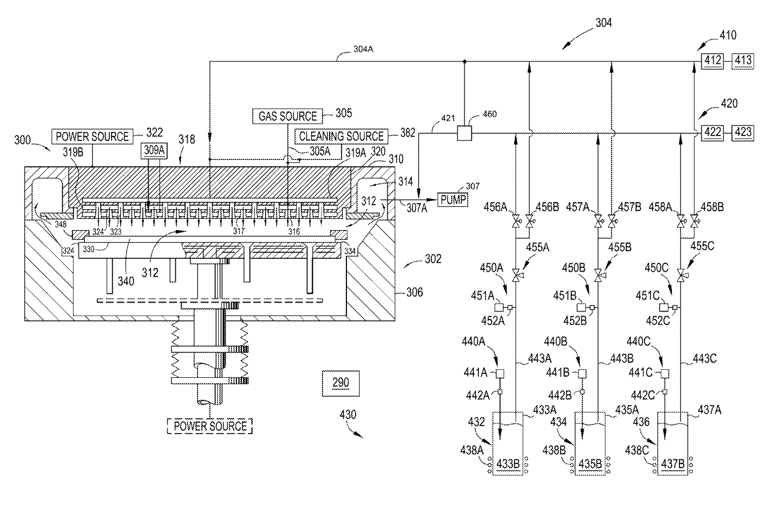
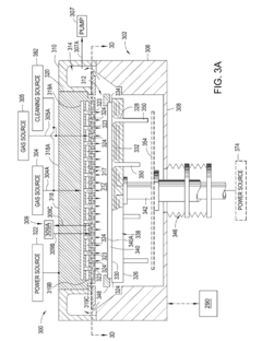
Apparatus and method of forming an indium gallium zinc oxide layer
PatentActiveUS9214340B2
Innovation
- A method and apparatus for forming a multi-element containing film using a gas distribution plate assembly with a precursor plenum and heat exchanging channel, allowing for precise control of precursor gas flow and composition, enabling the deposition of IGZO layers with tailored stoichiometry and reduced environmental exposure.
Environmental Impact of IGZO Manufacturing Processes
The manufacturing processes of IGZO (Indium Gallium Zinc Oxide) thin films present both environmental challenges and opportunities compared to traditional semiconductor materials. The production of IGZO involves several energy-intensive processes including sputtering, chemical vapor deposition, and annealing, which contribute to its environmental footprint. However, IGZO manufacturing typically requires lower processing temperatures (200-300°C) compared to conventional silicon-based semiconductors (>1000°C), resulting in significantly reduced energy consumption during production.
A critical environmental concern is the use of indium, a rare earth metal with limited global reserves. Current estimates suggest that indium supplies may face constraints within the next few decades if consumption continues to increase at present rates. This scarcity has prompted research into indium recycling technologies and alternative material compositions that maintain IGZO's beneficial properties while reducing dependence on scarce elements.
Water usage represents another significant environmental factor in IGZO production. The manufacturing process requires ultra-pure water for cleaning and processing, with estimates indicating that producing one square meter of IGZO film may consume between 1,500-2,000 liters of water. Advanced facilities have implemented closed-loop water recycling systems that can reduce freshwater requirements by up to 60%, substantially mitigating this impact.
Chemical waste management presents ongoing challenges in IGZO manufacturing. The etching processes utilize acids and other potentially hazardous chemicals that require careful handling and disposal. Leading manufacturers have developed specialized treatment systems that neutralize these wastes before discharge, with recovery rates for some chemicals reaching 80-90%, significantly reducing environmental contamination risks.
The environmental advantages of IGZO become more apparent when considering the full lifecycle of devices incorporating this technology. IGZO-based displays consume 50-70% less power than conventional TFT displays, extending battery life and reducing overall energy consumption throughout the product lifecycle. This operational efficiency partially offsets the environmental impacts of manufacturing.
Recent innovations in green manufacturing techniques for IGZO include solvent-free deposition methods, bio-inspired catalysts that reduce chemical usage, and low-temperature processing techniques that further decrease energy requirements. These advancements suggest a promising trajectory toward more sustainable IGZO production methodologies, with several major manufacturers committing to carbon-neutral IGZO manufacturing by 2030 through a combination of process optimization and renewable energy integration.
Supply Chain Considerations for IGZO Materials
The IGZO (Indium Gallium Zinc Oxide) supply chain presents unique challenges and opportunities that significantly impact semiconductor manufacturing efficiency. The primary raw materials—indium, gallium, zinc, and oxygen—each have distinct supply considerations that affect overall production stability. Indium, a critical component, faces supply constraints due to its status as a by-product of zinc mining, with China controlling approximately 57% of global production. This concentration creates potential bottlenecks and price volatility that manufacturers must navigate through strategic sourcing agreements.
Gallium similarly presents supply challenges, with over 95% of global production concentrated in China, Russia, and South Korea. The geopolitical implications of this concentration necessitate diversification strategies for semiconductor manufacturers implementing IGZO technology. Zinc, while more abundant, requires high-purity processing for IGZO applications, adding complexity to material qualification processes.
The manufacturing ecosystem for IGZO materials involves specialized deposition equipment suppliers, primarily dominated by companies in Japan, South Korea, and Taiwan. These suppliers have developed proprietary sputtering and chemical vapor deposition technologies optimized for IGZO thin film production. The technical specifications for IGZO materials require tight tolerances for film uniformity and composition, creating interdependencies between material suppliers and equipment manufacturers that must be carefully managed.
Logistics considerations for IGZO materials include specialized handling requirements due to the sensitivity of precursor materials to environmental conditions. Temperature-controlled transportation and storage facilities are essential throughout the supply chain, adding complexity and cost to material management systems. Additionally, the shelf life limitations of certain IGZO precursors necessitate just-in-time delivery systems that must be balanced against inventory risk management.
Quality control represents another critical dimension of the IGZO supply chain. The performance characteristics of semiconductor devices utilizing IGZO thin films are highly dependent on material purity and consistency. This necessitates sophisticated analytical capabilities throughout the supply chain, from raw material suppliers to final device manufacturers. Traceability systems that can track material properties from source to final application have become increasingly important for yield management and problem resolution.
Sustainability considerations are also reshaping the IGZO supply chain. The rare nature of indium has prompted research into recycling technologies and alternative material formulations. Several leading manufacturers have established closed-loop systems to recover indium and gallium from production waste and end-of-life products, reducing dependency on primary material sources while addressing environmental concerns associated with extraction industries.
Unlock deeper insights with PatSnap Eureka Quick Research — get a full tech report to explore trends and direct your research. Try now!
Generate Your Research Report Instantly with AI Agent
Supercharge your innovation with PatSnap Eureka AI Agent Platform!